Table of Contents
Advertisement
Quick Links
Introduction
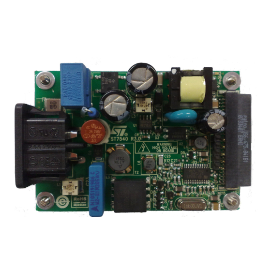
The ST7540 reference design has been developed as a useful tool to demonstrate how a
small, high-performance powerline node can be built using the ST7540 FSK transceiver.
With this reference design, it is possible to evaluate the ST7540 features, in particular, its
transmitting and receiving performances through actual communication on the power line.
The ST7540 reference design may be considered to be composed of three main sections:
●
Power supply section, specifically tailored to match powerline coupling requirements
and to operate within a wide range of the input mains voltage
●
Modem and crystal oscillator section
●
Line coupling interface section
The coupling interface is designed to allow the ST7540 FSK transceiver to transmit and
receive on the mains using 72 kHz carrier frequencies, within the European CENELEC
standard A-band specified for automatic meter reading.
Figure 1.
As it can be seen from the picture above, a special effort has been made to obtain a very
compact reference design board, while keeping the focus on transmission and receiving
performances.
Note:
The information provided in this application note refers to EVALST7540-2 reference design
board.
January 2010
ST7540 reference design board with outline dimensions
Doc ID 12791 Rev 3
Application note
ST7540 FSK powerline transceiver
design guide for AMR
76 mm
AN2451
1/55
www.st.com
Advertisement
Table of Contents

Related Manuals for ST ST7540


Summary of Contents for ST ST7540
-
Page 1: Figure 1. St7540 Reference Design Board With Outline Dimensions
AMR Introduction The ST7540 reference design has been developed as a useful tool to demonstrate how a small, high-performance powerline node can be built using the ST7540 FSK transceiver. With this reference design, it is possible to evaluate the ST7540 features, in particular, its transmitting and receiving performances through actual communication on the power line. -
Page 2: Table Of Contents
Safety precautions ......... . 9 ST7540 FSK powerline transceiver description ....10 Evaluation tools description . - Page 3 AN2451 Contents Appendix A Board layout ..........51 List of normative references .
- Page 4 List of figures Figure 1. ST7540 reference design board with outline dimensions ......1 Figure 2.
- Page 5 AN2451 List of figures Figure 44. Peak detector electrical schematic ......... . . 45 Figure 45.
- Page 6 ST parts on the ST7540 reference design board ....... .
-
Page 7: Electrical Characteristics
AN2451 Electrical characteristics Electrical characteristics Table 1. Electrical characteristics of the ST7540 reference design Value Parameter Test conditions Unit Operating conditions If ST7540 junction temperature Ambient operating temperature exceeds 180 °C device shuts °C down Transceiver section transmitting specifications (Tx mode) -
Page 8: Figure 2. Typical Curve For Output Current Limit Vs. Rcl Value
Electrical characteristics AN2451 Table 1. Electrical characteristics of the ST7540 reference design (continued) Value Parameter Test conditions Unit Number of holdup cycles Input power Switching frequency Transceiver section in Tx mode -10% +10% Transceiver section in Rx Switching frequency -10%... -
Page 9: Safety Precautions
Do not connect any oscilloscope probes to high voltage sections in order to avoid damaging instruments and demonstration tools. Warning: ST assumes no responsibility for any consequences which may result from the improper use of this tool. Doc ID 12791 Rev 3... -
Page 10: St7540 Fsk Powerline Transceiver Description
When in transmission mode (i.e. RxTx line at low level), the ST7540 samples the digital signal on the TxD line at the programmed baud rate and modulates it in a FSK sinusoidal output on the Tx_OUT line. -
Page 11: Evaluation Tools Description
The device also recovers the synchronism of the received signal using an internal PLL. The recovered clock is present on CLR/T output. The ST7540 operating parameters can be set by means of an internal control register, accessible only through the SPI host interface. -
Page 12: Figure 5. St7540 Powerline Modem Demonstration Kit With Control Register Window
Figure 5. ST7540 powerline modem demonstration kit with control register window The complete chain, controlled by the ST7540 powerline modem demonstration kit, can set up real communication at bit level, simply by sending or receiving a user-defined bit stream. It is possible to establish a half-duplex communication with two of these communication nodes (two chains) connected to each other. -
Page 13: Board Description
AN2451 Board description Board description The ST7540 reference design is composed of the following sections: ● Power supply section, based on ST’s VIPer12A-E IC ● ST7540 modem and crystal oscillator section ● Line coupling interface section, with three subsections: –... -
Page 14: Figure 7. Modem And Coupling Interface Schematic
Board description AN2451 Figure 7. Modem and coupling interface schematic HIGH VOLTAGE SECTION 14/55 Doc ID 12791 Rev 3... -
Page 15: Figure 8. Power Supply Schematic
AN2451 Board description Figure 8. Power supply schematic DRAIN HIGH VOLTAGE SECTION Doc ID 12791 Rev 3 15/55... - Page 16 Board description AN2451 Table 3. Bill of materials Item Qty Part Value Description HEADER 2 Mains supply connector CON50A 50 pins SMT right angle female p=1.27mm 33nF X2 Murata GA355XR7-GB333K C2,C3 10uF / 400V Yageo SE-K / Nichicon VK 20% 470pF / 1kV TDK C4520X7R-3A471K 220pF / 50V...
- Page 17 0603 1% 0603 1% 0603 1% 0603 1% SMPS TDK SRW12.6EF-E07H013 / transformer WE S06-100-057 Line VAC T60403-K5024-X044 / transformer Radiohm 69H14-2101 VIPER12AS SMPS controller / switch SFH610-A Opto-switch ST7540 Powerline transceiver 16 MHz Doc ID 12791 Rev 3 17/55...
-
Page 18: Coupling Interface
5.1.1, 5.1.2, and 5.1.3. In each section, calculations and measured frequency responses are given. The filters are quite sensitive to the components' value tolerance. Actual components used in the ST7540 reference design have the following tolerances: ● +/- 10% for coils and for the X2 capacitor ●... -
Page 19: Tx Active Filter
Schematic of Rx and Tx filters 5.1.1 Tx active filter The Tx active filter is based on the ST7540 internal power amplifier (PA), whose input and output pins are available externally to allow a filtering network to be tailored around the amplifier. -
Page 20: Tx Passive Filter
Board description AN2451 Figure 10. Measured frequency response of the Tx active filter (typical curve) Simulation of the Tx active filter response against components' tolerance, depicted in Figure 11, shows +/- 1 dB variation in gain module at 72 kHz. Figure 11. - Page 21 AN2451 Board description provided that the dc-decoupling capacitor C22 is much greater than C23 (in this case, 100 times greater) and that parasitic components of the transformer have negligible effects on the filtering action. Particular attention has been paid in choosing the line transformer. The required characteristics are listed in Table In order to have a good power transfer and to minimize the insertion losses, it is...
-
Page 22: Rx Passive Filter
Board description AN2451 Figure 12. Measured frequency response of the Tx active + passive filters connected to the CISPR network (typical curve) Figure 13. Simulated frequency response of the Tx active + passive filters connected to the CISPR network with the components tolerance effect ... -
Page 23: Figure 14. Measured Frequency Response Of The Rx Passive Filter (Typical Curve)
AN2451 Board description Equation 5 ------ ω • ≅ --------------------------------------- ω • ------ --------------------------- Q ------------------------- - 2π 2π 2π L The simplification made on fc formula is possible because R >R . Consequently, the quality factor and filter selectivity depend not only on R , but also on R . -
Page 24: Input Impedance
In both figures channel impedance point and the minimum impedance point are indicated. The impedance magnitude values prove that the ST7540 reference design board is compliant with the EN50065-7 document, which sets the following minimum impedance constraints for this kind of equipment: ●... -
Page 25: Conducted Disturbances
AN2451 Board description Figure 16. Measured input impedance magnitude of coupling interface in Tx mode (typical curve) Figure 17. Measured input impedance magnitude of coupling interface in Rx mode (typical curve) Conducted disturbances 5.2.1 Conducted emissions The EN50065-1 standard describes the test setup and procedures for testing conducted emissions. -
Page 26: Noise Immunity
Noise immunity The tests on immunity against white noise and narrow-band conducted interferences are based on two ST7540 reference design boards performing a simplex (unidirectional) communication. The first board transmits a given bit sequence, while the receiving board passes the received bit stream to a BER tester software on a PC, which evaluates the percentage of correctly received bits. -
Page 27: Figure 20. Narrow-Band Conducted Interference Test Setup
The received signal and noise levels are measured at the mains connector of the board under test. The 3 kHz resolution bandwidth chosen for the Spectrum Analyzer allows measurement of the actual signal and noise levels as seen by the receiving ST7540 internal circuitry, programmed for 2400 baud. -
Page 28: Figure 21. Measured Ber Vs. Snr Curve (Typical), White Noise
Board description AN2451 Figure 21. Measured BER vs. SNR curve (typical), white noise BER vs. Signal to Noise Ratio 1.00E-01 S/N @ CISPR S/N @ Rx_IN 1.00E-02 1.00E-03 1.00E-04 1.00E-05 1.00E-06 10.0 11.0 12.0 13.0 14.0 15.0 16.0 17.0 18.0 For narrow-band interference tests, two types of interfering noise have been used: a pure sinusoidal tone and an amplitude-modulated signal (modulating signal 1 kHz, modulation depth 80%). -
Page 29: Thermal Design
AN2451 Board description Thermal design All heat dissipation is based on the heat exchange between the ST7540 IC, the PCB and the surrounding environment. A large PCB copper area under the device is recommended to make an easier heat transfer from the ST7540 to the environment. -
Page 30: Figure 24. Packet-Fragmented Transmission
Board description AN2451 Figure 24. Packet-fragmented transmission Transmission Idle in progress state IDLE When soldered to a proper copper area on the PCB as explained above, the IC is characterized by a steady-state thermal impedance of about 35 °C/W. The transient of the thermal impedance θ... -
Page 31: Figure 26. Output Current Vs. Supply Current Typical Curve For St7540 In Tx Mode
AN2451 Board description Figure 26. Output current vs. supply current typical curve for ST7540 in Tx mode The transmission output level V of 2 V and the current limit I of 500 mA, OUT rms OUT rms(LIMIT) fixed for the ST7540 reference design, correspond to a maximum output power P of 1 W over a 4 Ω... -
Page 32: Oscillator Section
Board description AN2451 Oscillator section The ST7540 crystal oscillator circuitry is based on a MOS amplifier working in inverter configuration. This circuitry requires a crystal with a maximum load capacitance of 16 pF and a maximum ESR of 40 Ω. -
Page 33: Figure 29. Common Mode Disturbances Protection - Positive Disturbance
Figure Figure 30 Figure 31 illustrate the protection criteria implemented in the ST7540 reference design. Figure 29 Figure 30 show the protection against common mode disturbances. The BAT54S diodes are intended to prevent the voltage on PA_OUT and Rx_IN lines from going above the supply rail (Vcc for PA_OUT and VDC for Rx_IN) or below ground, with a tolerance equal to the forward voltage of the diodes, that is nearly 0.3 V. -
Page 34: Figure 30. Common Mode Disturbances Protection - Negative Disturbance
Board description AN2451 Figure 30. Common mode disturbances protection - negative disturbance Figure 31. Differential mode disturbances protection 34/55 Doc ID 12791 Rev 3... -
Page 35: 50-Pin Connector For The Evalcommboard
● A VDDF_FORCE signal, which forces the microcontroller to refer digital interface levels to the VDDF (VDD) supply voltage provided by the ST7540 reference design board. This way both the modem and the microcontroller “talk” on the same digital levels. -
Page 36: Power Supply
22,34 Ground Power supply The ST7540 reference design includes a specifically designed Switching Mode Power Supply (SMPS) circuit, based on the ST VIPer12AS-E device. The VIPer12AS-E is a smart power device with a current mode PWM controller, a startup circuit and protections integrated in a monolithic chip using VIPower M0 technology. It includes a 27 Ω... - Page 37 AN2451 Board description Table 10. SMPS specifications Parameter Value Input voltage range, V 85-265 Output voltage, V 12 V±10% Peak output current, I 500 mA OUT(MAX) In the input stage, an EMI filter is implemented (C plus C ) for both differential and common mode noise, in order to fit the requested standard.
-
Page 38: Figure 33. Typical Waveforms At 230 Vac: Open Load
Board description AN2451 In any SMPS, protection against an output short-circuit is very important. All tests have been done by shorting the SMPS output at maximum input voltage. The results are given in Figure The main parameters are the drain-source voltage (V ), the output current (I ) and the supply voltage (V... -
Page 39: Figure 35. Typical Waveforms At 265 Vac: Short-Circuit
AN2451 Board description Figure 35. Typical waveforms at 265 V Figure 36. Typical waveforms at 265 V short-circuit startup Ch1 freq - 23.50 Hz (green) Ch1 max - 702 V (black) Ch4 max - 2.08 A (light blue) Ch2 mean - 19.72 V (green) Ch4 mean - 383 mA (light blue) Ch4 max - 500 mA (light blue) Figure 37. -
Page 40: Figure 38. Smps Efficiency Curve
Board description AN2451 Figure 38 shows the efficiency vs. output current curve. Minimum efficiency occurs at low- load condition, as expected from any SMPS. This is not an issue for our application, since low efficiency corresponds also to low power consumption and thus to low dissipation. On the other hand, at output current values over 500 mA (full-load condition), both the transformer and the VIPer are forced to operate close to their current limitations and thus the efficiency is reduced. -
Page 41: Performance And Ping Tests
“none”, “BU” or “PD”. In the last two cases, messages are sent to the slave only if the BU or CD/PD lines of the ST7540 modem are not active. If the PD setting is selected, the content of the ST7540 internal control register is changed to select “Preamble”... -
Page 42: Application Ideas
Figure 40 can be used. In that topology, the total impedance that the ST7540 power amplifier is required to drive is equal to the parallel of the impedance seen on each of the three phases, so probably the device will be required to force an higher output current. -
Page 43: Figure 41. Schematic Of A Zero Crossing Detection Circuit For Non-Isolated Coupling
The circuit in Figure 41 is only applicable to a non-isolated board topology. It is not possible to implement it directly on the ST7540 reference design. Figure 41. Schematic of a zero crossing detection circuit for non-isolated coupling BS170F/SOT ZC_OUT... -
Page 44: Received Signal Strength Indicator (Rssi)
Application ideas AN2451 Figure 42. Schematic of a zero crossing detection circuit for isolated coupling If<1m A 25k 1/2W 25k 1/2W ISO1 OPTOCOUPLER 1N4148 ZC_OUT 100k Figure 43. ZC_OUT vs. AC mains waveforms AC Mains ZC_out ZC OUT Received signal strength indicator (RSSI) In many application fields, measuring the strength of the incoming signal is useful to: ●... -
Page 45: Non-Isolated Coupling
AN2451 Application ideas Figure 44. Peak detector electrical schematic 4.7k Rx_IN DC_OUT LM393 1N4148 100n 100k The schematic above is based on a simple diode-capacitor (D1-C1) circuit improved with an LM393 comparator so that: ● The comparator eliminates the diode reverse voltage. ●... -
Page 46: Dc Powerline Applications
D 1 0 BA T54S /SOT DC powerline applications The ST7540 reference design can be adapted to communicate over a DC power line. In this case, the schematic of Figure 46 has to be referred to as line coupling, with two modifications: L7 can be removed and the C23 capacitor can be substituted with a lower voltage ceramic component. -
Page 47: Figure 47. Line Coupling Interface For 110 Khz Channel
AN2451 Application ideas Figure 47. Line coupling interface for 110 kHz channel Doc ID 12791 Rev 3 47/55... -
Page 48: Figure 48. Line Coupling Interface For 132.5 Khz Channel
Application ideas AN2451 Figure 48. Line coupling interface for 132.5 kHz channel 48/55 Doc ID 12791 Rev 3... -
Page 49: Troubleshooting
If the current-limit mode is forced on the transceiver, modify the value of the R6 feedback resistor to exit from limitation according to the actual load forced by the mains network. Problem: the ST7540 reference design board transmits only for a short time. What to check: Check the transmission timeout setting. - Page 50 Check the preamble detection setting on the control register panel of the ST7540 powerline modem demonstration kit window. Check if data are present on the RxD pin. Problem: during a ping test or a transmission test, the ST7540 reference design board shows high bit error rate. Note: This point refers to a half-duplex communication involving two ST7540 reference design boards communicating with each other.
-
Page 51: Figure 49. Pcb Layout - Component Placing
AN2451 Board layout Appendix A Board layout Figure 49. PCB layout - component placing Doc ID 12791 Rev 3 51/55... -
Page 52: Figure 50. Pcb Layout - Top View
Board layout AN2451 Figure 50. PCB layout - top view 52/55 Doc ID 12791 Rev 3... -
Page 53: Figure 51. Pcb Layout - Bottom View
AN2451 Board layout Figure 51. PCB layout - bottom view Doc ID 12791 Rev 3 53/55... -
Page 54: List Of Normative References
List of normative references AN2451 List of normative references EN50065: Signaling on low voltage electrical installations in the frequency range 3 kHz to 148.5 kHz. ● Part 1: General requirements, frequency bands and electromagnetic disturbances ● Part 2-1: Immunity requirements ●... - Page 55 No license, express or implied, by estoppel or otherwise, to any intellectual property rights is granted under this document. If any part of this document refers to any third party products or services it shall not be deemed a license grant by ST for the use of such third party products or services, or any intellectual property contained therein or considered as a warranty covering the use in any manner whatsoever of such third party products or services or any intellectual property contained therein.
Need help?
Do you have a question about the ST7540 and is the answer not in the manual?
Questions and answers