Sign In
Upload
Manuals
Brands
ST Manuals
Transceiver
ST7540
User Manuals: ST ST7540 Power Line Transceiver
Manuals and User Guides for ST ST7540 Power Line Transceiver. We have
1
ST ST7540 Power Line Transceiver manual available for free PDF download: Application Note
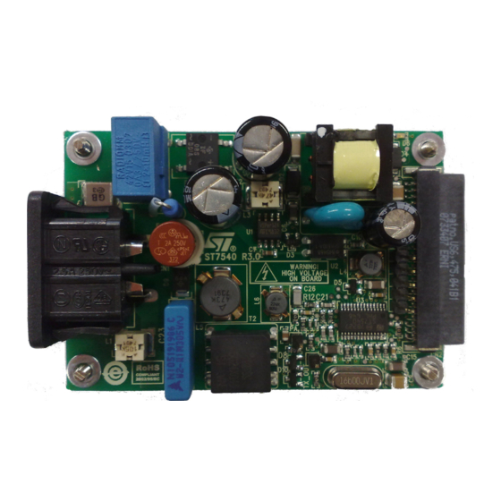
ST ST7540 Application Note (55 pages)
FSK powerline transceiver design guide for AMR
Brand:
ST
| Category:
Transceiver
| Size: 2 MB
Table of Contents
Figure 1. ST7540 Reference Design Board with Outline Dimensions
1
Table of Contents
2
1 Electrical Characteristics
7
Figure 2. Typical Curve for Output Current Limit Vs. RCL Value
8
2 Safety Precautions
9
3 ST7540 FSK Powerline Transceiver Description
10
Figure 3. ST7540 Transceiver Block Diagram
10
4 Evaluation Tools Description
11
Figure 4. Complete Evaluation System Including a PC, an EVALCOMMBOARD and the EVALST7540-2 Board
11
Figure 5. ST7540 Powerline Modem Demonstration Kit with Control Register Window
12
5 Board Description
13
Figure 6. Positioning of the Various Sections of the Board
13
Figure 7. Modem and Coupling Interface Schematic
14
Figure 8. Power Supply Schematic
15
Coupling Interface
18
Tx Active Filter
19
Figure 9. Schematic of Rx and Tx Filters
19
Tx Passive Filter
20
Figure 10. Measured Frequency Response of the Tx Active Filter (Typical Curve)
20
Figure 11. Simulated Frequency Response of the Tx Active Filter with Components Tolerance Effect
20
Rx Passive Filter
22
Figure 12. Measured Frequency Response of the Tx Active + Passive Filters Connected to the CISPR Net
22
Figure 14. Measured Frequency Response of the Rx Passive Filter (Typical Curve)
23
Input Impedance
24
Figure 15. Simulated Frequency Response of the Rx Passive Filter with Components Tolerance Effect
24
Conducted Disturbances
25
Conducted Emissions
25
Figure 16. Measured Input Impedance Magnitude of Coupling Interface in Tx Mode (Typical Curve)
25
Figure 17. Measured Input Impedance Magnitude of Coupling Interface in Rx Mode (Typical Curve)
25
Noise Immunity
26
Figure 18. Conducted Emissions Test Setup
26
Figure 19. Output Spectrum (Typical) at 72 Khz, 2400 Baud, Deviation 1, Mains 220Vac
26
Figure 20. Narrow-Band Conducted Interference Test Setup
27
Figure 21. Measured BER Vs. SNR Curve (Typical), White Noise
28
Figure 22. SNR Vs. Frequency Curve (Typical) at BER = 10-3
28
Figure 23. PCB Copper Dissipating Area for ST7540 Reference Design Board
29
Thermal Design
29
Figure 24. Packet-Fragmented Transmission
30
Figure 25. Equivalent Model of the Thermal Impedance Qja of the HTSSOP28 Package with Exposed Pad
30
Figure 26. Output Current Vs. Supply Current Typical Curve for ST7540 in Tx Mode
31
Figure 27. Dissipated Power Vs. Load Impedance Modulus Typical Curve for ST7540 Reference Design Board
31
Figure 28. a Recommended Oscillator Section Layout for Noise Shielding
32
Oscillator Section
32
Surge and Burst Protection
32
Figure 29. Common Mode Disturbances Protection - Positive Disturbance
33
Figure 30. Common Mode Disturbances Protection - Negative Disturbance
34
Figure 31. Differential Mode Disturbances Protection
34
50-Pin Connector for the EVALCOMMBOARD
35
Figure 32. Scheme of the Connector for the EVALCOMMBOARD
35
Power Supply
36
Figure 33. Typical Waveforms at 230 Vac: Open Load
38
Figure 34. Typical Waveforms at 230 Vac: Full Load
38
Figure 35. Typical Waveforms at 265 Vac: Short-Circuit
39
Figure 36. Typical Waveforms at 265 Vac: Startup
39
Figure 37. Load Regulation
39
Figure 38. SMPS Efficiency Curve
40
6 Performance and Ping Tests
41
Figure 39. ST7540 Powerline Modem Demonstration Kit Window for the Master Board
41
7 Application Ideas
42
Three-Phase Architecture
42
Zero Crossing Detector
42
Figure 40. Scheme of Principle for Three-Phase Architecture
42
Figure 41. Schematic of a Zero Crossing Detection Circuit for Non-Isolated Coupling
43
Received Signal Strength Indicator (RSSI)
44
Figure 42. Schematic of a Zero Crossing Detection Circuit for Isolated Coupling
44
Figure 43. ZC_OUT Vs. AC Mains Waveforms
44
Non-Isolated Coupling
45
Figure 44. Peak Detector Electrical Schematic
45
Figure 45. Measured DC_OUT Vs. AC_IN Peak Detector Response
45
DC Powerline Applications
46
110 And 132.5 Khz Coupling Circuit
46
Figure 46. Example Schematic for Non-Isolated Solution
46
Figure 47. Line Coupling Interface for 110 Khz Channel
47
Figure 48. Line Coupling Interface for 132.5 Khz Channel
48
8 Troubleshooting
49
Figure 49. PCB Layout - Component Placing
51
Appendix A Board Layout
51
Figure 50. PCB Layout - Top View
52
Figure 51. PCB Layout - Bottom View
53
List of Normative References
54
Advertisement
Advertisement
Related Products
ST ST7538Q
ST ST802RT1A
ST ST802RT1B
ST Sigfox S2-LP
ST ST75 Series
ST ST7570
ST ST7580
ST ST7590
ST ST7232A
ST ST72F32AJ1
ST Categories
Motherboard
Computer Hardware
Microcontrollers
Control Unit
Controller
More ST Manuals
Login
Sign In
OR
Sign in with Facebook
Sign in with Google
Upload manual
Upload from disk
Upload from URL