Table of Contents
Advertisement
Quick Links
Introduction
The ST7538Q dual channel reference design is a practical tool to start the activity of
designing an automatic meter reading (AMR) node based on the ST7538Q power line FSK
transceiver.
With this reference design, it is possible to evaluate the features of the ST7538Q and its
transmitting and receiving performances in an actual communication on the power line
network.
The ST7538Q reference design can be considered as composed of three main sections:
■
power supply section, specifically designed to coexist with power line communication and
to operate from a wide-range input mains voltage
■
modem and crystal oscillator section
■
dual channel line coupling interface section
The dual channel line coupling interface allows the ST7538Q FSK transceiver to transmit
and receive on the mains using two different carrier frequencies: 72 kHz and 86 kHz, both
within the frequency band A specified by the European CENELEC EN50065 standard for
AMR applications.
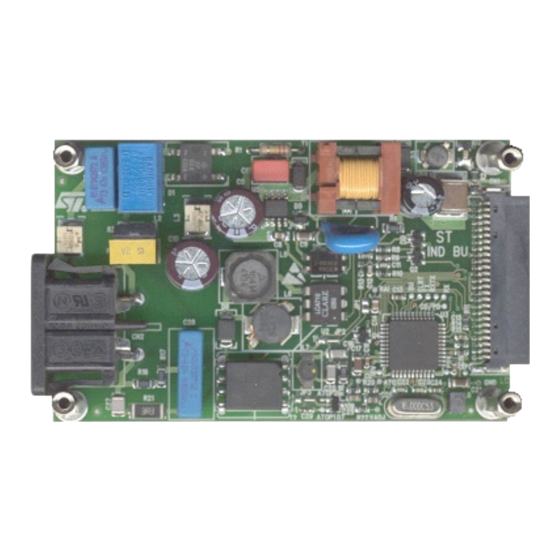
Figure 1.
As it can be seen from the picture above, a special effort has been made to develop a
compact reference design board, oriented to practical applications.
Note:
The information provided in this application note refers to the EVALST7538DUAL reference
design board.
April 2008
ST7538Q power line FSK transceiver
dual channel reference design for AMR
ST7538Q dual channel reference design board with outline dimensions
Application note
98mm
Rev 1
AN2744
1/56
www.st.com
56
Advertisement
Table of Contents

Subscribe to Our Youtube Channel
Related Manuals for ST ST7538Q


Summary of Contents for ST ST7538Q
-
Page 1: Figure 1. St7538Q Dual Channel Reference Design Board With Outline Dimensions
(AMR) node based on the ST7538Q power line FSK transceiver. With this reference design, it is possible to evaluate the features of the ST7538Q and its transmitting and receiving performances in an actual communication on the power line network. -
Page 2: Table Of Contents
Safety precautions ......... . 9 ST7538Q FSK power line transceiver description ....10 Evaluation tools description . - Page 3 AN2744 Contents Appendix A Board layout ..........53 Revision history .
- Page 4 ST7538Q transceiver block diagram ........
- Page 5 AN2744 List of figures Figure 37. Common mode disturbances protection ........39 Figure 38.
- Page 6 Bill of materials ............17 Table 4. ST parts on the ST7538Q dual channel reference design board ....19 Table 5.
-
Page 7: Electrical Characteristics
AN2744 Electrical characteristics Electrical characteristics Table 1. Electrical characteristics of the ST7538Q dual channel reference design Parameter Value Notes Min. Typ. Max. Operating condition If junction temperature Ambient operating 85 °C exceeds 180 °C the device temperature shuts down Transceiver section... -
Page 8: Figure 2. Typical Curve For Output Current Limit Vs. Rcl Value
-10% 60 kHz +10% Transceiver section in Tx mode 1. ST does not guarantee transformer isolation. ST assumes no responsibility for the consequences that may result from that risk. Table 2. Output signal level setting through V partitioning - typical values... -
Page 9: Safety Precautions
Do not connect any oscilloscope probes to high voltage sections in order to avoid damaging instruments and demonstration tools. Warning: ST assumes no responsibility for any consequences which may result from the improper use of this tool. 9/56... -
Page 10: St7538Q Fsk Power Line Transceiver Description
(CLR/T) provided by the transceiver at the programmed baud rate. When in transmission mode (i.e. RxTx line at low level), the ST7538Q transceiver samples the data on the TxD line, generating an FSK modulated signal on the ATO pin. The same... - Page 11 When in reception mode (i.e. RxTx line at high level), an incoming signal at the RAI line is demodulated and converted to a digital bit stream on the RxD pin. The internal control register, which contains the operating parameters of the ST7538Q transceiver, can be programmed only using the SPI interface. The control register settings include the header recognition and frame length count functions, which can be used to apply byte and frame synchronization to the received messages.
-
Page 12: Evaluation Tools Description
Evaluation tools description AN2744 Evaluation tools description The complete evaluation environment for the ST7538Q power line communication consists – 1 PC using the "ST7538 power line modem demonstration kit" software tool – 1 EVALCOMMBOARD hosting an ST7 microcontroller – 1 ST7538Q dual channel reference design board (EVALST7538DUAL) -
Page 13: Figure 5. Power Line Modem Demonstration Kit With Transmission Session Window
This feature can be enabled in the Rx panel of the ST7538Q power line modem demonstration kit. A bit synchronization can be introduced as a simpler feature by enabling the preamble detection method in the control register panel and then inserting at least one "0101"... -
Page 14: Board Description
Board description AN2744 Board description The ST7538Q dual channel reference design is composed of the following sections: – power supply section, based on ST’s VIPer12A-E IC – ST7538Q modem and crystal oscillator section – line coupling interface section, with three subsections: –... -
Page 15: Figure 7. Modem And Coupling Interface Schematic
AN2744 Board description Figure 7. Modem and coupling interface schematic 15/56... -
Page 16: Figure 8. Power Supply Schematic
Board description AN2744 Figure 8. Power supply schematic 16/56... -
Page 17: Table 3. Bill Of Materials
AN2744 Board description Table 3. Bill of materials Item Q.ty Reference Value Description ATOP1, ATOP2, P5 V, 10 V, VADJ, TX, RXTX, RXFO, RX, Test point RAI, GND, CLRT, CL, CD/PD, BU, ATO CON50A 50-pin female connector Header 2 Mains supply connector 470 pF 630 V EVOX-RIFA PFR5-471J630L4 47 nF X2... - Page 18 2 kΩ 10 kΩ SMPS transformer TDK SRW12.6ES-ExxH013 / Würth S06-100-057 Line transformer VAC T60403-K5024-X044 / Radiohm 69H14-2101 SFH610-A Optoswitch LCA710 Optoswitch - 3750 V isolation ST7538Q Power line transceiver VIPer12AS-E SMPS controller / switch 16 Mhz Jauch Q 16.0-SS2-16-30/50-FU 18/56...
-
Page 19: Table 4. St Parts On The St7538Q Dual Channel Reference Design Board
AN2744 Board description Table 4. ST parts on the ST7538Q dual channel reference design board Value Description ST7538Q Power line transceiver VIPer12AS-E SMPS controller / switch STTH1L06A Ultrafast diode STPS1H100 Schottky diode SM6T6V8CA 6.8 V bidirectional Transil™ diode ESDA6V1L 6.1 V ESD Transil™ diode... -
Page 20: Line Coupling Interface
The filters are quite sensitive to the components' value tolerance. Actual components used in the ST7538Q dual channel reference design have the following tolerances: ● +/- 10% for coils and for the X2 capacitor ●... -
Page 21: Dual Channel Selection
Dual channel selection To obtain a dual channel interface, each filter is tunable via software command. The ST7538Q dual channel reference design has two available channel frequencies, 72 and 86 kHz. The channel can be simply changed by including or excluding one passive component per each filter: an inductor for the Tx filter, a capacitor for the Rx passive filter and a resistor for the Rx active filter. -
Page 22: Figure 10. Measured Frequency Response Of The Tx Passive Filter For 72 Khz Channel (Typical)
Board description AN2744 Table 5. Line coupling transformer specifications Parameter Value Turn Ratio Magnetizing Inductance > 1 mH Leakage Inductance < 1 µH < 0.5 Ω DC total resistance DC saturation current > 2 mA Interwinding capacitance < 50 pF Withstanding Voltage 4 kV Figure 10... -
Page 23: Figure 11. Measured Frequency Response Of The Tx Passive Filter For 86 Khz Channel (Typical)
AN2744 Board description Figure 11. Measured frequency response of the Tx passive filter for 86 kHz channel (typical) CISPR CISPR 5 Ω load 5 Ω load 1E+04 1E+04 1E+05 1E+05 1E+06 1E+06 Freq (Hz) Freq (Hz) Simulations of the filter for both frequency channels, given in Figure 12 Figure 13 , show... -
Page 24: Dual Channel Rx Passive Filter
Board description AN2744 Figure 13. Simulated frequency response of the Tx passive filter for 86 kHz channel with tolerance effect 5.1.3 Dual channel Rx passive filter The dual channel Rx passive filter is made of a resistor in series with a parallel L-C resonant circuit. -
Page 25: Figure 14. Measured Frequency Response Of The Rx Passive Filter For 72 Khz Channel (Typical)
AN2744 Board description higher selectivity. The values of the actual components give a Q of about 2.2 for the 72 kHz channel and 1.8 for the 86 kHz channel. The value of R impacts more obviously on insertion losses. To evaluate the relationship between R and the losses on received signal, the following simplified expression of |R | at... -
Page 26: Figure 15. Measured Frequency Response Of The Rx Passive Filter For 86 Khz Channel (Typical)
Board description AN2744 Figure 15. Measured frequency response of the Rx passive filter for 86 kHz channel (typical) 1E+04 1E+04 1E+05 1E+05 1E+06 1E+06 Freq (Hz) Freq (Hz) It can be observed from the simulation curves of Figure 16 Figure 17 a maximum loss at center frequency of 1 dB due to the spread of the components' value. -
Page 27: Dual Channel Rx Active Filter
An active filtering is suitable for receiving a highly attenuated signal. Without the gain of an active filter, it could be impossible to detect a signal lower than the ST7538Q receiving sensitivity even filtering the noise around it. Therefore, the choice of the Rx filter depends mostly on the attenuation introduced by the network and then on the point of insertion of the power line communication node. -
Page 28: Figure 19. Measured Frequency Response Of The Rx Active Filter For 86 Khz Channel (Typical)
Board description AN2744 Figure 19. Measured frequency response of the Rx active filter for 86 kHz channel (typical) 1.0E+04 1.0E+04 1.0E+05 1.0E+05 1.0E+06 1.0E+06 Freq (Hz) Freq (Hz) Figure 20 Figure 21 show the simulation results with Montecarlo analysis. The gain variation at center frequency is less than 2 dB. -
Page 29: Input Impedance
Tx and Rx mode for the two channels. The impedance magnitude values prove that the ST7538Q dual channel reference design board is compliant with EN50065-7 normative, which sets the following minimum impedance constraints for this kind of equipment: –... -
Page 30: Figure 23. Measured Input Impedance Magnitude Of The Coupling Interface In Rx Mode For The 86 Khz Channel (Typical Curve)
Board description AN2744 Figure 23. Measured input impedance magnitude of the coupling interface in Rx mode for the 86 kHz channel (typical curve) 1000 1000 EN50065 EN50065- EN50065 EN50065- 1E+04 1E+04 1E+05 1E+05 1E+06 1E+06 Freq (Hz) Freq (Hz) Figure 24. Measured input impedance magnitude of the coupling interface in Tx mode for the 72 kHz channel (typical curve) 1000 1000... -
Page 31: Conducted Disturbances
AN2744 Board description Figure 25. Measured input impedance magnitude of the coupling interface in Tx mode for the 86 kHz channel (typical curve) 1000 1000 EN50065 EN50065- EN50065 EN50065- 1E+04 1E+04 1E+05 1E+05 1E+06 1E+06 Freq (Hz) Freq (Hz) Conducted disturbances 5.2.1 Conducted emissions The EN50065-1 standard describes test setup and procedures for this kind of test. -
Page 32: Figure 26. Conducted Disturbance Test Setup
EN50065-1 disturbance limits mask is traced in red. It may be compared with the typical output spectrum of the ST7538Q dual channel reference design board for each channel. Figure 27. Output spectrum (typical) at 72 kHz channel, mains 220 V , fixed transmitted tone = "1"... -
Page 33: Noise Immunity
AN2744 Board description Figure 28. Output spectrum (typical) at 86 kHz channel, mains 220 V , fixed transmitted tone = "1" 130.0 130.0 =84.8 kHz =84.8 kHz S=120.1 dBµV S=120.1 dBµV 120.0 120.0 110.0 110.0 100.0 100.0 =169.6 kHz =169.6 kHz 90.0 90.0 S=58.6 dBµV... -
Page 34: Figure 30. Measured Ber Vs. Snr Curve (Typical), White Noise
The received signal and noise level are measured with a spectrum analyzer at both the ST7538Q RAI pin and the measurement port of the CISPR artificial network. To obtain the right value, the noise level is measured in absence of the transmitted signal. The 3 kHz resolution bandwidth of the spectrum analyzer has been chosen to fit the spectrum of the transmitted FSK signal at 2400 baud. -
Page 35: Figure 31. Measured Snr Vs. Frequency Curves (Typical) At Ber=10-3 - 72 Khz Channel
AN2744 Board description For narrowband interference tests, two types of interfering noise have been used: a pure sinusoidal tone and an amplitude-modulated signal, (modulating signal 1 kHz, modulation depth 80%). In these tests, the amplitude of the noise tone (or the carrier, in case of modulated interferer) is varied until the measured BER reaches 10 (one error every 1000 transmitted bits). -
Page 36: Thermal Design
Board description AN2744 Thermal design All heat dissipation is based on the heat exchange between the ST7538Q IC, the PCB and the environment. A large PCB copper area under the device is recommended in order to achieve a better heat... -
Page 37: Figure 34. Packet-Fragmented Transmission
100%. Figure 35. Thermal impedance typical curve for the ST7538Q mounted on the reference design board d=0.75... -
Page 38: Oscillator Section
125 °C limit. Oscillator section The ST7538Q crystal oscillator circuitry is based on a MOS amplifier working in inverter configuration. This circuitry requires a crystal having a maximum load capacitance of 16 pF and a maximum ESR of 40 Ω. -
Page 39: Surge And Burst Protection
1.2 x 50 µs. Fast transient burst tests are specified at level +/- 2 kV, with pulse shape 5 x 50 ns and pulse frequency 5 kHz. Figure 37 Figure 38 illustrate the protection criteria implemented in the ST7538Q reference design. Figure 37 shows the protection against common mode disturbances. The ESD Transil™... -
Page 40: 50-Pin Connector For Communication Board
Table 7 Table 8 Table 9 Beside the ST7538Q input and output signals, the link to the IBU communication board includes: – A 2-bit (B_ID_PLM_1 and B_ID_PLM_0) Board Identification Code, which identifies the hosted power line transceiver. The "00" HW binary configuration makes the microcontroller able to recognize the ST7538Q reference design board. -
Page 41: Figure 39. Scheme Of The Communication Board Connector
TOUT CON50A Table 7. 50-pin connector digital signals Pin n° Signal name Description Generated by MCLK Oscillator output (programmable) ST7538Q RESET Reset Out for microcontroller ST7538Q REGOK Register OK signal ST7538Q NEG_CH2 Secondary channel select (active low) µC Secondary channel select (active high) µC... -
Page 42: Power Supply
22,34 Ground Power supply The ST7538Q dual channel reference design includes a specifically designed switching mode power supply circuit, based on ST’s VIPer12AS-E device. VIPer12AS-E is a smart power device with current mode PWM controller, startup circuit and protections integrated in a monolithic chip using VIPower M0 technology. It includes a 27 Ω... -
Page 43: Table 11. Smps Transformer Specifications
AN2744 Board description The blocking diode D4 and the clamping network (R1-C1) clamp the peak of the leakage inductance voltage spike, assuring reliable operation of the VIPer12AS-E. D4 must be not only very fast-recovery but also very fast turn-on type to avoid additional drain overvoltage. The clamp capacitor C1 must be low-loss type (with polypropylene or polystyrene film dielectric) to reduce power dissipation and prevent overheating, since it is charged with high peak currents by the energy stored in the leakage inductance. -
Page 44: Figure 40. Typical Waveforms At 230 Vac: Open Load
Board description AN2744 The startup phase could also be critical for the SMPS as output overshoot occurs if the circuit is not properly designed. Care must be taken in designing a proper clamp network in order to prevent voltage spikes due to leakage inductance from exceeding the breakdown voltage of the device (730 V minimum value). -
Page 45: Figure 44. Load Regulation
AN2744 Board description Figure 44. Load regulation 10.5 10.5 10.4 10.4 10.3 10.3 185 V ac 185 V ac 10.2 10.2 230 V ac 230 V ac 10.1 10.1 265 V ac 265 V ac [mA] [mA] shows the efficiency vs. output current curve. Minimum efficiency occurs at low Figure 44 load condition, as expected from any SMPS. -
Page 46: Performance And Ping Tests
"none", "BU" or "PD". In the last two cases, messages are sent to slave only if BU or CD/PD lines of the ST7538Q modem are not active. If PD setting is selected, content of the ST7538Q internal control register is changed to select "Preamble" as the detection method. -
Page 47: Application Ideas
Application ideas Application ideas Three-phase architecture The ST7538Q modem can be used to communicate on a three-phase network. A microcontroller should switch communication between the three phases, since the modem can transmit/receive over only one phase at a time. In the example scheme of... -
Page 48: Figure 48. Peak Detector Electrical Schematic
Application ideas AN2744 Figure 48. Peak detector electrical schematic 4.7k 4.7k Rx_IN Rx_IN DC_OUT DC_OUT LM393 LM393 1N4148 1N4148 100n 100n 100k 100k The schematic above is based on a simple diode-capacitor (D1-C1) circuit improved with an LM393 comparator so that: ●... -
Page 49: 110-132.5 Khz Dual Channel Coupling Circuit
In this paragraph the dual channel application circuit for CENELEC band B and C is suggested. The 110 and 132.5 kHz channel frequencies of the ST7538Q transceiver are suitable for home automation applications and in general for applications not subject to the European AMR regulations. -
Page 50: Troubleshooting
Check that the AC mains supply cable is well connected to CN2. Check if the green LED D2 is on. Check voltage on the 10 V test point near the ST7538Q. The value must be 9 to 11 PROBLEM : the ST7538Q reference design board is not responding. - Page 51 Check preamble detection setting on the control register panel of the reference design software window. Check if data are present on RxD pin. PROBLEM : During a ping test or a transmission test, the ST7538Q reference design board shows a high bit error rate. Note: This point refers to a half-duplex communication involving two ST7538Q reference design boards communicating with each other.
-
Page 52: List Of Normative References
List of normative references AN2744 List of normative references EN50065 : Signaling on low voltage electrical installations in the frequency range 3 kHz to 148.5 kHz – Part 1: General requirements, frequency bands and electromagnetic disturbances – Part 2-1: Immunity requirements –... -
Page 53: Figure 50. Pcb Layout - Top View
AN2744 Board layout Appendix A Board layout Figure 50. PCB layout - top view 53/56... -
Page 54: Figure 51. Pcb Layout - Bottom View
Board layout AN2744 Figure 51. PCB layout - bottom view 54/56... -
Page 55: Table 13. Document Revision History
AN2744 Revision history Revision history Table 13. Document revision history Date Revision Changes 30-Apr-2008 Initial release. 55/56... - Page 56 No license, express or implied, by estoppel or otherwise, to any intellectual property rights is granted under this document. If any part of this document refers to any third party products or services it shall not be deemed a license grant by ST for the use of such third party products or services, or any intellectual property contained therein or considered as a warranty covering the use in any manner whatsoever of such third party products or services or any intellectual property contained therein.
Need help?
Do you have a question about the ST7538Q and is the answer not in the manual?
Questions and answers