Table of Contents
Advertisement
Quick Links
Advertisement
Table of Contents

Related Manuals for Contec CNT24-4D(PCI)


Summary of Contents for Contec CNT24-4D(PCI)
- Page 1 CNT24-4D(PCI) 24Bit Differencial Up/Down Counter Board for PCI User’s Guide...
-
Page 2: Trademarks
Copyright 2000 CONTEC Co., LTD. ALL RIGHTS RESERVED No part of this document may be copied or reproduced in any form by any means without prior written consent of CONTEC Co., LTD. CONTEC Co., LTD. makes no commitment to update or keep current the information contained in this document. -
Page 3: Product Configuration
Check the contents to make sure that you have everything listed above. If you do not have all the items, contact your distributor or CONTEC group office where you purchased. Note! Do not remove the board from its protective packaging until the computer case is open and ready for installation. -
Page 4: Table Of Contents
Setting One-shot Pulse Output Signals......7 Setting Terminators ............8 3. Board Setup ............. 9 Use CONTEC Windows Software Products.....9 When Not Using CONTEC Software for Windows ..10 For Windows 98 Systems..........10 For Windows 95 Systems..........14 For other OS systems ..........19 4. Connection with External Devices ......21 Interface Connector............21... - Page 5 TTL-level Input Circuit and an Example Connection ........25 Output Circuit and an Example Connection.....25 Example Connection with a Rotary Encoder....27 Measures against Voltage Surges ........28 5. I/O Port Bit Assignment .......... 29 I/O Port Bit Assignment ..........29 Setting Data ..............30 Count Flow ..............31 Operation Commands .............32 Description of Output Commands........34...
- Page 6 Sense Port (Command 16H) ........51 General-purse Input Signal Select (Command 1AH) ............52 Initialization..............53 6. Board Specifications..........55 Block Diagram..............55 Specifications..............56 7. Index ..............59 CNT24-4D(PCI)
- Page 7 List of Figures Figure 2.1. Component Locations..........5 Figure 2.2. Board ID Settings (SW1).......... 6 Figure 2.3. Switch for setting one-shot-pulse output signals ..7 Figure 2.4. Terminator setting switches ........8 Figure 4.1. Connecting the interface connector ......21 Figure 4.2.
- Page 8 Figure 5.7. Example counting during synchronous clear ..37 Figure 5.8. Example counting during asynchronous clear..38 Figure 5.9. Example counting when count input multiplication is set ............... 39 Figure 5.10. Phase Z enable frequency ZSEL=0 (Positive logic) ............40 Figure 5.11.
- Page 9 List of Tables Table 2.1. One-shot-pulse output signal settings......7 Table 2.2. Terminator settings............8 Table 5.1. Output commands ............. 32 Table 5.2. Input commands............33 Table 5.3. Counter operation modes .......... 35 Table 5.4. Switching counting directions ........35 Table 5.5.
-
Page 10: Introduction
Please follow the setup instructions of the User’s manual shipped with the software products and/or the help files of the package to setup our interface board(s) to your system. For details of CONTEC software products, please contact our sales agencies. Features... -
Page 11: Limited Three-Year Warranty
Please obtain a Return Merchandise Authorization Number (RMA) from the CONTEC group office where you purchased before returning any product. * No product will be accepted by CONTEC group without the RMA number. Liability The obligation of the warrantor is solely to repair or replace the product. -
Page 12: Handling Precautions
Introduction Handling Precautions Take the following precautions when handling this board. - Never modify the board. The manufacturer cannot be responsible for any board that has been modified by the user. - Protect the board against shock and do not bend the board or it will be damaged. -
Page 13: About The Manual
Introduction About the Manual This manual consists of the following chapters: Chapter 1 Component Identification and Settings Identifies each component of the board and explains how to set the switch, for example. Chapter 2 Setup Explains how to set up the board to use it. Chapter 3 Board Setup Explains how to set up the board. -
Page 14: Component Locations And Setting
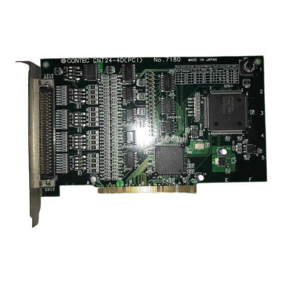
Component Locations and Setting 2. Component Locations and Setting Component Locations Figure 2.1 shows the names of major parts on the board. Note that the switch setting shown below is the factory default. Figure 2.1. Component Locations CNT24-4D(PCI) -
Page 15: Setting The Board Id
Component Locations and Setting Setting the Board ID When installing multiple CNT24-4D (PCI) boards in one PC, you need to set their IDs in order to distinguish one board from another. Each ID should be set to a unique value. A board ID can be set in a range of 0 through F and 16 boards can be distinguished at maximum. -
Page 16: Setting One-Shot Pulse Output Signals
Component Locations and Setting Setting One-shot Pulse Output Signals Set the type of one-shot-pulse output signals with SW2. The TTL-level output or open collector output can be selected by channel. By referring to the following table, set the one-shot pulse output signal. -
Page 17: Setting Terminators
Component Locations and Setting Setting Terminators Using SW3 through SW6, set whether or not to insert terminators. By referring to the following table, set whether or not to insert terminators. Factory Setting: ON SW6(ch0) SW5(ch1) SW4(ch2) SW3(ch3) Figure 2.4. Terminator setting switches Table 2.2. -
Page 18: Board Setup
Please follow the setup instructions of the User’s manual shipped with the software products and/or the help files of the package to setup our interface board(s) to your system. For details of CONTEC software products, please contact our sales agencies. CNT24-4D(PCI) -
Page 19: When Not Using Contec Software For Windows
Board Setup When Not Using CONTEC Software for Windows When you don't use CONTEC software for Windows, the board setup procedure varies with each OS. For Windows 98 Systems Every PCI bus board/device will be automatically assigned required system resources, such as I/O address range and interrupt level, by the system whenever the system is turned on. - Page 20 Insert the attached FD into the disk drive, then click [Next>] to continue. (7) In the [Windows driver file search for the device] dialog box, check that "CONTEC Co., Ltd.-Board Name" and "CNT_PI0.INF" in the [Location of driver] has been listed, then click [Next>] to continue.
- Page 21 (6) Windows 98 will display a massage of [New Hardware] on the screen and start run an [Add New Hardware Wizard] program. After you find a massage of [CONTEC Co., Ltd.-Board Name] from the program window, click [Next>] to continue.
- Page 22 [System Properties] property sheet. Select the [Device Manager] tab. (2) Click [Multi-function adapters] folder. (3) Click [CONTEC Co., Ltd.-Board Name] folder to display its properties. (4) Select the [Resources] tab to check the device type, resource settings, and the conflicting device list.
-
Page 23: For Windows 95 Systems
Board Setup For Windows 95 Systems Every PCI bus board/device will be automatically assigned required system resources, such as I/O address range and interrupt level, by the system whenever the system is turned on. Under Windows 95 OS, before using the board you should register the board information, such as assigned resources, to the OS. - Page 24 Board Setup For Windows 95 version 4.00.950 or 4.00.950a systems: (1) Set the board ID. (2) Be sure the power of the personal computer is turned off; then plug the board into a PCI bus slot in the system. (3) Turn the personal computer ON to start up Windows 95. (4) Windows 95 will come up with the [New Hardware] detection dialog box.
- Page 25 (7) The [Select Hardware Type] dialog box will then appear. In [Select Hardware Type to Install] windows, select [Other Devices]. (8) In the [Select Device] dialog box, select [CONTEC] from [Manufacturers] window and select [CONTEC Co., Ltd.-Board Name] from [Models] window.
- Page 26 Board Setup Notes! - The second board cannot be properly installed unless the resources (I/O addresses and interrupt level) for the board can be allocated. Before attempting to install the second board, first determine what PC resources are free. - The resources used for each board do not depend on the location of the PCI bus slot or the board itself.
- Page 27 [System Properties] property sheet. Select the [Device Manager] tab. (2) Click on the [Multi-function adapters] folder. (3) Click on the [CONTEC Co., Ltd.-Board Name] folder to display its properties. (4) Select the [Resources] tab to check the device type, resource settings, and the conflicting device list.
-
Page 28: For Other Os Systems
Board Setup For other OS systems We use MS-DOS as an example to show how to use the board under other operation systems, in addition of the Windows OS. Refer the MS-DOS programs in the attached FD. For a PCI bus board, the system will automatically assign usable resources to the board. - Page 29 Board Setup CNT24-4D(PCI)
-
Page 30: Connection With External Devices
Connection with External Devices 4. Connection with External Devices Interface Connector Connecting the Interface Connector To connect the board with an external device, use the interface connector on the board (CN1). Figure 4.1. Connecting the interface connector - Connector in use Equivalent to the PCR-E96LMD (manufacturer: HONDA) - Compatible connector Equivalent to the PCR-E96FA (manufacturer: HONDA) -
Page 31: Interface-Connector Signal Assignment
Connection with External Devices Interface-Connector Signal Assignment Connect the board with an external device using the 96-pin connector installed on the board. [1 ] [4 9 ] B 4 8 A 4 8 G N D N . C . Ground Not connected B 4 7... -
Page 32: Pcb96Ws And Ccb-96 Signal Assignment
Connection with External Devices PCB96WS and CCB-96 Signal Assignment The optional cables and each corresponding signal are as shown below: PCB96WS's CNA and CCB96's CN3 (CNA) N.C. N.C. Not connected N.C. Ground CH0 one-shot output OUT0 CH1 one-shot output OUT1 CH2 one-shot output OUT2 CH3 one-shot output... -
Page 33: Connection Of External Signals
Connection with External Devices Connection of External Signals Line Receiver Input Circuit and an Example Connection Figure 4.5. Line-receiver input circuit and an example connection Note! The circuit for general-purpose input signals is also configured similar to the above. CNT24-4D(PCI) -
Page 34: Ttl-Level Input Circuit And An Example Connection
Connection with External Devices TTL-level Input Circuit and an Example Connection External power supply source DC +5V Board Target equipment Plus common Diode Ω LS541 Input pin Internal Output circuit Diode Ground Minus common Figure 4.6. TTL-level input circuit and an example connection Notes! - The circuit for general-purpose input signals is also configured... -
Page 35: Figure 4.7. Open-Collector Output Circuit And An Example Connection
Connection with External Devices Figure 4.7. Open-collector output circuit and an example connection Figure 4.8. TTL-level output circuit and an example connection Note! The output transistor on this board does not come with a voltage surge arrester. To drive an inductive load, such as a relay or a lamp, you should provide measures against voltage surges on the load side. -
Page 36: Example Connection With A Rotary Encoder
Connection with External Devices Example Connection with a Rotary Encoder Figure 4.9. Example connection with a rotary encoder (Line receiver input) Figure 4.10. Example connection with a rotary encoder (TTL input) CNT24-4D(PCI) -
Page 37: Measures Against Voltage Surges
Connection with External Devices Measures against Voltage Surges When connecting to the one-shot pulse output a load which causes a voltage surge or rush current, such as an inductive load (relay coils) or an incandescent bulb, you need to provide appropriate measures in order to prevent the output stage from being damaged or from malfunctioning due to noise. -
Page 38: I/O Port Bit Assignment
I/O Port Bit Assignment 5. I/O Port Bit Assignment I/O Port Bit Assignment This board occupies I/O addresses for 32 continuous ports. Each I/O port has a register. This group of registers is addressed by command. To set data in each of these registers, each command is output to the set I/O address +0 port to enable an appropriate register to be set. -
Page 39: Setting Data
I/O Port Bit Assignment Setting Data Normally, to set 8-bit data, a command is output to the +0 port and data straight to the +1 port. However, in the case of 24-bit data, the command is output first from the +0 port and then the +1 port is output three times. -
Page 40: Count Flow
I/O Port Bit Assignment Count Flow 24-bit Readout Set initial Count latch up/down Read count register count (command 14H) counter Command Command CH0 : 00H CH0 : 00H CH1 : 05H CH1 : 05H CH2 : 0AH CH2 : 0AH CH3 : 0FH CH3 : 0FH 24-bit... -
Page 41: Operation Commands
I/O Port Bit Assignment Operation Commands Table 5.1. Output commands Command Function (bit) CH0 initial count value CH0 initial count value (24) RESET ZSEL UD/AB SEL2 SEL1 SEL0 CH0 operation mode (8) Not in use CH0 phase Z/CLR input (3) CH0 value to compare count with CH0 compare register (24) Not in use... -
Page 42: Table 5.2. Input Commands
I/O Port Bit Assignment Table 5.2. Input commands Command Function (bit) CH0 count readout CH0 count value (24) CH0 status data (8) CH1 count readout CH1 count value (24) CH1 status data (8) CH2 count readout CH2 count value (24) CH2 status data (8) CH3 count readout CH3 count value (24) -
Page 43: Description Of Output Commands
I/O Port Bit Assignment Description of Output Commands Initial Count Value (Command CH0:00H:, CH1:05H:, CH2:0AH:, CH3:0FH) Output a command to output port +0 and set an initial count value with output port +1. Since the count data consists of 24 bits, the data is divided by eight bits into three groups for output in the order of lower, middle, and higher bits. -
Page 44: Table 5.3. Counter Operation Modes
I/O Port Bit Assignment ZSEL…………...Selects the phase Z-input logic (positive/negative). 0 : Positive logic (HIGH active) 1 : Negative logic (LOW active) UD/AB, SEL2-0……Selects a counter operating mode. Table 5.3. Counter operation modes Operating mode set UD/AB SEL2 SEL1 SEL0 2-phase input, Synchronous clear, Multiply-by-one mode 2-phase input, Synchronous clear, Multiply-by-two mode 2-phase input, Synchronous clear, Multiply-by-four mode... -
Page 45: Each Counter Operating Mode
I/O Port Bit Assignment Each Counter Operating Mode 2-phase Input Two-phase input is to input two pulses of phase A (the leading signal) and phase B (the trailing signal) which differ by 90?. When phase Z (the reference position signal) is available, the counter can be cleared with 2-phase pulse input. -
Page 46: Figure 5.6. Example Counting During Single-Phase Input With Gate Control Attached
I/O Port Bit Assignment Single-phase Input with Gate Control Attached The counter can be started/stopped according to a gate control signal input along with a series of single-phase pulses. A clear signal clears the counter value to zero. Figure 5.6. Example counting during single-phase input with gate control attached Synchronous Clear When DIR and ZSEL are set to 1, the counter is cleared to zero at... -
Page 47: Figure 5.8. Example Counting During Asynchronous Clear
I/O Port Bit Assignment Asynchronous Clear When DIR and ZSEL are set to 1, the counter is cleared to zero when phase Z is set to high, regardless of phase A and B input statuses. Regardless of phase Z input status, counting begins at the next leading edge of phase A. -
Page 48: Figure 5.9. Example Counting When Count Input Multiplication Is Set
I/O Port Bit Assignment Multiplication of Count Input Setting the count input multiplication setting to two or four times enables you to fine-tune controlling. Figure 5.9. Example counting when count input multiplication is set CNT24-4D(PCI) -
Page 49: Phase Z/Clr Input (Command Ch0:02H, Ch1:07H, Ch2:0Ch, Ch3:11H)
I/O Port Bit Assignment Phase Z/CLR Input (Command CH0:02H, CH1:07H, CH2:0CH, CH3:11H) Output a command to output port +0 and specify the phase Z-input frequency with output port +1. ZE1, ZE0….phase Z input mode selection Table 5.5. Phase Z input mode Status specified Disable the phase Z input. -
Page 50: Compare Register (Command Ch0:03H, Ch1:08H, Ch2:0Dh, Ch3:12H)
I/O Port Bit Assignment Notes! - The initial state is set to "enable the next phase Z input only once" (04H). - If ZSEL is set to 1 (negative logic), the frequency is enabled only when the phase Z input is low. - If you are not going to use the phase Z/CLR input, be sure to set ZE1 to 0 and ZE0 to 1 (disable phase Z input). -
Page 51: Digital Filter (Command Ch0:04H, Ch1:09H, Ch2:0Eh, Ch3:13H)
I/O Port Bit Assignment Digital Filter (Command CH0:04H, CH1:09H, CH2:0EH, CH3:13H) Not in use Clock data for digital filter 04H/09H/0EH/13H The digital filter allows the counter to operate normally even when noise enters into pulses input to the counter and/or into A-, B-, and Z-phase signals. -
Page 52: Count Value Latch (Command 14H)
I/O Port Bit Assignment Table 5.6. Digital filter clock settings Digital filter D3 D2 D1 D0 Input frequency clock cycle µ Approx. less than 1MHz µ Approx. less than 15kHz 25.7 µ Approx. less than 3.5kHz 32.1 Approx. less than 3kHz µ... -
Page 53: Interrupt Mask (Command 15H)
I/O Port Bit Assignment Interrupt Mask (Command 15H) Not in use TIME Output 15H to output port +0 and set the mask with output port +1. Setting an appropriate bit to "1" inhibits interrupt signals to be generated. TIME Set to "1" to inhibit interrupts to be generated when the time set on the programmable timer elapses. -
Page 54: Programmable Timer (Command Timer Data:17H, Timer Start:18H)
I/O Port Bit Assignment Programmable Timer (Command timer data:17H, Timer start:18H) Programmable timer setting data Not in use START The programmable timer can generate interrupts at cycles according to 32-bit setting data. To operate with the timer, you need to set 32 data and set the START bit to "1."... -
Page 55: One-Shot Pulse (Command 19H)
I/O Port Bit Assignment Table 5.7. Relationship between programmable timer setting data and timer interrupt cycles Programmable timer setting data [H] Higher bytes Lower bytes Timer interrupt cycle 1msec 10msec 100msec 1sec 2sec 3sec 4sec 5sec 6sec 7sec 8sec 9sec 10sec 15sec 20sec... -
Page 56: Table 5.8. Relationship Between Specified One-Shot-Pulse Width Data And Pulse Widths
I/O Port Bit Assignment The one-shot pulse width can be found by the following formula: Table 5.8. Relationship between specified one-shot-pulse width data and pulse widths One-shot-pulse width setting data Pulse width Approx.409.6 µ Approx.819.2 µ Approx. 1.23msec Approx. 4.92msec Approx. -
Page 57: General-Purpose Input Signal Select (Command 1Ah)
I/O Port Bit Assignment General-purpose Input Signal Select (Command 1AH) Not in use This command selects line receiver input or TTL input for the general-purpose input signals of a corresponding channel when line receiver input is in use. Output 1AH to output port +0 and set the input signal with output port +1. -
Page 58: Description Of Input Commands
I/O Port Bit Assignment Description of Input Commands Count Read (Command CH0:00H, CH1:05H, CH2:0AH, CH3:0FH) Count values are read by reading readout register contents of a corresponding channel. Output the command to output port +0 and read input port +1 three times. This allows the lower, middle, and higher bits of the count value to be read. - Page 59 I/O Port Bit Assignment < When set to positive logic:> 1 : Phase Z input status [1] 0 : Phase Z input status [0] <When set to negative logic: > 1 : Phase Z input status[0] 0 : Phase Z input status[1] A……………….Indicates phase A input status.
-
Page 60: Interrupt Mask (Command 15H)
I/O Port Bit Assignment Interrupt Mask (Command 15H) This command allows you to monitor the current interrupt-mask status which has been set with the interrupt mask command. TIME corresponds to the programmable timer and CH3 through CH0 correspond to each channel. If these bits are all set to "1," interrupts are masked and they will not be output. -
Page 61: General-Purse Input Signal Select (Command 1Ah)
I/O Port Bit Assignment Notes! - The initial state is set to 00H. - If an interrupt occurs when interruption is set and TIME or any bit from CH3 through CH0 is set to "1," the next interrupt is not generated unless the appropriate sense bit is reset. -
Page 62: Initialization
I/O Port Bit Assignment Initialization When the board is turned on or reset, it is initialized to the state shown next: Table 5.9. Initialized state Parameter Initial setting Operating mode Phase Z/CLR input 04H (Enable phase Z only once) Compare register Readout register Not defined 24-bit up/down counter... - Page 63 I/O Port Bit Assignment CNT24-4D(PCI)
-
Page 64: Board Specifications
Board Specifications 6. Board Specifications Block Diagram 16-bit, sampling-clock counter for digital filter 24-bit readout register Line-receiver input x 4 channels TTL-level 24-bit counter input x 4 channels 24-bit comparator 24-bit compare register One-shot pulse output x 4 channels (TTL-level output or One-shot pulse output open-collector output can be selected.) -
Page 65: Specifications
Board Specifications Specifications Table 6.1. Specifications Item Specification Counter input section, Channel count Counting system Up/down counting Max. count FFFFFFH (binary data) Input type Line-receiver input or TTL-level input Input signal Phase A/UP One x 4 channels Phase B/DOWN One x 4 channels Phase Z/CLR One x 4 channels General-purpose input... - Page 66 Board Specifications External Dimensions 176.4 [mm] CNT24-4D(PCI)
- Page 67 Board Specifications CNT24-4D(PCI)
-
Page 68: Index
Index 7. Index Board ID, 6 Liability, 3 Board Setup, 9 Obtain Service, 3 Checking resources, 13, 18 Component Locations, 5 Setup, 5 Support software, 1 Features, 1 Warranty, 2 Handling Precautions, 3 Windows 95, 14 Windows 98, 10 Introduction, 1 CNT24-4D(PCI) - Page 69 A-46-458 LZT0761 021018[001129]...
- Page 70 3-9-31, Himesato, Nishiyodogawa-ku, Osaka 555-0025, Japan : +81 (6) 6477-5219 Fax : +81 (6) 6477-1692 E-mail : intsales@osaka.contec.co.jp U.S.A. : CONTEC MICROELECTRONICS U.S.A. INC. 744 South Hillview Drive, Milpitas, CA 95035 U.S.A. : +1 (408) 719-8200 Fax : +1 (408) 719-6750 E-mail : tech_support@contecusa.com EUROPE : CONTEC MICROELECTRONICS EUROPE B.V.
Need help?
Do you have a question about the CNT24-4D(PCI) and is the answer not in the manual?
Questions and answers