Denon UD-M31 Service Manual
Stereo cd receiver
Hide thumbs
Also See for UD-M31:
- Specification sheet (2 pages) ,
- Operating instructions manual (57 pages) ,
- Operating instructions manual (137 pages)
Table of Contents
Advertisement
Advertisement
Table of Contents

Related Manuals for Denon UD-M31


Summary of Contents for Denon UD-M31
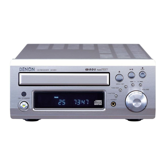
- Page 1 For Europe & U.K. model Version 2 SERVICE MANUAL UD-M31 MODEL STEREO CD RECEIVER Some illustrations using in this service manual are slightly different from the actual set. 16-11, YUSHIMA 3-CHOME, BUNKYOU-KU, TOKYO 113-0034 JAPAN Telephone: 03 (3837) 5321 X0164V.02 DE/CDM 0302...
-
Page 2: Top Cover
UD-M31 SAFETY PRECAUTIONS The following check should be performed for the continued protection of the customer and service technician. LEAKAGE CURRENT CHECK Before returning the unit to the customer, make sure you make either (1) a leakage current check or (2) a line to chassis resistance check. -
Page 3: Rear Panel
UD-M31 4. REAR PANEL Cord Bush Pull out the cord bush. Remove 12 screws ⑥ 5. MAIN PWB Connector Remove 4 screws ⑦ fixing the radiator the chas- sis. Unplug 3 connectors on the AMP PWB. Detach the Main PWB together with the radiator . -
Page 4: Block Diagram
UD-M31 BLOCK DIAGRAM TUNER MODULE IC303 LC72720NM RDS(E2/EK only) IC301 BU4066BCF REC out REC OUT SEL IC801 LA6559 IC803 DRIVER MECHA LC78625E REC out IC302 CD DSP IC802 LC75432M CD11FTA3N LA9241 SELECTOR & VR & EQ IC805 IC804 RF AMP... -
Page 5: Level Diagram
UD-M31 LEVEL DIAGRAM 0dB=0.55V UNIT FUNCTION SWITCH MASTER VOLUME TONE/SDB POWER AMP UNIT +4dB BUFFER BUFFER RELAY LINE 1 LINE 2 ANALOG SWITCH 4066 MUTE LINE 1 LINE 2 LC75342M PRE OUT (dBV) +16dB 15W/6 9.49V 0dB play back CD=1.1V +0.83dB... -
Page 6: Cd Test Mode
UD-M31 CD TEST MODE Setting of the test mode and explanation of each button ITEM OPERATION FUNCTION DISPLAY 1.This service mode starts 1.Display "01" Plug the AC cord to the wall outlet while push- Start the mode 2.Pick up moves to the 10mm 2.The PLAY and the PAUSE... - Page 7 UD-M31 How to check the test mode ( 1 ) DISC discrimination, adjustment * Insert DISC, and press the AUTO SEARCH REVERSE button. * “06 Adj” is displayed, and discrimination of DISC size 8 cm/12 cm, discrimination of DISC reflectance (CD, CD- R/CD-RW), adjustment of focus, tracking offset, and EF balance will be performed.
- Page 8 UD-M31 WAVE-FORMS OF EACH POINT When 12 cm DISC When 12 cm DISC stop start When 8 cm DISC When 8 cm DISC stop start During PAUSE When focus servo on Track search Track search (when forward) (when reverse) During PLAY...
- Page 9 P00/INTP0 REMOCON Remote-control receive data input RECIEVER P01/INTP1 50/60 50/60Hz AC input RECIEVER P02/INTP2/NMI /DB RXD DENON BUS Data input (interrupt input) RECIEVER P03/INTP3 PROTECT Speaker Terminal DC voltage detect signal input RECIEVER P04/INTP4 SEL.EEPROM EEPROM chip enable output RECIEVER...
- Page 10 P23/PCL Pull up RECIEVER P24/BUZ /RDSRST RDS IC reset output RECIEVER P25/SI0/SDA0 DB RXD DATA BUS for DENON BUS Data input RECIEVER P26/SO0 DB TXD DATA BUS for DEON BUS Data output RECIEVER P27/SCK0/SCL0 DB CLK DENON BUS Clock output...
- Page 11 UD-M31 outputs of Port Symbol Function RECIEVER or CD standby&Defoult P67/ASTB Not used :NC OTHER Positive power OTHER P100/TI5/TO5 OPEN CD mecha. Open P101/TI6/TO6 CLOSE CD mecha. Close P102/TI7/TO7 NC OTHER P103/TI8/TO8 NC OTHER P30/TO0 CD-DSP serial communication read / write...
- Page 12 UD-M31 LC78625E(IC803) SQOUT AS DEPC /P2 CO IN AS DFIN/P1 CQCK AS DACK /P0 TS T10 TST11 DAC KO LASER DFOLO DFORO 4.2M LRCKO CONT EMPH TEST5 TE ST4 DEMO XOUT TE ST3 TEST1 THLD 9 10 11 12 13 14 15 16 17 18 19 20 21 22 23 24 RAM address 2k ´...
- Page 13 UD-M31 LC78625E Terminal Function Pin No. Symbol Function DEFI Defect detection signal (DEF) input (This pin must be connected to 0 V if unused.) Test input. A pull-down resistor is built in. (This pin must be connected to 0 V in normal operation.)
- Page 14 UD-M31 Pin No. Symbol Function LRSY L/R clock output Inverted polarity clock output(during CK2CON Bit clock output(after reset) ROMXA application mode) output signals ROMXA Interpolation data output(after reset) ROM data output (during ROMXA mode) C2 flag output MUTEL Left channel mute output...
- Page 15 UD-M31 LC75725E(IC401) 48 47 46 45 44 43 42 41 40 39 38 37 36 35 34 33 32 S25 OSC0 OSC1 1 2 3 4 5 6 7 8 9 10 11 12 13 14 15 16 DIGIT SEGMENT DRIVER...
- Page 16 UD-M31 LA9241M(IC802) RF DET FIN2 FIN2 FIN1 FIN1 DGND -com DGND INTER FACE TESI RFSM RFSM SLOF RF Amp TESI T. SERVO & T.LOGIC SLOF TOFF TOFF JP + SPINDLE F.SERVO & F.LOGIC SLED SERVO SERVO 20 21 22 23 24 25 26...
- Page 17 UD-M31 Pin No. Symbol Contents Input pin for tracking jump signal from DSP. Input pin for tracking jump signal from DSP. Input pin for tracking gain control signal from DSP. Gain is low when TGL is high. TOFF Input pin for tracking off control signal from DSP. Tracking servo is off when TOFF is high.
- Page 18 UD-M31 LA6559(IC801) Name Function Thermal 5CH output change terminal, logic input of Shutdown loading block Signal System VCC Signal System GND S-VCC S-GND signal system power supply Input Input S-Vcc Power Supply Power Supply (Forward/Reverse/ (For rd/Reverse/ (LOADING) (LOADING) (BTL-AMP:CH1~4)
- Page 19 UD-M31 LC75342M(IC302) VREF TEST LOUT ROUT LBASS2 RBASS2 LBASS1 RBASS1 LTRE RTRE LSELO RSELO ROUT RBASS2 RBASS1 RTRE RSELO RVref CONTROL CIRCUIT LOGIC INTERFACE CIRCUIT CONTROL LVref CIRCUIT TEST LOUT LBASS2 LBASS1 LTRE LSELO LC72720NM(IC303) FLOUT CIN VREF Vddd Vdda...
-
Page 20: Front View
UD-M31 STK402-050(IC501) TR11 TR15 TR14 FRONT VIEW TR12 TR10 TR13 TR16 12 7 6 10 11 14 15 BA6287F(IC805) 93LC66(IC202) DUMMY BIT DATA REGISTER INSTRUCTION REGISTER R/W AMPS INSTRUCTION ADDRESS DECODE DECODER MEMORY ARRAY REGISTER CONTROL Vcc RANGE 256/512 X 8... -
Page 21: Pin Connection
UD-M31 FL DISPLAY HNA-11SS47T (FL401) GRID ASSIGNMENT [11G~2G] PIN CONNECTION PIN NO. 5 4 3 2 1 CONNECTION F NOTE 1) Fin ---- Filament pin 2) nG ---- Grid pin 3) Pn ---- Anode pin 4) NP ---- No pin... - Page 22 UD-M31 PRINTED WIRING BOARD 1U-3498 MAIN UNIT Ass'y COMPONENT SIDE Parts List...
- Page 23 UD-M31 1U-3498 MAIN UNIT Ass'y FOIL SIDE Parts List...
-
Page 24: Component Side
UD-M31 1U-3507 CD UNIT ASS'Y Parts List R927 C923 COMPONENT SIDE FOIL SIDE... -
Page 25: Note For Parts List
UD-M31 NOTE FOR PARTS LIST Part indicated with the mark " " are not always in stock and possibly to take a long period of time for supplying, or in some case supplying of part may be refused. When ordering of part, clearly indicate "1" and "I" (i) to avoid mis-supplying. - Page 26 UD-M31 PARTS LIST OF P.W.B. UNIT ASS'Y 1U-3498 MAIN UNIT ASS'Y Ref. No. Part No. Part Name Remarks Q’ty SEMICONDUCTORS GROUP IC201 262 3180 208 UPD784216AGC-203-8EU IC202 262 2986 005 93LC66 IC203 263 1093 002 BA05ST IC205 263 0454 901...
- Page 27 UD-M31 1U-3498 MAIN UNIT ASS'Y Ref. No. Part No. Part Name Remarks Q’ty D614 276 0375 905 1N4148T77 (TAPE) D615,616 276 0772 003 1N4004 D617-619 276 0375 905 1N4148T77 (TAPE) D621,622 276 0375 905 1N4148T77 (TAPE) D623-626 276 0772 003...
- Page 28 UD-M31 1U-3498 MAIN UNIT ASS'Y Ref. No. Part No. Part Name Remarks Q’ty R345 247 2006 960 RM73B--471JT R347,348 247 2007 943 RM73B--102JT R349,350 247 2012 925 RM73B--104JT R351,352 247 2007 969 RM73B--122JT R353,354 247 2009 909 RM73B--472JT (1608) R355,356...
- Page 29 UD-M31 1U-3498 MAIN UNIT ASS'Y Ref. No. Part No. Part Name Remarks Q’ty R921-923 247 2009 983 RM73B--103JT CAPACITORS GROUP C201 254 4538 900 CE04W1C100MT SMG/RE3 C202,203 257 0511 904 CK73F1H103ZT C204 254 4524 943 CE04W1H010MT SMG/RE3 C208 257 0512 903...
- Page 30 UD-M31 1U-3498 MAIN UNIT ASS'Y Ref. No. Part No. Part Name Remarks Q’ty C505,506 257 0508 917 CC73CH1H471JT C509,510 254 4525 735 CE04W1H221MC SMG/RE3 C511,512 256 1058 971 CF93A1H104JT (JL) C513,514 254 4524 985 CE04W1H100MT SMG/RE3 C515,516 257 0502 955...
- Page 31 UD-M31 1U-3498 MAIN UNIT ASS'Y Ref. No. Part No. Part Name Remarks Q’ty CX72 205 0535 086 7P CONN.BASE CX81 205 0355 088 8P KR CON BASE(L) CX121 205 0375 026 12P CONN.BASE(KR-PH) CX143 205 0708 033 14P CONN.SOCKET CX151...
- Page 32 UD-M31 1U-3498 MAIN UNIT ASS'Y Ref. No. Part No. Part Name Remarks Q’ty 415 0908 003 SHIELD PLATE 449 0172 007 SENSOR HOLDER 461 1110 000 FL SPACER(D-SIDE) 471 3304 015 3X8 CBS-Z...
- Page 33 UD-M31 1U-3507 CD PWB UNIT ASS'Y Ref. No. Part No. Part Name Remarks SEMICONDUCTORS GROUP IC801 263 1091 907 LA6559 IC802 263 1090 005 LA9241M IC803 262 2903 004 LC78625E IC804 263 0934 900 BA4510F-E2 IC805 263 0994 908 BA6287F-E2...
- Page 34 UD-M31 1U-3507 CD PWB UNIT ASS'Y Ref. No. Part No. Part Name Remarks R852 247 2010 985 RM73B--273JT R853 247 2010 972 RM73B--243JT R854 247 2002 964 RM73B--100JT R855 247 2004 991 RM73B--910JT R856 247 2011 942 RM73B--473JT R857 247 2004 991...
- Page 35 UD-M31 1U-3507 CD PWB UNIT ASS'Y Ref. No. Part No. Part Name Remarks C816 254 4196 928 CE04W1HR33MT (SRA) C817 257 0501 927 CK73B1H153KT C818 257 0501 901 CK73B1H103KT (1608) C819 257 0517 908 CK73B1C473KT C820 257 0516 954 CK73B1E104KT...
- Page 36 UD-M31 1U-3507 CD PWB UNIT ASS'Y Ref. No. Part No. Part Name Remarks C899 257 0512 903 CK73F1E104ZT C901,902 257 0507 950 CC73CH1H271JT C903,904 254 4541 913 CE04W1E220MT SMG/RE3 C905,906 257 0509 929 CK73B1H102KT C908 254 4536 915 CE04W1A470MT SMG/RE3...
-
Page 37: Exploded View
UD-M31 EXPLODED VIEW WARNING: Parts List Parts marked with this symbol have critical characteristics. Use ONLY replacement parts recommended by the manufacturer. -
Page 38: Parts List Of Exploded View
UD-M31 PARTS LIST OF EXPLODED VIEW Note: The symbols in the column “Remarks” indicate the following destinations. E2: Europe model EK: U.K. model Ref. No Part No Part Name Remarks Q'ty 1U-3498 MAIN PWB UNIT POWER UNIT AMP1 UNIT AMP2 UNIT... - Page 39 UD-M31 Ref. No Part No Part Name Remarks Q'ty 513 3901 000 LASER CAUTION LABEL 203 4804 034 3P PH-PH SHIELD WIRE CX34 203 8533 000 5P PH-PH CON.CORD CX52 204 0567 006 6P PH-PH CON.CORD CX61 009 0241 015...
-
Page 40: Parts List Of Cd Mechanism Unit
UD-M31 EXPLODED VIEW OF CD MECHANISM UNIT (CD11FTA3N) PARTS LIST OF CD MECHANISM UNIT Ref. No. Part No. Part Name Remarks Q'ty Ref. No. Part No. Part Name Remarks Q'ty 1 964 0009 006 Frame chassis 11 964 0010 008 Mecha lifter... -
Page 41: Packing View
UD-M31 PACKING VIEW PACKING LIST OF PACKING & ACCESSORIES Note: The symbols in the column “Remarks” indicate the following destinations. E2:Europe model EK: U.K. model Ref. No. Part No. Part Name Remarks Q’ty 505 0038 030 POLY COVER 511 3982 007... - Page 42 UD-M31 WIRING AC CORD TUNER 1U-3498-1 POWER UNIT PACK CX032 CY042 CX033 1U-3498-3 CY152 I/O UNIT CY081 CY051 CX031 CX034 1U-3498-8 SP UNIT CX038 CX042 CX121 CX052 CX153 1U-3507 CD PWB UNIT CX052 CX072 CX162 CX251 CX081 1U-3498-7 CD MECHA...
-
Page 43: Note For Schematic Diagram
UD-M31 NOTE FOR SCHEMATIC DIAGRAM WARNING: Parts marked with this symbol have criticalchar- acteristics. Use ONLY replacement parts recommended by themanu- facturer. CAUTION: Before returning the unit to the customer, make sure you- make either (1) a leakage current check or (2) a line to chassis resistance check. - Page 44 UD-M31 SCHEMATIC DIAGRAMS (1/2) TO 1U-3529 V MUTE OUT TO 1U-3529 V MUTE IN R509,510 :100(FR) TO 1U-3529 Vcc GND TO 1U-3529 HP OUT REMOTE TO 1U-3529 SIGNAL LINE SCHEMATIC DIAGRAMS (1/2) 1U-3498-1 POWER UNIT 1U-3498-2 µCON UNIT 1U-3498-3 I/O UNIT...
- Page 45 UD-M31 SCHEMATIC DIAGRAMS (2/2) +5V_D1 R927 C923 220/10 OPEN SIGNAL LINE SCHEMATIC DIAGRAMS (2/2) CD PWB UNIT...
Need help?
Do you have a question about the UD-M31 and is the answer not in the manual?
Questions and answers