
Related Manuals for Caen V2495


Summary of Contents for Caen V2495
- Page 1 CAEN Electronic Instrumentation Tools for Discovery User Manual UM5175 V2495/VX2495 VME Programmable Logic Unit Rev. 1 - October 11 , 2018...
-
Page 2: Purpose Of This Manual
Purpose of this Manual This document contains the full hardware and software description of the V2495/VX2495 VME Programmable Logic Unit. Change Document Record Date Revision Changes August 01 , 2016 Initial release October 11 , 2018 Removed “Coming Soon” from the User Firmware FW2495SC in Tab. - Page 3 The information contained herein has been carefully checked and is believed to be accurate; however, no responsibility is assumed for inaccuracies. CAEN SpA reserves the right to modify its products specifications without giving any notice; for up to date information please visit www.caen.it.
-
Page 4: Table Of Contents
Configuration ROM (0x8100-0x81FF) .........................37 Configuration and Status Registers (0x8200-0x83FF) ...................38 MFPGA Firmware Revision Register ..........................38 Software Reset Register ..............................38 Scratch Register ................................38 Flash Configuration (0x8500-0x8AFF)........................38 Internal Scratch SRAM(0x8C00-0x8FFF) ........................38 10 Firmware Development....................39 UM5175 – V2495/VX2495 User Manual rev. 1... -
Page 5: List Of Figures
Fig. 3.2: The UFPGA and GDG interface............................12 Fig. 4.1: Front panels view ................................13 Fig. 5.1: On-board internal connectors and LEDs ..........................16 Fig. 7.1: V2495 motherboard with mezzanine boards ........................22 Fig. 7.2: Multi-pin connector pin assignment ..........................23 Fig. 7.3: CAEN A967 Cable Adapter ..............................23 Fig. -
Page 6: List Of Tables
CAEN Electronic Instrumentation List of Tables Tab. 1.1: Comparison table between V1495 and V2495 ........................8 Tab. 1.2: Table of models and related items .............................9 Tab. 6.1: V2495/VX2495 specifications table ..........................19 Tab. 6.2: A395A Mezzanine specifications table..........................19 Tab. 6.3: A395B Mezzanine specifications table..........................20 Tab. -
Page 7: Safety Notices
Electronic Instrumentation Safety Notices CAUTION: this product may need proper cooling. USING V2495 WITH MEZZANINE BOARDS MAY REQUIRE CRATES WITH FORCED COOLING AIR FLOW SINCE OVERHEATING MAY DAMAGE THE MODULE (refer to Chap. 6) CAUTION: this product needs proper handling. -
Page 8: Introduction
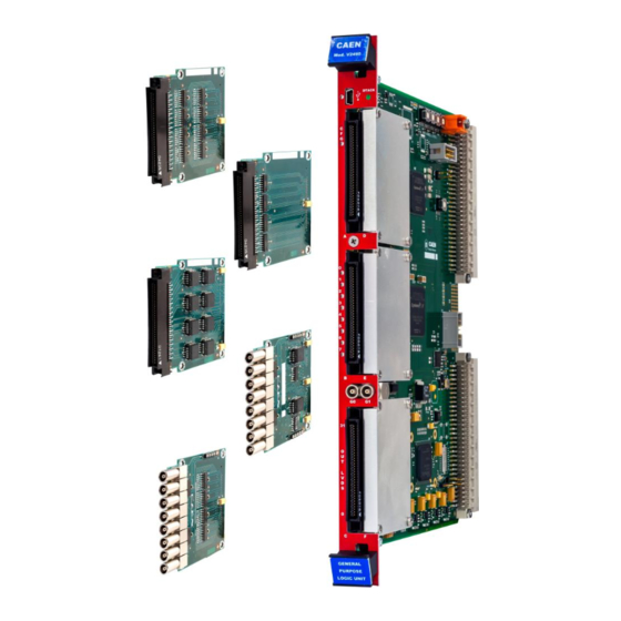
UFPGA through an internal local bus. The presence of three expansion slots interfaced to the UFPGA allows to extend the channel interface of the V2495 by adding up to three independent mezzanine boards. Five mezzanine board types are available: A395A, A395B, A395C, A395D, A395E (see Tab. -
Page 9: Tab. 1.2: Table Of Models And Related Items
WA395XEAAAAA A967 32 Channel Cable Adapter (1x32 to 2x16) WA967XAAAAAA Tab. 1.2: Table of models and related items ⁽*⁾ Paid firmware; unlocking license needed. Please, refer to the FW2495SC web page for details. UM5175 – V2495/VX2495 User Manual rev. 1... -
Page 10: Block Diagram
CAEN Electronic Instrumentation 2 Block Diagram USER LOCAL PROGRAMMABLE MAIN FPGA (MFPGA) FPGA 16 bit (UFPGA) Gate and Delay Generator Fig. 2.1: Block diagram UM5175 – V2495/VX2495 User Manual rev. 1... -
Page 11: Main Components And Interconnections
B PORT (IN) / (Cyclone V GX) E PORT (IN/OUT) AD9520 FLASH G PORT (IN/OUT) FLASH 50 MHz C PORT (OUT) / Gate and Delay F PORT (IN/OUT) Generator Fig. 3.1: Main components and interconnections UM5175 – V2495/VX2495 User Manual rev. 1... -
Page 12: Usb Interface
3.5 Gate and Delay Generator The V2495 hosts a Gate and Delay Generator (see Fig. 3.2) able to provide up to 32 gated and delayed signals (“delayed signals”) triggered by 32 inputs (“start signals”). The gate width and delay value are user programmable. The GDG is an external component implemented in a Xilinx Spartan-6 FPGA. -
Page 13: Front Panel Connectors, Leds And Labels
‘B’ CONNECTOR (32-ch input only) USER CONFIGURATION LEDs G0, G1 CONNECTORS (Input/Output selectable) ‘C’ CONNECTOR (32-ch output only) Fig. 4.1: Front panels view V2495 and VX2495 have the same front panel and connectors. UM5175 – V2495/VX2495 User Manual rev. 1... - Page 14 CAEN Electronic Instrumentation USB PORT FUNCTION MECHANICAL SPECS MiniUSB connector to communicate with the Series: miniUSB connectors. V2495 by USB link for board configuration and Type: SD-54819-026 (B-type). firmware upgrade. Manufacturer: Molex Inc. ELECTRICAL SPECS CABLES N.A. A 1-m USB standard cable is included with the V2495 (USB A-type to miniUSB B-type).
- Page 15 Two blue labels on each insertion/extraction handle of the VME front panel report: − Manufacturer name and board’s model − Brief functional description The label at the bottom of the front panel reports the 4-digit Serial Number (S/N) information. UM5175 – V2495/VX2495 User Manual rev. 1...
-
Page 16: Internal Connectors And Leds
5 Internal Connectors and LEDs MFPGA JTAG MEZZANINE SOCKETS MFPGA CONF_DONE LED UFPGA CONF_DONE LED UFPGA JTAG GDG CONF_DONE LEDs G-PORT TERMINATION SWITCHES POWER SUPPLY LEDS Fig. 5.1: On-board internal connectors and LEDs UM5175 – V2495/VX2495 User Manual rev. 1... - Page 17 50-Ω termination according to the input or output direction and the NIM or TTL configuration relevant connector. • Position “ON” = 50 Ω termination enabled • Position “OFF” = termination disabled UM5175 – V2495/VX2495 User Manual rev. 1...
- Page 18 • SX LED on (orange): FPGA not programmed. POWER SUPPLY LEDs FUNCTION COLOR Two LEDs, placed under the Gate and Green. Delay Generator, light up if the 3.3V power supply for the digital circuitry is provided. UM5175 – V2495/VX2495 User Manual rev. 1...
-
Page 19: Technical Specifications
CAEN Electronic Instrumentation 6 Technical Specifications V2495/VX2495 Motherboard 1-unit wide, 6U high VME64 (V2495) and VME64X (VX2495) FORM FACTOR Nr. of Channels Logic Bandwidth Direct 200 MHz Front Panel Connector Direction Signal Robinson Nugent P50E-068-P1-SR1-TG Input Differential LVDS/ECL/PECL I/O SECTIONS A and B... -
Page 20: Tab. 6.3: A395B Mezzanine Specifications Table
+12V and -12V rails are not used Tab. 6.6: A395E Mezzanine specifications table A395C A395D OPERATING THE V2495 WITH MORE THAN ONE MEZZANINE BOARDS REQUIRES USING VME CRATES WITH FORCED COOLING AIR FLOW SINCE OVERHEATING DUE TO INSUFFICIENT VENTILATION MAY DAMAGE THE MODULE. -
Page 21: Getting Started With V2495
V2495 Programmable VME Logic Unit Without mezzanine board With mezzanine board extension(s) extension(s), according to the order⁽¹⁾ USB cable V2495 User Manual ⁽¹⁾ Mezzanine boards are available by ordering option (refer to Tab. 1.2). UM5175 – V2495/VX2495 User Manual rev. 1... -
Page 22: Mezzanine Boards Installation
Electronic Instrumentation 7.2 Mezzanine Boards Installation In order to install an A395x-series mezzanine board on the V2495 motherboard, please use a Phillips screwdriver. • Remove (unscrew) the metal cover of one of the available mezzanine slots. • Plug the mezzanine board into the 100-pin expansion connector on the motherboard (see Chap. 5) •... -
Page 23: Front Panel Connector Cabling
Fig. 7.2: Multi-pin connector pin assignment The CAEN A967 Cable Adapter (Fig. 7.3) allows to adapt each Robinson Nugent multi-pin connector into two 1” 17+17- pin Header-type male connectors (3M, 4634-7301) with locks through two 25 cm long flat cables. Refer to the cable datasheet [RD3] for specifications and to Tab. -
Page 24: Setting The Vme Base Address
Position 4 = Gate and Delay Demo (see Sect. Gate and Delay Demo Description) Position 5 = available (empty) Note: All the positions from 6 up to 15 are equivalent to position 0: factory firmware is loaded. UM5175 – V2495/VX2495 User Manual rev. 1... -
Page 25: Power-On Configuration Sequence
• If the UFPGA Configuration LED is off and the SW5 selector is set to position 0 or the GDG Configuration LED lights up orange, please contact CAEN for further instructions. Refer to Chap. 12 for CAEN Support contacts. -
Page 26: Driver And Software Installation
Note: to ensure the best system performance, it is recommended to have always the latest drivers release installed. Direct USB Driver In order to communicate with the V2495 through the front panel USB interface (see Chap. 4), the related driver can be downloaded from the V2495 webpage in the Software/Firmware tab (login required). -
Page 27: Fig. 8.2: Usb Driver Manual Installation: Step1
CAEN Electronic Instrumentation 4. Right click on “V2495” item and select Update Driver Software option in the slide menu. Fig. 8.2: USB driver manual installation: Step1 5. Select Browse my computer for driver software as in Fig. 8.3. Fig. 8.3: USB driver manual installation: Step2... -
Page 28: Fig. 8.4: Usb Driver Manual Installation: Step3
6. Use the [Browse] button to point to the driver folder in the destination path on the host PC. Fig. 8.4: USB driver manual installation: Step3 7. Click the [Close] button at the end of the installation process. Fig. 8.5: USB driver manual installation: Step4 UM5175 – V2495/VX2495 User Manual rev. 1... -
Page 29: Vme Access
V2495 is fully supported by Linux kernels from kernel version 3.13 on. VME Access The V2495 can be accessed through the VME bus. CAEN provides a USB-to-VME bridge (mod. V1718) and a CONET-to- VME CAEN Bridge (mod. V2718). ➢ V1718 USB Driver The required driver can be downloaded from the V1718 web page in the Software/Firmware tab (login required) and manually installed. -
Page 30: Software Tools
Get the Board Info file (useful in case of support requests) CAENUpgrader can operate with Windows and Linux, 32 and 64-bit OSs The software installation package can be downloaded from the CAEN web site (login required) at: Home / Products / Firmware/Software / Digitizer Software / Configuration Tools / CAENUpgrader For any installation and functions which are not described in this manual, please refer to the software Quick Start Guide, [RD1]. -
Page 31: Fig. 8.8: Caenupgrader Mfpga Upgrade Firmware Menu
Electronic Instrumentation ➢ Upgrade the V2495 Main FPGA Firmware The MFPGA firmware is available on CAEN website at the V2495 web page (login required): Home / Products / Modular Pulse Processing Electronics / VME / I/O Registers / V2495 The firmware file is available in Altera RPD format. -
Page 32: Fig. 8.9: Caenupgrader Ufpga Flash Memory Image Menu
7. Press the Upgrade button. The outcome of the upgrade process is shown in a message window (see Fig. 8.10). At the end of the upgrade process, the CAEN Upgrader will force a reconfiguration of the UFPGA from the application image selected by the rotary switch (see Fig. -
Page 33: Plulib Library
Electronic Instrumentation PLULib Library CAEN PLULib library is a library of C functions developed to control V2495/VX2495 and DT5495 programmable logic units through direct USB and Ethernet communication interfaces, but also through the VMEbus connection by using CAEN Bridges (V2718 and V1718), if supported. -
Page 34: Communication Interfaces
CAEN Electronic Instrumentation 9 Communication Interfaces The V2495 board can be accessed via both VME bus or USB interface. All registers are accessible from both communication interfaces (VME/USB). 9.1 VME Bus The V2495/VX2495 boards can be individually addressed on the bus by means of their assigned base address. -
Page 35: Address Map
CAEN Electronic Instrumentation 9.3 Address Map The following table illustrates the V2495 address map: Address Description BA + 0x0000-0x0FFF UFPGA data access BA + 0x1000-0x7FFF UFPGA register access BA + 0x8000-0x80FF VME Interface Registers BA + 0x8100-0x81FF Configuration ROM BA + 0x8200-0x83FF... -
Page 36: Vme Interface Registers (0X8000-0X80Ff)
VME Base Address Register Description This register allows to read the value of on-board rotary switches (see Fig. [31:0] 7.4). It is meant to be used from the USB interface for testing purposes UM5175 – V2495/VX2495 User Manual rev. 1... -
Page 37: Configuration Rom (0X8100-0X81Ff)
Serial Number (LSB) Tab. 9.3: ROM Address Map of the V2495 Note: The oui0/1 fields represent CAEN Manufacturer identifier (IEEE OUI), which is equal to 0x40E6. Note: The version field identifies the module version (V2495/VX2495). Note: The board serial number can be read with two accesses: if the serial number on the module front panel is 1245 ... -
Page 38: Configuration And Status Registers (0X8200-0X83Ff)
Note: access to the FLASH is through the provided functions of the PLULib library (see Sect. Software Tools). Internal Scratch SRAM(0x8C00-0x8FFF) This area is available either for test access or for volatile data storage. Any address in this interval is implemented by an internal RAM location. UM5175 – V2495/VX2495 User Manual rev. 1... -
Page 39: Firmware Development
The four demos provided in the UFPGA flash memory will also be discussed: a step-by-step guide will be given to run the examples. Their goal is to provide an extensive overview of the main functionalities of the V2495 board and of its mezzanine cards. -
Page 40: User Fpga I/O Ports
TTL case: It is up to the firmware to handle this inversion, for example using the SELG signal to invert the logic level as shown in the following VHDL assignment: GIN_MOD <= GIN[0] when SELG=’1’ else not GIN[0]; UM5175 – V2495/VX2495 User Manual rev. 1... -
Page 41: Fig. 10.1: Simplified Scheme Related To Tab. 10.5
• A395D channel 0 can be driven with signal X[0] and its status can be read from X[2]. • A395D channel 1 can be driven with signal X[16] and its status can be read from X[18]. UM5175 – V2495/VX2495 User Manual rev. 1... -
Page 42: Tab. 10.6: Led Ports Description Table
Last cycle (active low) Write/Read cycle Input 0 = read 1 = write nADS Input Address strobe (active low) nREADY Output Slave ready/Prefetch request Input/Ou Data/address bus tput Tab. 10.8: Local Bus ports description table UM5175 – V2495/VX2495 User Manual rev. 1... -
Page 43: Local Bus Interface
LBS. Fig. 10.2: Local bus signals at a write access (x8BADF00D is written on register x1800) Fig. 10.3: Local bus signal at a read access (x8BADF00D is read from register x1800) UM5175 – V2495/VX2495 User Manual rev. 1... -
Page 44: Fig. 10.4: Prefetch Mechanism
0x0000 (fixed). The User logic is required to respond only to address 0x0000: data from its data queue are made available to the V2495 local bus. If a new register access is requested to the local bus master while a prefetch cycle is ongoing, the prefetch cycle will be interrupted by asserting the nBLAST signal and the register access will be served with priority. -
Page 45: Gate And Delay Controller
Example 3: If the delay value is set to 0xFFF8 (≈ 701 µs), the ma maximum possible gate value is 0x8 (typ. 86.9 ns). PARAMETER VALUE 12 ns (typ.) ± 10% 10.7 ns (typ.) ± 10% Tab. 10.9: Main parameters of the Gate and Delay Generator UM5175 – V2495/VX2495 User Manual rev. 1... -
Page 46: Register Description
The UFPGA can set the relevant configuration registers and read data from the generator through the SPI protocol. CAEN does not provide a detailed description of the communication protocol over the SPI bus for GDG configuration. A VHDL component is provided in the gd_control.vhd source code (GD_CONTROL), included in all the user demo firmware. -
Page 47: Example Procedures
Note that in the case of a broadcast command the delay and gate values are serialized to the GDG at the same time. The bits related to the channel index (six LSBs of the CONTROL register) are irrelevant in this case. UM5175 – V2495/VX2495 User Manual rev. 1... -
Page 48: Porting V1495 To V2495
Electronic Instrumentation 10.5 Porting V1495 to V2495 Firmware designs targeted to the V1495 User FPGA can be ported to V2495 by keeping in mind the following differences between the two modules: The V2495 FPGA device is different (Cyclone V versus Cyclone I) and with larger logic resources. While there will be no resource constrains, the FPGA configuration scheme and output binary files are different for the two boards. -
Page 49: Demo Firmware
0). To run a firmware “as it is”, it is required to use the functions of the CAEN PLULib library to access the proper (refer to Sect. Software Tools). To modify the demos and upload the new firmware on the FPGA, a basic knowledge of VHDL language and Altera Quartus II software are required. -
Page 50: Introduction
Input value of Port B ➢ C-PORT VALUE register: Contains the 32 output bits of port C (selectable by the user in this demo). Address: 0x100C. Mode: Read only. Description [31:0] Output value of port C UM5175 – V2495/VX2495 User Manual rev. 1... - Page 51 0x7 = the OR of ports A and B (possibly masked) is captured and sent to C when a gate signal is active 0x8 = a clock counter (@ 50 MHz) is sent to C 0x9/0xF = the value of a register is sent to C UM5175 – V2495/VX2495 User Manual rev. 1...
- Page 52 ➢ C-PORT USER VALUE register: Allows to set the C port value when Control register bits[3:0] are set to 0x9/0xF. Address: 0x180C. Mode: Read and Write. Description [31:0] User value of Port C UM5175 – V2495/VX2495 User Manual rev. 1...
-
Page 53: Introduction
Address: 0x1004. Mode: Read only. Description [31:0] Input on port A ➢ B PORT VALUE: the 32 input bits of port B Address: 0x1008. Mode: Read only. Description [31:0] Input on port B UM5175 – V2495/VX2495 User Manual rev. 1... - Page 54 0 = NIM level 1 = TTL level ➢ C PORT VALUE register: allows to set an arbitrary value to port C. Address: 0x180C. Mode: Read and Write. Description [31:0] User output value for port C UM5175 – V2495/VX2495 User Manual rev. 1...
-
Page 55: Dac Demo Description
The 3 LSBs [18:16] select the channel for either a write or read access. If a write access is [19:16] performed and [19] = 1 all channels are selected for writing; if a read access is performed [19] is ignored [15:0] DAC value UM5175 – V2495/VX2495 User Manual rev. 1... - Page 56 Mode: Read and Write. Description [31:0] DAC value Please, note that the DAC value obtained from register 0x1804 is not read from the chip, but it is the last set value for that specific channel. UM5175 – V2495/VX2495 User Manual rev. 1...
-
Page 57: Introduction
I/O port level selection: 0 = NIM level 1 = TTL level WARNING: When the G0 connector is used as an input, the user should follow the procedure described in Sect. User FPGA I/O ports. UM5175 – V2495/VX2495 User Manual rev. 1... - Page 58 1 = Start of read operation 1 = Start of write operation ➢ DATA READ register: The information from the DFPGA can be read in this register. Address: 0x7F0C. Mode: Read only. Description [31:0] Data UM5175 – V2495/VX2495 User Manual rev. 1...
- Page 59 Gate and delay ready signal (when 0, the Gate and Delay controller is busy. A new command to the Gate and Delay controller should not be issued before this bit sets back to 1) UM5175 – V2495/VX2495 User Manual rev. 1...
-
Page 60: Software Development
CAEN Electronic Instrumentation 12 Software Development Software applications can be developed for the V2495 by using the functions and features provided by the CAEN PLULib library [RD4]. CAEN PLULib library requires the Main FPGA Application Firmware revision 1.4 or higher! -
Page 61: Caen Support
CAEN Electronic Instrumentation 13 CAEN Support CAEN support services are available for the user by accessing the Support & Services area on CAEN website at www.caen.it. 13.1 Returns and Repairs If a product(s) return and repair is needed, a Product Return Form (PRF) should be filled and submitted from the Returns and Repairs area at Home / Support &... - Page 62 Tools for Discovery UMD5175 - V2495/VX2495 User Manual rev. 1 -October 11th, 2018 00100-15-V2495-MUTX Copyright © CAEN SpA. All rights reserved. Information in this publication supersedes all earlier versions. Specifications subject to change without notice. UM5175 – V2495/VX2495 User Manual rev. 1...
Need help?
Do you have a question about the V2495 and is the answer not in the manual?
Questions and answers