
Related Manuals for Caen DT5495


Summary of Contents for Caen DT5495
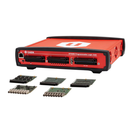
- Page 1 CAEN Electronic Instrumentation Tools for Discovery User Manual UM6508 DT5495 Desktop Programmable Logic Unit Rev. 0 - August 2 , 2018...
-
Page 2: Purpose Of This Manual
Purpose of this Manual This document contains the full hardware and software description of the DT5495 Desktop Programmable Logic Unit. Change Document Record Date Revision Changes August 2 , 2018 Initial release Symbols, Abbreviated Terms and Notation Address Modifier Ethernet Interface... - Page 3 The information contained herein has been carefully checked and is believed to be accurate; however, no responsibility is assumed for inaccuracies. CAEN SpA reserves the right to modify its products specifications without giving any notice; for up to date information please visit www.caen.it.
-
Page 4: Table Of Contents
10.2 User FPGA I/O ports ..........................39 10.3 Local Bus Interface ..........................42 10.4 Gate and Delay Controller ........................44 General Description ................................44 Register Description ...............................45 Example Procedures ..............................46 10.5 Porting V1495 to DT5495 ........................47 UM6508 – DT5495 User Manual rev. 0... -
Page 5: List Of Figures
Fig. 8.9: Ethernet Properties window” ..............................29 Fig. 8.10: Properties window of the ”Internet Protocol Version (TPC/IPv4)” ................29 Fig. 8.11: Instrument Information page of the DT5495 Web Interface ..................30 Fig. 8.12: Instrument Information page of the DT5495 Web Interface ..................30 Fig. 8.13: CAENUpgrader Get Firmware Release menu ......................31 Fig. - Page 6 Tab. 5.5: A395D Mezzanine specifications table ...........................18 Tab. 5.6: A395E Mezzanine specifications table..........................18 Tab. 9.1: DT5495 register address map ............................35 Tab. 9.2: ROM Address Map of the DT5495 ..........................36 Tab. 9.3: CSR registers ..................................36 Tab. 10.1: Clock ports description table ............................39 Tab.
-
Page 7: Introduction
DT5495 by adding up to three independent mezzanine boards. Five mezzanine board types are available: A395A, A395B, A395C, A395D, A395E (see Tab. 1.2). The DT5495 can reach a maximum of 194 I/O channels. The board can be controlled and programmed through either the Ethernet or the USB interface. The CAENUpgrader software tool is provided to upload the FPGA firmware, while a dedicated C library is available to support the custom software development. -
Page 8: Tab. 1.2: Table Of Models And Related Items
Board Models Description Product Code DT5495 Desktop Programmable Logic Unit WDT5495XAAAA User Firmware Description Product Code FW2495SC⁽*⁾ Channel Latching Scaler for V2495 and DT5495 WFW2495SCXAA Accessories Description Product Code A395A 32 LVDS/ECL/PECL input channels WA395XAAAAAA A395B 32 LVDS output channels... -
Page 9: Block Diagram
CAEN Electronic Instrumentation 2 Block Diagram USER LOCAL PROGRAMMABLE MAIN FPGA (MFPGA) FPGA 16 bit (UFPGA) Gate and Delay Generator Fig. 2.1: Block diagram UM6508 – DT5495 User Manual rev. 0... -
Page 10: Main Components And Interconnections
B PORT (IN) / (Cyclone V GX) E PORT (IN/OUT) AD9520 FLASH G PORT (IN/OUT) FLASH 50 MHz C PORT (OUT) / Gate and Delay F PORT (IN/OUT) Generator Fig. 3.1: Main components and interconnections UM6508 – DT5495 User Manual rev. 0... -
Page 11: Usb Interface
3.5 Gate and Delay Generator The DT5495 hosts a Gate and Delay Generator (see Fig. 3.2) able to provide up to 32 gated and delayed signals (“delayed signals”) triggered by 32 inputs (“start signals”). The gate width and delay value are user programmable. The GDG is an external component implemented in a Xilinx Spartan-6 FPGA. -
Page 12: Front Panel Connectors, Leds And Labels
‘C’ CONNECTOR USER CONFIGURATION CONFIGURATION USB PORT LEDs (32-ch output only) & ACTIVITY LED ‘JTAG’ CONNECTOR ‘RESTORE’ IDENTIFICATION ON/OFF LABEL BUTTON SWITCH DC IN CONNECTOR Fig. 4.1: front (top) and rear (down) panel view UM6508 – DT5495 User Manual rev. 0... -
Page 13: Front Panel
ELECTRICAL SPECS A 1-m USB standard cable is included with the DT5495 (USB A-type to miniUSB B-type). N.A. USB LED (GREEN): driven by the Main PFGA, this LED lights up if a USB read/write access to the board is performed. - Page 14 See Tab. 5.1. 0, 1, 2, …, 7 LEDs FUNCTION COLOR The status of these LEDs is user-programmable Green. NOTE: when the UFPGA is in Factory mode, odd and even LEDs alternatively blink. UM6508 – DT5495 User Manual rev. 0...
-
Page 15: Rear Panel
JTAG CONNECTOR FUNCTION MECHANICAL SPECS Input connector for the DT5495 Series: DC power Jacks. main power supply from the Type: KLDX-0202-A-LT. external AC/DC adaptor. Manufacturer: KYCON. ELECTRICAL SPECS Input voltage: +12 VDC (typ.). UM6508 – DT5495 User Manual rev. 0... - Page 16 CAEN Electronic Instrumentation ON/OFF SWITCH FUNCTION MECHANICAL SPECS Power switch of the module: Series: Power Switches. on (I) / off (O) Type: Rocker SwitchP (A11131121000) Manufacturer: Molveno. ELECTRICAL SPECS N.A. UM6508 – DT5495 User Manual rev. 0...
-
Page 17: Technical Specifications
Extended Common Mode input range: -4V to +5V Fail Safe input feature 0.1 A (max) @ +5V internal rail POWER CONSUMPTIONS +12V and -12V internal rails are not used Tab. 5.2: A395A Mezzanine specifications table UM6508 – DT5495 User Manual rev. 0... -
Page 18: Tab. 5.3: A395B Mezzanine Specifications Table
LEMO 00 Output 16-bit resolution ±5V @10kΩ RL ±4V @200Ω RL 0.3 A (max) @ +5V internal rail POWER CONSUMPTIONS +12V and -12V internal rails are not used Tab. 5.6: A395E Mezzanine specifications table UM6508 – DT5495 User Manual rev. 0... -
Page 19: Power Requirements
Electronic Instrumentation 6 Power Requirements The DT5495 is powered by the external 45W 12V AC/DC stabilized power supply unit included in the delivered kit (see Sect. Shipping Content). The maximum required current is typically 500mA (without any mezzanine extension). UM6508 – DT5495 User Manual rev. 0... -
Page 20: Getting Started With Dt5495
DT5495 Programmable VME Logic Unit With or without mezzanine board extension(s), according to the order⁽¹⁾ USB cable Ethernet cable Power Supply adaptor DT5495 User Manual ⁽¹⁾ Mezzanine boards are available by ordering option (refer to Tab. 1.2). UM6508 – DT5495 User Manual rev. 0... -
Page 21: Mezzanine Boards Installation
CAEN Electronic Instrumentation 7.2 Mezzanine Boards Installation If you need to install one or more A395x-series mezzanine board on your DT5495, please contact CAEN to receive detailed instructions (see Sect. Technical Support Service). Fig. 7.1: DT5495 motherboard with mezzanine boards... -
Page 22: Front Panel Connector Cabling
Fig. 7.2: Multi-pin connector pin assignment The CAEN A967 Cable Adapter (Fig. 7.3) allows to adapt each Robinson Nugent multi-pin connector into two 1” 17+17- pin Header-type male connectors (3M, 4634-7301) with locks through two 25 cm long flat cables. Refer to the cable datasheet [RD2] for specifications and to Tab. -
Page 23: Power-On Configuration Sequence
Main FPGA firmware, while the ethernet IP address of the board is not affected. 2b. Power cycle the DT5495, then wait for at least 15 seconds; this way, both the IP address is restored to the default value and the board is forced to boot from the factory Main FPGA firmware. -
Page 24: Communication
1. Download and unpack the driver installation package on the host PC. 2. Plug the USB cable on the DT5495 and on the PC. Windows should detect the new hardware. 3. Go to the Device Manager area. The new hardware is listed in Other devices as “V2495” (see Fig. 2.1). -
Page 25: Fig. 8.2: Usb Driver Manual Installation: Step1
4. Right click on “V2495” item and select Update Driver Software option in the slide menu. Fig. 8.2: USB driver manual installation: Step1 5. Select Browse my computer for driver software as in Fig. 8.3. Fig. 8.3: USB driver manual installation: Step2 UM6508 – DT5495 User Manual rev. 0... -
Page 26: Fig. 8.4: Usb Driver Manual Installation: Step3
6. Use the [Browse] button to point to the driver folder in the destination path on the host PC. Fig. 8.4: USB driver manual installation: Step3 7. Click the [Close] button at the end of the installation process. Fig. 8.5: USB driver manual installation: Step4 UM6508 – DT5495 User Manual rev. 0... -
Page 27: Fig. 8.6: Usb Driver Manual Installation: Step5
Fig. 8.6: USB driver manual installation: Step5 ➢ Linux OS DT5495 is fully supported by Linux kernels from kernel version 3.13 on. This means that such kernel versions should be able to recognize the hardware automatically, without requiring the user to install any driver. -
Page 28: Ethernet Configuration
Fig. 8.7: The Network and Sharing Center window Click on ”Change adapter settings”. Right click on the Ethernet icon and select ”Properties” from the slide menu ( Fig. 8.8 Fig. 8.8: Properties window of the Ethernet network UM6508 – DT5495 User Manual rev. 0... -
Page 29: Fig. 8.9: Ethernet Properties Window
IP Address numbers of the Hexagon IP, while make sure to set the fourth decimal number to a value different from the Hexagon one to avoid IP conflicts over the net. It is finally possible to connect to Hexagon by the Web Interface described in the next section (Sec. Web Interface). UM6508 – DT5495 User Manual rev. 0... -
Page 30: Web Interface
8.3 Web Interface Note: Check that the DT5495 is powered on, the Ethernet cable is connected, and the Network is set according to Sect. Ethernet Configuration. Open the web browser and type the DT5495 IP Address as web address. In the default case, the IP Address is 192.168.0.90:... -
Page 31: Software Tools
Get the Board Info file (useful in case of support requests) CAENUpgrader can operate with Windows and Linux, 32 and 64-bit OSs The software installation package can be downloaded from CAEN web site (login required) at the CAENUpgrader web page. -
Page 32: Fig. 8.14: Caenupgrader Mfpga Upgrade Firmware Menu
Electronic Instrumentation ➢ Upgrade the DT5495 Main FPGA Firmware The MFPGA firmware can be downloaded from CAEN website at the DT5495 web page (login required): The firmware file is available in Altera RPD format. The following instructions allow to upgrade the MFPGA firmware: 1. -
Page 33: Fig. 8.15: Caenupgrader Ufpga Flash Memory Image Menu
7. Press the Upgrade button. The outcome of the upgrade process is shown in a message window (see Fig. 8.16). At the end of the upgrade process, the CAEN Upgrader will force a reconfiguration of the UFPGA from the selected user application image. -
Page 34: Plulib Library
Electronic Instrumentation PLULib Library CAEN PLULib library is a library of C functions developed to control V2495/VX2495 and DT5495 programmable logic units through direct USB and Ethernet communication interfaces, but also through the VMEbus connection by using CAEN Bridges (V2718 and V1718), if supported. -
Page 35: Software Interface
CAEN Electronic Instrumentation 9 Software Interface The DT5495 board can be accessed via both Ethernet and USB interface. All registers are accessible from both communication interfaces. 9.1 Address Map The following table illustrates the DT5495 address map: Address Description 0x0000-0x0FFF... -
Page 36: Configuration Rom (0X8100-0X81Ff)
Tab. 9.2: ROM Address Map of the DT5495 Note: The oui0/1 fields represent CAEN Manufacturer identifier (IEEE OUI), which is equal to 0x40E6. Note: The board serial number can be read with two accesses: if the serial number on the module front panel is 1245 ... -
Page 37: Mfpga Firmware Revision Register
Note: access to the FLASH is through the provided functions of the PLULib library (see Sect. Software Tools). Internal Scratch SRAM(0x8C00-0x8FFF) This area is available either for test access or for volatile data storage. Any address in this interval is implemented by an internal RAM location. UM6508 – DT5495 User Manual rev. 0... -
Page 38: Firmware Development
The four demos provided in the UFPGA flash memory will also be discussed: a step-by-step guide will be given to run the examples. Their goal is to provide an extensive overview of the main functionalities of the DT5495 board and of its mezzanine cards. -
Page 39: User Fpga I/O Ports
• The SELx and nOEx signals are meaningful only for the A395D mezzanine card. When this mezzanine is not used, these signals can be left undriven. • Mezzanines with 32 I/O signals have a one-to-one correspondence between physical signals and I/O pins (i.e. X[i] corresponds to the i-th channel of the mezzanine). UM6508 – DT5495 User Manual rev. 0... -
Page 40: Fig. 10.1: Caencomm Demo Java And Labview Graphical Interface
Input SPI MISO (Master Input Slave Output) SPI_SCLK Output Serial clock SPI_CS Output SPI Chip Select SPI_MOSI Output SPI MOSI (Master Output Slave Input) Tab. 10.7: Gate and Delay Generator ports description table UM6508 – DT5495 User Manual rev. 0... -
Page 41: Tab. 10.8: Local Bus Ports Description Table
Last cycle (active low) Write/Read cycle Input 0 = read 1 = write nADS Input Address strobe (active low) nREADY Output Slave ready/Prefetch request Input/Ou Data/address bus tput Tab. 10.8: Local Bus ports description table UM6508 – DT5495 User Manual rev. 0... -
Page 42: Local Bus Interface
LBS. Fig. 10.2: Local bus signals at a write access (x8BADF00D is written on register x1800) Fig. 10.3: Local bus signal at a read access (x8BADF00D is read from register x1800) UM6508 – DT5495 User Manual rev. 0... -
Page 43: Fig. 10.4: Prefetch Mechanism
0x0000 (fixed). The User logic is required to respond only to address 0x0000: data from its data queue are made available to the DT5495 local bus. If a new register access is requested to the local bus master while a prefetch cycle is ongoing, the prefetch cycle will be interrupted by asserting the nBLAST signal and the register access will be served with priority. -
Page 44: Gate And Delay Controller
Example 3: If the delay value is set to 0xFFF8 (≈ 701 µs), the ma maximum possible gate value is 0x8 (typ. 86.9 ns). PARAMETER VALUE 12 ns (typ.) ± 10% 10.7 ns (typ.) ± 10% Tab. 10.9: Main parameters of the Gate and Delay Generator UM6508 – DT5495 User Manual rev. 0... -
Page 45: Register Description
The UFPGA can set the relevant configuration registers and read data from the generator through the SPI protocol. CAEN does not provide a detailed description of the communication protocol over the SPI bus for GDG configuration. A VHDL component is provided in the gd_control.vhd source code (GD_CONTROL), included in all the user demo firmware. -
Page 46: Example Procedures
Note that in the case of a broadcast command the delay and gate values are serialized to the GDG at the same time. The bits related to the channel index (six LSBs of the CONTROL register) are irrelevant in this case. UM6508 – DT5495 User Manual rev. 0... -
Page 47: Porting V1495 To Dt5495
Electronic Instrumentation 10.5 Porting V1495 to DT5495 Firmware designs targeted to the V1495 User FPGA can be ported to DT5495 by keeping in mind the following differences between the two modules: The DT5495 FPGA device is different (Cyclone V versus Cyclone I) and with larger logic resources. While there will be no resource constrains, the FPGA configuration scheme and output binary files are different for the two boards. -
Page 48: Demo Firmware
The wanted demo can be stored only on the application 1 page of the UFPGA FLASH memory. To run a firmware “as it is”, it is required to use the functions of the CAEN PLULib library to access the proper registers (refer to Sect. -
Page 49: Introduction
Input value of Port B ➢ C-PORT VALUE register: Contains the 32 output bits of port C (selectable by the user in this demo). Address: 0x100C. Mode: Read only. Description [31:0] Output value of port C UM6508 – DT5495 User Manual rev. 0... - Page 50 0x7 = the OR of ports A and B (possibly masked) is captured and sent to C when a gate signal is active 0x8 = a clock counter (@ 50 MHz) is sent to C 0x9/0xF = the value of a register is sent to C UM6508 – DT5495 User Manual rev. 0...
- Page 51 ➢ C-PORT USER VALUE register: Allows to set the C port value when Control register bits[3:0] are set to 0x9/0xF. Address: 0x180C. Mode: Read and Write. Description [31:0] User value of Port C UM6508 – DT5495 User Manual rev. 0...
-
Page 52: Introduction
Address: 0x1004. Mode: Read only. Description [31:0] Input on port A ➢ B PORT VALUE: the 32 input bits of port B Address: 0x1008. Mode: Read only. Description [31:0] Input on port B UM6508 – DT5495 User Manual rev. 0... - Page 53 0 = NIM level 1 = TTL level ➢ C PORT VALUE register: allows to set an arbitrary value to port C. Address: 0x180C. Mode: Read and Write. Description [31:0] User output value for port C UM6508 – DT5495 User Manual rev. 0...
-
Page 54: Register Description
The 3 LSBs [18:16] select the channel for either a write or read access. If a write access is [19:16] performed and [19] = 1 all channels are selected for writing; if a read access is performed [19] is ignored [15:0] DAC value UM6508 – DT5495 User Manual rev. 0... - Page 55 Mode: Read and Write. Description [31:0] DAC value Please, note that the DAC value obtained from register 0x1804 is not read from the chip, but it is the last set value for that specific channel. UM6508 – DT5495 User Manual rev. 0...
-
Page 56: Introduction
I/O port level selection: 0 = NIM level 1 = TTL level WARNING: When the G0 connector is used as an input, the user should follow the procedure described in Sect. User FPGA I/O ports. UM6508 – DT5495 User Manual rev. 0... - Page 57 1 = Start of read operation 1 = Start of write operation ➢ DATA READ register: The information from the DFPGA can be read in this register. Address: 0x7F0C. Mode: Read only. Description [31:0] Data UM6508 – DT5495 User Manual rev. 0...
- Page 58 Gate and delay ready signal (when 0, the Gate and Delay controller is busy. A new command to the Gate and Delay controller should not be issued before this bit sets back to 1) UM6508 – DT5495 User Manual rev. 0...
-
Page 59: Software Development
CAEN Electronic Instrumentation 12 Software Development Software applications can be developed for the DT5495 by using the functions and features provided by the CAEN PLULib library [RD3]. CAEN PLULib library requires the Main FPGA Application Firmware revision 1.4 or higher! -
Page 60: Caen Support
CAEN Electronic Instrumentation 13 CAEN Support CAEN support services are available for the user by accessing the Support & Services area on CAEN website at www.caen.it. 13.1 Returns and Repairs If a product(s) return-and-repair is needed, a Product Return Form (PRF) should be filled and submitted from the Returns and Repairs area at Home / Support &... - Page 61 UMD6508 - DT5495 User Manual rev. 0 - August 2nd, 2018 00100-15-V2495-MUTX Copyright © CAEN SpA. All rights reserved. Information in this publication supersedes all earlier versions. Specifications subject to change without notice. UM6508 – DT5495 User Manual rev. 0...
Need help?
Do you have a question about the DT5495 and is the answer not in the manual?
Questions and answers