Sign In
Upload
Manuals
Brands
Caen Manuals
Controller
V2495
User Manuals: Caen V2495 Programmable Logic Unit
Manuals and User Guides for Caen V2495 Programmable Logic Unit. We have
2
Caen V2495 Programmable Logic Unit manuals available for free PDF download: User Manual
Caen V2495 User Manual (62 pages)
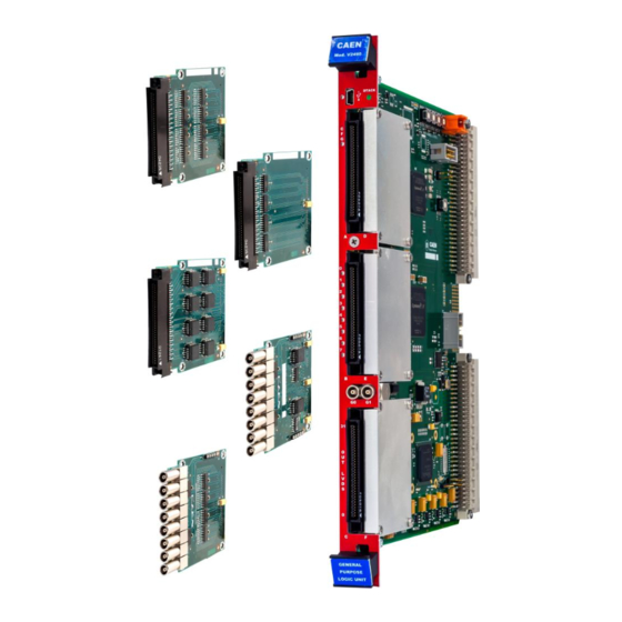
Electronic Instrumentation, VME Programmable Logic Unit
Brand:
Caen
| Category:
Controller
| Size: 2 MB
Table of Contents
Purpose of this Manual
2
Change Document Record
2
Symbols, Abbreviated Terms and Notation
2
Reference Documents
2
Index
4
Table of Contents
4
List of Figures
5
List of Tables
6
Safety Notices
7
1 Introduction
8
Tab. 1.1: Comparison Table between V1495 and V2495
8
Tab. 1.2: Table of Models and Related Items
9
2 Block Diagram
10
Fig. 2.1: Block Diagram
10
3 Main Components and Interconnections
11
Fig. 3.1: Main Components and Interconnections
11
USB Interface
12
VME Interface
12
Main FPGA
12
User FPGA
12
Gate and Delay Generator
12
Clock Distribution
12
Fig. 3.2: the UFPGA and GDG Interface
12
4 Front Panel Connectors, Leds and Labels
13
Fig. 4.1: Front Panels View
13
5 Internal Connectors and Leds
16
Fig. 5.1: On-Board Internal Connectors and Leds
16
6 Technical Specifications
19
Tab. 6.1: V2495/VX2495 Specifications Table
19
Tab. 6.2: A395A Mezzanine Specifications Table
19
Tab. 6.3: A395B Mezzanine Specifications Table
20
Tab. 6.4: A395C Mezzanine Specifications Table
20
Tab. 6.5: A395D Mezzanine Specifications Table
20
Tab. 6.6: A395E Mezzanine Specifications Table
20
7 Getting Started with V2495
21
Shipping Content
21
Mezzanine Boards Installation
22
Fig. 7.1: V2495 Motherboard with Mezzanine Boards
22
Front Panel Connector Cabling
23
Fig. 7.2: Multi-Pin Connector Pin Assignment
23
Fig. 7.3: CAEN A967 Cable Adapter
23
Setting the VME Base Address
24
Selecting the User FPGA Firmware
24
Fig. 7.4: Base Address On-Board Rotary Switches
24
Fig. 7.5: User Firmware Rotary Switch
24
Power-On Configuration Sequence
25
Boot Mode Selection
25
Fig. 7.6: Boot Mode Jumper for the Main FPGA
25
8 Driver and Software Installation
26
Drivers
26
Direct USB Driver
26
Fig. 8.1: V2495 Hardware Detection
26
Fig. 8.2: USB Driver Manual Installation: Step1
27
Fig. 8.3: USB Driver Manual Installation: Step2
27
Fig. 8.4: USB Driver Manual Installation: Step3
28
Fig. 8.5: USB Driver Manual Installation: Step4
28
VME Access
29
Fig. 8.6: USB Driver Manual Installation: Step5
29
Software Tools
30
Caenupgrader
30
Fig. 8.7: Caenupgrader Get Firmware Release Menu
30
Fig. 8.8: Caenupgrader MFPGA Upgrade Firmware Menu
31
Fig. 8.9: Caenupgrader UFPGA Flash Memory Image Menu
32
Fig. 8.10: Caenupgrader UFPGA Upgrade Firmware Menu
32
Plulib Library
33
Fig. 8.11: CAEN Plulib Demo Application Prompt
33
9 Communication Interfaces
34
VME Bus
34
Usb
34
Address Map
35
User FPGA Data Access (0X0000-0X0Fff)
35
User FPGA Register Access (0X1000-0X7Fff)
35
Tab. 9.1: V2495 Register Address Map
35
VME Interface Registers (0X8000-0X80Ff)
36
VME Control Register
36
VME Interrupt Level Register
36
VME Interrupt Status ID Register
36
Scratch Register
36
VME Base Address Register
36
Tab. 9.2: VME Interface Registers
36
Configuration ROM (0X8100-0X81Ff)
37
Tab. 9.3: ROM Address Map of the V2495
37
Configuration and Status Registers (0X8200-0X83Ff)
38
MFPGA Firmware Revision Register
38
Software Reset Register
38
Scratch Register
38
Flash Configuration (0X8500-0X8Aff)
38
Internal Scratch SRAM(0X8C00-0X8Fff)
38
Tab. 9.4: CSR Registers
38
10 Firmware Development
39
User FPGA I/O Ports
40
Tab. 10.1: Clock Ports Description Table
40
Tab. 10.2: Mainboard Robinson-Nugent Connector Description Table
40
Tab. 10.3: LEMO G Ports Description Table
40
Fig. 10.1: Simplified Scheme Related to Tab. 10.5
41
Tab. 10.4: Expansion I/O Ports Description Table
41
Tab. 10.5: A395D Mapping
41
Tab. 10.6: LED Ports Description Table
42
Tab. 10.7: Gate and Delay Generator Ports Description Table
42
Tab. 10.8: Local Bus Ports Description Table
42
Local Bus Interface
43
Fig. 10.2: Local Bus Signals at a Write Access (X8Badf00D Is Written on Register X1800)
43
Fig. 10.3: Local Bus Signal at a Read Access (X8Badf00D Is Read from Register X1800)
43
Fig. 10.4: Prefetch Mechanism
44
Gate and Delay Controller
45
General Description
45
Fig. 10.5: Gate and Delay Parameters Representation
45
Tab. 10.9: Main Parameters of the Gate and Delay Generator
45
Register Description
46
Tab. 10.10: Local Bus Registers Description for the Gate and Delay Generator Configuration
46
Example Procedures
47
Porting V1495 to V2495
48
11 Demo Firmware
49
Demo Structure
49
Demo Setup
49
Introduction
50
Gate Pattern Demo Description
50
Register Map
50
Register Description
50
Introduction
53
Pattern Recorder Demo Description
53
DAC Demo Description
55
Introduction
57
Register Map
57
Register Description
57
Gate and Delay Demo Description
57
12 Software Development
60
13 CAEN Support
61
Returns and Repairs
61
Technical Support Service
61
Advertisement
Caen V2495 User Manual (66 pages)
VME Programmable Logic Unit
Brand:
Caen
| Category:
I/O Systems
| Size: 3 MB
Advertisement
Related Products
Caen VX2495
Caen V793
Caen V2718
Caen V1729
CAEN V1724LC
CAEN V1724C
CAEN VX1724
CAEN VX1724C
CAEN VX1724E
CAEN VX1724F
Caen Categories
Power Supply
Measuring Instruments
Media Converter
Control Unit
Controller
More Caen Manuals
Login
Sign In
OR
Sign in with Facebook
Sign in with Google
Upload manual
Upload from disk
Upload from URL