Philips HTS5110 Service Manual
Hide thumbs
Also See for HTS5110:
- User manual (21 pages) ,
- Quick start manual (12 pages) ,
- Specifications (3 pages)
Table of Contents
Advertisement
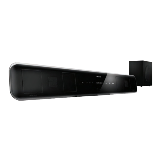
Home Theater System
Contents
1 Technical Specification and Connection Facilities
................................................ 1-1 to 1-2
2 Importand Safety Precautions ......................... 2-1 to 2-2
3 Safety Check After Servicing ..................................... 3-1
4 Safety Information Genard Notes & Lead Free
Requirement ....................................... 4-1
5 Standard Notes For Servicing ................................... 5-1
Pack-IC.................................... 6-1 to 6-3
7 Direction of USE ............................................. 7-1 to 7-5
8 Cabinet Disassembly Instructions ................... 8-1 to 8-3
9 Troubleshooting ......................................................... 9-1
10 Software Upgrading Procedure ............................. 10-1
11 Software Version Check Procedure ...................... 10-2
12 Block Diagram ....................................................... 11-1
13 Wiring Diagram ..................................................... 12-1
14 Main Unit--Touch Board Diagram
Circuit Diagram ............................................13-1
Layout Diagram ...........................................13-1
15 Main Unit--VFD Display Board Diagram
Circuit Diagram ............................................14-1
© Copyright 2010 Philips Consumer Electronics B.V. Eindhoven, The Netherlands.
All rights reserved. No part of this publication may be reproduced, stored in a
retrieval system or transmitted, in any form or by any means, electronic,
mechanical, photocopying, or otherwise without the prior permission of Philips.
Published by KC-LQ 1004 AVM
Version 1.0
Contents
Page
16 Main Unit--Decoder Board Diagram
17 Main Unit--Radio Transmit Board Diagram
18 Subwoofer--Radio Receiver Board Diagram
19 Subwoofer--Power Board Diagram
20 Main Unit Exploded View ...................................... 19-1
21 Subwoofer Exploded View .................................... 19-2
22 Revision List .......................................................... 20-1
Printed in he Netherlands
HTS5110/12/51/98
PT6311 IC Specification ..............................14-2
Layout Diagram ...........................................14-3
Circuit Diagram ...............................15-1 to 15-3
M12L64164A IC Specification ....................15-4
EN29LV320A IC Specification ....................15-5
Circuit Diagram ...............................15-6 to 15-9
UDA1355H IC Specification .....................15-10
Layout Diagram ........................................15-11
Circuit Diagram ................................16-1 to 16-3
Layout Diagram ...........................................16-4
Circuit Diagram ................................17-1 to 17-3
Layout Diagram ...........................................17-4
Circuit Diagram ................................18-1 to 18-2
Layout Diagram ...........................................18-3
Feature
Different /12 /51 /98
Features
RDS
Voltage Selector
ECO Standby
DTS
Subject to modification
Page
EN 3139 785 35230
Advertisement
Table of Contents

Related Manuals for Philips HTS5110


Summary of Contents for Philips HTS5110
-
Page 1: Table Of Contents
Feature Circuit Diagram ..........14-1 Different /12 /51 /98 Features © Copyright 2010 Philips Consumer Electronics B.V. Eindhoven, The Netherlands. Voltage Selector All rights reserved. No part of this publication may be reproduced, stored in a ECO Standby retrieval system or transmitted, in any form or by any means, electronic, mechanical, photocopying, or otherwise without the prior permission of Philips. - Page 2 Technical Specifications and Connection Facilities Technical Specifications and Connection Facilities PCB Locations Main Unit Touch Board-2 Decoder Board Touch Board-1 USB Board Radio Transmit Board VFD Display Board Power Board Radio Receiver Board Subwoofer Power Control Switch 110/220V (for 55/98version) General: Analog Inputs/Outputs 1.4.1...
- Page 3 Technical Specifications and Connection Facilities Video Performance (AUDIO OUT) Coaxial Digital LPCM : according IEC 60958 1.7.1 MPEG 1, MPEG 2, AC3 : according IEC 61937 : according IEC 61937 + addendum CVBS 1.5.1 ≥ 55 dB Lumincance: ≥ 55 dB Y: ≥...
-
Page 4: Importand Safety Precautions
Do not insert warped or cracked discs the combined weight of the product into the disc compartment. • and the wall mount. Koninklijke Philips Remove discs from the disc compartment if you are not using the product for an Electronics N.V. bears no responsibility extended period of time. - Page 5 Important Safety Precautions Disposal of your old product and batteries Your product is designed and manufactured with high quality materials and components, which can be recycled and reused. When this crossed-out wheeled bin symbol is attached to a product it means that the product is covered by the European Directive 2002/96/EC.
-
Page 6: Safety Check After Servicing
Safety Check after Servicing Examine the area surrounding the repaired location for damage or deterioration. Observe that screws, parts, and wires have been returned to their original positions. Afterwards, do the following tests and confirm the specified values to verify compliance with safety standards. 1. -
Page 7: Safety Instructions
Safety Information, General Notes & Lead Free Requirements Safety Instructions Warnings General Safety General Safety regulations require that during a repair: • All ICs and many other semiconductors are susceptible to • Connect the unit to the mains via an isolation transformer. electrostatic discharges (ESD, ). -
Page 8: Standard Notes For Servicing
Due to lead-free technology some rules have to be respected by the workshop during a repair: Pin 1 • Use only lead-free solder alloy Philips SAC305 with order code 0622 149 00106. If lead-free solder- paste is required, please contact the manufacturer Instructions for Connectors of your solder-equipment. -
Page 9: Special Information Of Bga Ic & Flat
2004), containing leaded solder-alloy and components, all needed spare-parts will be available till the end of the service-period. For repair of such sets nothing changes. • On our website www.atyourservice.ce.Philips.com you find more information to: Fig. S-1-1 • BGA-de-/soldering (+ baking instructions) 2. - Page 10 3. The flat pack-IC on the CBA is affixed with glue, so With Iron Wire: be careful not to break or damage the foil of each 1. Using desoldering braid, remove the solder from pin or the solder lands under the IC when all pins of the flat pack-IC.
- Page 11 Special Information BGA IC & Flat Pack-IC Instructions for Handling Semi- 2. Installation conductors 1. Using desoldering braid, remove the solder from the foil of each pin of the flat pack-IC on the CBA Electrostatic breakdown of the semi-conductors may so you can install a replacement flat pack-IC more occur due to a potential difference caused by easily.
-
Page 12: Direction Of Use
Direction of Use The following excerpt of the DFU/QSG serves as an introduction to the set. The Complete Direction for Use can be download in different languages from the internet site of Philips Customer care Center: www.p4c.philips.com Remote Control •... - Page 13 Direction of Use Remote Control Marks two points within a chapter or track for repeat play, or turns off repeat mode. REPEAT / PROGRAM • Selects a repeat or shuffle mode. • In radio mode, programs radio stations. SUBTITLE Selects a subtitle language for video. SURROUND Selects Dolby Virtual Speaker surround sound.
-
Page 14: Home Theater
TV and other devices. The basic connections of the home theater with its accessories are provided in the Quick Start. For a comprehensive interactive guide, see www. DC IN connectivityguide.philips.com. Connects to the AC-DC adapter. Note VIDEO OUT (CVBS) Connects to the composite video input •... - Page 15 If the TV supports EasyLink HDMI CEC, the TV or other devices such as a cable box. control the home theater and TV with one remote control (see ‘Use Philips EasyLink’ on Choose from the following connectors. page 17). Option 1: Connect audio through a...
- Page 16 Direction of Use Option 2: Connect audio through analog audio cables Option 3: Connect audio through an HDMI cable Note • The HDMI connector on the TV might be labeled HDMI 1 or HDMI ARC. This feature works with Audio Return Channel (ARC) compatible devices only.
-
Page 17: Cabinet Disassembly Instructions
Cabinet Disassembly Instructions 1. Disassembly Flowchart This flowchart indicates the disassembly steps to gain Note: access to item(s) to be serviced. When reassembling, (1) Identification (location) No. of parts in the figures follow the steps in reverse order. Bend, route, and (2) Name of the part dress the cables as they were originally. - Page 18 Cabinet Disassembly Instructions [3]A05 Decoder Board [2]A06 CON7 CON6 [3]A05 Fig. D2 [4] A06 CN201 CN200 CN203 Display Board CN202 TX-Board [5] A07 Fig. D3...
- Page 19 Cabinet Disassembly Instructions [6] A09 [6] A09 Touch-Board CN101 CN102 Touch-Board Fig. D4 [7] A08 Tweeter Mediant Speaker [7] A08 [7] A08 Fig. D5...
-
Page 20: Troubleshooting
Troubleshooting FLOW CHART NO.1 The power cannot be turned on. Check the Power Switching Adaptor if it has DC 27V output . Try to replace a new Power Switching Adaptor Check the 1st pin of IC1501 which location is U1 Replace the L2 &... -
Page 21: Software Upgrading Procedure
Software Upgrading Procedure 1, Download the Software from Philips support Website: http://www.philips.com/support. 2, Copy the Software upgrade file into USB Device. C, Press the “OK” on the Remote Control. A, Connect to TV and Turn on Main Unit Main unit Screen Display:... -
Page 22: Software Version Check Procedure
Software Version Check 1, Select the “Menu”, like below show: Press OK on Remote Control: 2, TV Screen Display: 2, Select to get the Version information : 10-2... -
Page 23: Block Diagram
Block Diagram DC1.8V DC3 3V CVBS CVBS SDRAM DC5V DC1.8V M12L64164A-7T CX1117 DC1.8V DC IN FLASH 2M * 8 bits AP1501-5V AC IN DC OUT SWITCHING MX29LV160 POWER Main chipset DC3.3V SUPPLY SERIAL EEPROM DC_5V 24C02 HDMI CX1117 DC3.3V Switching Power Adaptor APM9435M HDMI_ARC MPEG_ON... -
Page 24: Wiring Diagram
Wiring Diagram Cable Location Touch Board-1 NO.:5 CN101 CN102 Cable Location NO.:6 Touch Board-2 CN202 CN203 CN200 CN201 CN901 CN901 CN902 CN902 VFD Display Board Frequency Frequency Divider Board Divider Board CON7 CON9 CN400 CN401 CON3 AUX L AUX R MP3_IN_L USB Board MP3_IN_R... -
Page 25: Layout Diagram
Main Unit--Touch Board Circuit & Layout Diagram Touch Board-1 3.3V CN102 KEY4 DGND KEY5 LED103 KEY6 LED105 3.3V LED104 Touch Board-2 3.3V CN101 3.3V LED106 KEY1 LED101 KEY2 LED102 KEY3 LED107 DGND 13-1 13-1... - Page 26 Main Unit--VFD Display Board Circuit Diagram 3.3V VOL+ KEY1 (POWER) U201 POWER KEY2 OUT0 (VOL-) VFD201 SI[0] OUT1 R208 SI[1] OUT3 VOL- KEY3 SI[3] (SOURROUND) HL-D1068W SI[8] SI[10] OUT8 R209 SOURROUND KEY4 SI[11] OUT10 (SOUND MODE) OUT11 SOUND MODE KEY5 (SOURCE) IC-WT5700-S160 KEY6...
-
Page 27: Pt6311 Ic Specification
PT6311 IC Specification • 87% Efficiency Switching Regulator (ISR) designed to • Adjustable Output Voltage meet the on-board power conversion • Internal Short Circuit Protection needs of battery powered or other equip- • Over-T emperature Protection ment requiring high efficiency and •... -
Page 28: Layout Diagram
Main Unit--VFD Display Board Layout Diagram TOP Layout Diagram Bottom Layout Diagram 14-3 14-3... - Page 29 Main Unit--Decoder Board Circuit Diagram Power support MPEG_ON MPEG_ON 27V_IN DC5V AP1501-5V 47uH_3A FB/1206 APM9435K VOUT FB/1206 0.1uF CD11X/220UF16V/D6.3H7 0.1uF CD11/100UF35V/D8H14 CD263/470UF16V/D8H12 0.1uF 0.1uF CD11X/220UF16V/D6.3H7 SK34 CD11/47UF35V/D8H14 0.1uF/0603 MPEG_ON 2N3904 0.1uF 4750mA 27V_IN DVD3.3V 89S_3V3 CD263/100UF35V/D8H7 DC-005 27V_IN 0.1uF CD11X/220UF16V/D6.3H7 0.1uF HOLE/GND DVD3.3V...
- Page 30 Main Unit--Decoder Board Circuit Diagram TX0+ TX0+ TX0- TX0- TX1+ TX1+ TX1- TX1- TX2+ TX2+ ADACVDD 150uH/DIP 89S 3V3 TX2- 89S 3V3 TX2- APLLVDD3 47uH/DIP TXC+ TXC+ JITFO JITFN DACVDD3 1000pF TXC- TXC- 750K CB20 + CE17 CB21 CB22 CB24 + CE18 TS DATA2 CB25...
- Page 31 Main Unit--Decoder Board Circuit Diagram SDRAM & FLASH DQ[0..15] DQ[0..15] MA[0..11] MA[0..11] BA[0..1] BA[0..1] DQM[0..1] DQM[0..1] 2 DCLK DCLK DCKE DCKE 33x4 CAS# CAS# DCS# RAS# RAS# DRAS# RAS# DCAS# CAS# DWE# MA10 DQ10 A10/AP DQ10 DBA0 MA11 DQ11 DQ11 DBA0 DQ12 PCE#...
-
Page 32: M12L64164A Ic Specification
M12L64164A IC Specification SDRAM 1M x 16 Bit x 4 Banks FUNCTIONAL BLOCK DIAGRAM Synchronous DRAM Clock Generator Bank D Bank C Bank B FEATURES Address Address ORDERING INFORMATION Buffer JEDEC standard 3.3V power supply Bank A Mode & LVTTL compatible with multiplexed address Register Refresh 54 Pin TSOP (Type II) -
Page 33: En29Lv320A Ic Specification
EN29LV320A IC Specification PRODUCT SELECTOR GUIDE 32M FLASH USER MODE TABLE DQ8-DQ15 Speed Option RESET WP#/AC DQ0- BYTE# BYTE# Operation Max Access Time, ns (t Read DQ8- Max CE# Access, ns (t DQ14= Write (Note 1) High-Z, Max OE# Access, ns (t Accelerated DQ15 = Program... - Page 34 Main Unit--Decoder Board Circuit Diagram Decoder Board Video Out CVBS CVBS CVBS_OUT CVBS_OUT +5VV FB/0603 CE32 CB75 CD11X/22UF16V/D4H7 0.1uF +5VV CB74 CD11X/100UF16V/D6.3H7 0.1uF 1.8uH/0603 3.3K CE31 CD11X/220UF16V/D6.3H7 CVBS CE102 2N3904 CVBS_OUT 160 1% 47pF 47pF 2.2K 75 1% PESD12VS2UT 15-6 15-6...
- Page 35 Main Unit--Decoder Board Circuit Diagram HDMI Circuit Diagram TXC+ TXC+ TXC- TXC- TX2+ TX0+ TX0+ TX0- TX0- TX2- TX1+ TX1+ TX1- TX1- TX2+ TX2+ TX2- TX2- TX1+ TS_DATA2 TS_DATA2 CECOUT R106 TX1- HDMI_SCL GPIO[5..7] GPIO[5..7] 2 HDMI_SDA CECOUT CECOUT CB135 1000pF DV33 TX0+...
- Page 36 Main Unit--Decoder Board Circuit Diagram AUDIO & FM FB/0603 R114 R115 DC5V R116 CD11X/100UF16V/D5H7 R120 AUX IN R AUX INR MP3 IN L MP3 INL CE37 CES2307 0 1uF R117 R118 R119 R113 R120 CE36 470pF 470pF R122 0 1uF R123 SI4702/03 CD11X/220UF16V/D6 3H7...
- Page 37 Main Unit--Decoder Board Circuit Diagram R209 R210 NC/100K VADC3 3V R211 R212 NC/100K CB95 27V FAN/2313 R377 10K CE103 1N4148 FB/1K 0 1uF/0402 R237 LOUT+ VDAC3 3V R214 4 7K 330R/1W SWOUT R CB96 4 7uF/10 R215 4 7K SWOUT L 0 1uF R395 CE104...
-
Page 38: Uda1355H Ic Specification
UDA1355H IC Specification PINNING SYMBOL DESCRIPTION BCKI bpt4mtht5v bit clock input (master or slave) bpt4mtht5v word select input (master or slave) DATAI iptht5v digital data input BLOCK DIAGRAM LOCK op4mc PLL lock indicator output SPDIFOUT op4mc SPDIF output vdde digital pad supply voltage vsse digital pad ground DATAO... -
Page 39: Layout Diagram
Main Unit--Decoder Board Layout Diagram Bottom Layout Diagram TOP Layout Diagram 15-11 15-11... - Page 40 Main Unit--Radio Transmit Board Circuit Diagram RF_CE_RX RF_CE_RX FIDC RF_CS_TX RF_CE_TX RF_DIO RF_DIO RF_DCLK RF_DCLK RF_DCLK P1_0 RF_PEN RF_PEN RF_PEN P1_1 RF_SCLK RF_SCLK RF_SCLK SM_1 3.3V RF_SI RF_SI RF_SI SM_0 RF_SO RF_SO RF_SO VSS25 HMX6026E1 HMX6026E1 AUDIOL-IN TP16 TP16 +2.5V VSS33 VDD25 AUDIOR-IN...
- Page 41 Main Unit--Radio Transmit Board Circuit Diagram TP14 TP14 CE2632 CE2632 100uF 100uF R-IN R-IN AUDIOR-IN DVDD33 R-IN 0.1uF 0.1uF L-IN L-IN 6800pF 6800pF DGND AVDD33 L-IN 100uF 100uF CODEC_TX DOUT 0.1uF 0.1uF TP15 TP15 SCLK AGND AUDIOL-IN 6800pF 6800pF LRCLK LRCK MCLK 10uF...
- Page 42 Main Unit--Radio Transmit Board Circuit Diagram +1.8V CLK_16M 68pF 68pF 68pF 68pF +1.8V TP-ANT TP-ANT 3.3V +1.8V 0.1uF 0.1uF 0.1uF 0.1uF DVDD3.3 DVDD1.8 +1.8V RF_CE_RX AVDD_SW RF_CE_RX 5.6pF 5.6pF RF_CS_TX RF_CE_TX RF_DIO RF_N DIO/PKT RF_DIO 4.7nH 4.7nH CC2400 2 L3 33nH 33nH RF_DCLK...
-
Page 43: Layout Diagram
Main Unit--Radio Transmit Board Layout Diagram TOP Layout Bottom Layout 6026TXD 6026RXD DODEC-CE TP16 FIDC RESET AUDIO-L AUDIO-R V3.3 16-4 16-4... - Page 44 Subwoofer--Radio Receiver Board Circuit Diagram +1.8V CLK_16M 68pF 68pF 68pF 68pF +1.8V 3.3V +1.8V 145106 145106 TP-ANT TP-ANT 0.1uF 0.1uF 0.1uF 0.1uF DVDD3.3 DVDD1.8 +1.8V RF_CE_RX AVDD_SW RF_CE_RX 5.6pF 5.6pF RF_CS_TX RF_CE_TX RF_DIO RF_N DIO/PKT RF_DIO CC2400 4.7nH 4.7nH 2 L3 22nH 22nH RF_DCLK...
- Page 45 Subwoofer--Radio Receiver Board Circuit Diagram 47uF 47uF CODEC_RX SCLK BCLK LRCLK LRCK 47uF 47uF MCLK MCLK CE2711 CE2711 Q4 MMBT3904 Q4 MMBT3904 0.01uF 0.01uF 0.01uF 0.01uF 12 HEADER 12 HEADER 100uF 100uF MUTE_N STATE1 10uH 10uH MUTE STATE3 STATE2 CTRL 20pF 20pF 20pF...
- Page 46 Subwoofer--Radio Receiver Board Circuit Diagram 3.3V V4.0--2K LED1 LED1 330E 330E RF_CE_RX 蓝色 RF_CE_RX FIDC RF CS TX RF_CE_TX RF_DIO RF_DIO RF Connector LED-2 LED-2 RF DCLK STATE1 STATE1 RF_DCLK RF_DCLK P1_0 RF PEN RF_PEN RF_PEN P1_1 STATE2 3.3V +2.5V RF_SCLK EM78P153SN EM78P153SN...
-
Page 47: Layout Diagram
Subwoofer--Radio Receiver Board Layout Diagram TOP Layout Diagram Bottom Layout Diagram 17-4 17-4... - Page 48 Subwoofer--Power Board Circuit Diagram PQ32/30 Lp=0.49mH DR6*15 3uH 16A/200V MOV1 471M/400V MF72 8D13 47K/2W 10mH T18*10*10 220uF/200V UU16-30mH 2200uF/35V R28,29,27 104/100V 222/1KV 1000uF/35V 4*IN5408 3x100R/1206 3A/1KV 0.22uF/275V MOV2 2x1M1206 0.22uF/275V 103/600V 10K/1206 220uF/200V 471M/400V DR6*15 3uH 16A/200V CE10 100V/ON 115/230Vac CON4 240V/OFF 104/100V...
- Page 49 Subwoofer--Power Board Circuit Diagram +23V 3uH/6A CE12 CE15 104/50V 102/50V 1000uF/35V T12x6x4(8uH) 220uF/35V 5.6K/0805 474/50V 105/50V 102/50V 0R/0805 CE21 47K/0805 T12x6x4(8uH) 5.6K/0805 474/50V CE13 220uF/35V 102/50V 47K/0805 334/50V 3uH/6A 102/50V 2.2K/1/6W 1000uF/35V 104/50V 5.6K/0805 5.6K/0805 2N5401 -23V CE22 8050 474/50V 220uF/35V 4.7K/0805 104/50V...
- Page 50 Subwoofer--Power Board Layout Diagram Bottom Layout Diagram TOP Layout Diagram 18-3 18-3...
-
Page 51: Main Unit Exploded View
Main Unit Exploded View Location no. Screw Specification D3.5 x 12 BA D4 x 30 BA D3 x 10 FA D2 x 6 FA D3 x 10 PA D3 x 8 PA D3 x 6 PT D3 x 8 BA D2 x 4 PWB 19-1 19-1... -
Page 52: Subwoofer Exploded View
Subwoofer Exploded View Location no. Screw Specification D3 x 12 BAH D3 x 16 BAH D3.5 x 16 BAH D3 x 6 BM M3 NUT D2 x 5 PT 19-2 19-2... -
Page 53: Revision List
Revision List Revision List Version 1.0 * Initial Release 20-1...
Need help?
Do you have a question about the HTS5110 and is the answer not in the manual?
Questions and answers