Philips HTS5120/12 Service Manual
Hide thumbs
Also See for HTS5120/12:
- Quick start manual (12 pages) ,
- User manual (25 pages) ,
- Quick start manual (12 pages)
Table of Contents
Advertisement
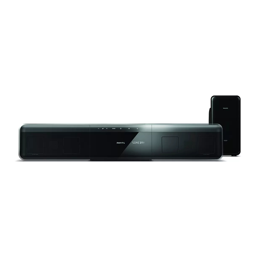
Home Theater System
CLASS 1
LASER PRODUCT
Contents
1 Repair Scenario Matrix ...............................................1-1
3 Laser Beam Safety Precautions..................................3-1
4 Important Safety Precautions ......................... 4-1 to 4-2
5 Safety Check After Servicing .................................... 5-1
Requirement ............................ 6-1 to 6-2
7 Standard Notes For Servicing .................................. .7-1
................................................... 8-1 to 8-3
9 Direction of Use ...............................................9-1 to 9-5
10 Cabinet Disassembly Instructions ................... 10-1 to 10-2
11 Troubleshooting ..................................................... 11-1
12 Software Upgrading Procedure ............................. 12-1
13 Software Version Check ........................................ 12-2
14 Block Diagram ........................................................13-1
15 Wiring Diagram ...................................................... 14-1
Circuit Diagram ................................. 15-1
Layout Diagram ................................ 15-1
WT5700 IC Specification ................. 15-2
17 Main Unit--VFD Display Board
Circuit Diagram ................................. 15-3
PT6311 IC Specification ................... 15-4
Layout Diagram ................................ 15-5
Circuit Diagram ................................. 15-6
Layout Diagram ................................ 15-6
© Copyright 2010 Philips Consumer Electronics B.V. Eindhoven, The Netherlands.
All rights reserved. No part of this publication may be reproduced, stored in a
retrieval system or transmitted, in any form or by any means, electronic,
mechanical, photocopying, or otherwise without the prior permission of Philips.
Published by KC-KM 1030 AVM
Version 1.1
Page
Contents
19 Main Unit--Decoder Board Circuit Diagram
24 Main Unit Exploded View ............................................ 16-1
25 Subwoofer Exploded View ...........................................16-2
26 Packing Exploded View ...............................................16-3
27 Revision List ................................................................17-1
Printed in he Netherlands
HTS5120/12/51/55/78/93/98
Circuit Diagram ...................... 15-7 to 15-10
Circuit Diagram ...................... 15-12 to 15-15
Layout Diagram ................................ 15-17
Circuit Diagram .................................. 15-18
Layout Diagram ................................. 15-19
Circuit Diagram ...................... 15-20 to 15-22
CC2400 IC Specification .................. 15-23
Layout Diagram ................................. 15-24
Circuit Diagram ..................... 15-25 to 15-27
Layout Diagram ................................. 15-28
Circuit Diagram ..................... 15-29 to 15-30
TDA8920 IC Specification ................ 15-31
Layout Diagram ................................. 15-32
Feature
Different /12 /51 /55 /78 /93 /98
Features
RDS
Voltage Selector
ECO Standby
DTS
Subject to modification
Page
EN 3139 785 35241
Advertisement
Table of Contents


Need help?
Do you have a question about the HTS5120/12 and is the answer not in the manual?
Questions and answers