NAD T747 Service Manual
Hide thumbs
Also See for T747:
- Owner's manual (42 pages) ,
- Specifications (3 pages) ,
- Owner's manual (43 pages)
Table of Contents
Advertisement
Advertisement
Chapters
Table of Contents

Related Manuals for NAD T747


Summary of Contents for NAD T747
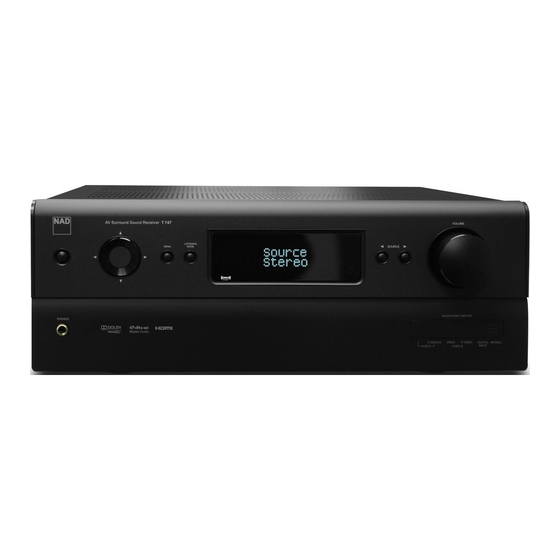
- Page 1 T747 AV Surround Sound Receiver...
-
Page 2: Table Of Contents
SECTION 1 SUMMARY CONTENTS PRODUCT SAFETY SERVICING GUIDELINES..................1-3 SERVICING PRECAUTIONS ........................1-4 * General Servicing Precautions * Insulation checking prodedure * Electrostatically Sensitive Devices SPECIFICATIONS ............................1-5 DISASSEMBLY .............................. 1-6 PRINCIPAL PART LOCATION ........................1-7 EXPLODED VIEW ............................1-8... -
Page 3: Product Safety Servicing Guidelines
PRODUCT SAFETY SERVICING GUIDELINES CAUTION : DO NOT ATTEMPT TO MODIFY THIS PRODUCT IN VOLTAGE MEASURE MUST NOT EXCEED 75 VOLTS R.M.S. ANY WAY. NEVER PERFORM CUSTOMIZED INSTALLATIONS THIS CORRESPONDS TO 0.5 MILLIAMP AC ANY VALUE WITHOUT MANUFACTURER’S APPROVAL. UNAUTHORIZED EXCEEDING THIS LIMIT CONSTITUTES A POTENTIAL MODIFICATIONS WILL NOT ONLY VOID THE WARRANTY, BUT SHOCK HAZARD AND MUST BE CORRECTED IMMEDIATELY. -
Page 4: Servicing Precautions
SERVICING PRECAUTIONS CAUTION : Before servicing the A/V Receiver covered by this Electrostatically Sensitive (ES) Devices service data and its supplements and addends, read and follow the Some semiconductor (solid state) devices can be damaged easily by SAFETY PRECAUTIONS. NOTE : if unforeseen circumstances static electricity. -
Page 5: Specifications
SPECIFICATIONS... -
Page 6: Disassembly
DISASSEMBLY 1> REMOVAL OF TOP COVER 2> REMOVAL OF FRONT PANEL... -
Page 7: Principal Part Location
PRINCIPAL PARTS LOCATION... - Page 8 T747AH EXPLODED VIEW PARTS LIST (Graphite) BUTTON NOTE ** AMP ASSEMBLY #31 & CHASSIS #19 ARE SOLD TOGETHER FASCIA ASSEMBLY #1, #3, & #4 ARE SOLD TOGETHER...
- Page 9 T747AH EXPLODED VIEW (Graphite) NOTE** NOTE** NOTE** 1-10...
- Page 10 T747C EXPLODED VIEW PARTS LIST (Graphite) BUTTON NOTE ** AMP ASSEMBLY #31 & CHASSIS #19 ARE SOLD TOGETHER FASCIA ASSEMBLY #1, #3, & #4 ARE SOLD TOGETHER 1-11...
- Page 11 T747C EXPLODED VIEW (Graphite) NOTE** NOTE** NOTE** 1-12 1-13...
- Page 12 T747CT EXPLODED VIEW PARTS LIST (Titanium) BUTTON NOTE ** AMP ASSEMBLY #31 & CHASSIS #19 ARE SOLD TOGETHER FASCIA ASSEMBLY #1, #3, & #4 ARE SOLD TOGETHER 1-14...
- Page 13 T747CT EXPLODED VIEW (Titanium) NOTE** NOTE** NOTE** 1-15 1-16...
- Page 14 SECTION 2 ELECTRICAL CONTENTS CONTENTS IC BLOCK DIAGRAMS & PIN DESCRIPTION ..................2-2 DIAGRAM..............................2-31 1. BLOCK DIAGRAM ..........................2-31 2. WIRING DIAGRAM ..........................2-39 3. SCHEMATIC DIAGRAM ........................2-41 • FRONT PART ..........................2-41 • POWER PART..........................2-43 • MCU PART..........................
-
Page 15: Ic Block Diagrams & Pin Description
IC BLOCK DIAGRAMS & PIN DESCRIPTION... - Page 17 IC201: T5CC1: Microcontrollers...
- Page 18 IC PIN DESCRIPTION (IC158: ADV7342: VIDEO ENCODER) 64 63 62 61 60 59 58 57 56 55 54 53 52 51 50 49 SFL/MISO DD_IO PIN 1 TEST0 SET1 TEST1 COMP1 DAC 1 DAC 2 ADV7342/ADV7343 DAC 3 TOP VIEW (Not to Scale) AGND DAC 4...
- Page 19 Input/ Pin No. Mnemonic Output Description This pin is used to control the amplitudes of the DAC 4, DAC 5, and DAC 6 outputs. A 4.12 kΩ SET2 resistor must be connected from R to AGND. SET2 45, 35 COMP1, Compensation Pins.
- Page 20 IC240: CS497004: DSP GPIO9, PCP_A1 / A9 SD_A0, EXT_A0 SD_A1, EXT_A1 GPIO8, PCP_A0 / A8 SD_A2, EXT_A2 GPIO7, PCP_AD7 / D7 GND4 GPIO6, PCP_AD6 / D6 SD_A3, EXT_A3 VDDIO7 SD_A4, EXT_A4 GPIO5, PCP_AD5 / D5 VDD4 GPIO4, PCP_AD4 / D4 EXT_CS2# GNDIO7 SD_A5, EXT_A5...
- Page 21 IC PIN DESCRIPTION (IC153: A3S56D40ETP: DDR RAM) DQ15 VDDQ VDDQ VSSQ VSSQ DQ14 DQ13 VSSQ VSSQ VDDQ VDDQ 66pin TSOP(II) DQ12 DQ11 VDDQ VDDQ VSSQ VSSQ DQ10 VSSQ VSSQ VDDQ VDDQ 400mil width VDDQ VDDQ VSSQ VSSQ 875mil length UDQS LDQS VREF VREF...
- Page 22 SYMBOL TYPE DESCRIPTION Clock: CLK and /CLK are differential clock inputs. All address and control input signals are sampled on the crossing of the positive edge of CLK and CLK, /CLK Input negative edge of /CLK. Output (read) data is referenced to the crossings of CLK and /CLK (both directions of crossing).
-
Page 23: Diagram
BLOCK DIAGRAM DQ0 - 7 BLOCK DIAGRAM A3S56D30ETP I/O Buffer DQS Buffer Memory Memory Memory Memory Array Array Array Array Bank #0 Bank #1 Bank #2 Bank #3 Mode Register Control Circuitry Address Buffer Control Signal Buffer Clock Buffer /CS /RAS /CAS /WE A0-12 BA0,1 /CLK... - Page 24 BLOCK DIAGRAM (IC152: ES29LV320FT70TG) 2-11...
- Page 25 BLOCK DIAGRAM (IC151: FLI30336AC) 2-12...
- Page 26 BLOCK DIAGRAM (IC134: NJM2285) 2-13...
- Page 27 IC113: NJM2566V: VIDEO AMP) 2-14...
- Page 28 BLOCK DIAGRAM (IC133: NJM2581) VIN1 75 Ω Driver BIAS VEE1 VOUT1 VIN2 75 Ω Driver BIAS VEE2 VOUT2 VIN3 75 Ω Driver BIAS VEE3 VOUT3 PowerSave BLOCK DIAGRAM (IC135: NJM2586A) CH1 OUT CH1 IN1 Driver Bias Cont1 CH1 OUT CH1 IN1 Driver Cont1 Bias...
- Page 29 IC131: NJW1321FP: VIDEO SW) 2-16...
- Page 30 2-17...
- Page 31 IC301: R2A15218FP: 8CH ELECTRONIC VOLUME SYSTEM BLOCK DIAGRAM Multi Multi SUBL Rch Tone Lch Tone MUTE CLOCK DATA MCU I/F DGND Lout Tone Volume Bass& Treble Volume Bass& Treble Rout Input Volume Volume Multi SBLout Out L SBLin Volume Volume Multi SBRout SBRin...
- Page 32 BLOCK DIAGRAM AND PIN CONFIGURATION (TOP VIEW) AVCC MUTE AVCC N.C. AVEE AVEE N.C. TREL 0/-6/-12/-18dB ADCL BASSL2 ADCR BASSL1 N.C. AGND Bass/ Treble 0~-95dB, -14~+14dB +42~0dB MAIN N.C. (2dB step) (0.5dBstep) (0.5dBstep) Bypass Tone INR1 Tone+MIX FROUT Tone INL1 AGND +42~0dB (0.5dBstep)
- Page 33 PIN DESCRIPTION PIN No. Function Name 23,21, FROUT,FLOUT, 17,15, COUT,SWOUT, Output pin of FL/FR/C/SW/SL/SR/SBL/SBR channel 11,9, SROUT, SLOUT, SBROUT,SBLOUT 24,20, FRC,FLC, 18,14, CC,SWC, Connects capacitor for reducing click noise of 12,8, SRC,SLC, L/R/C/SW/SL/SR/SBL/SBR channel volume SBRC,SBLC 4,7,10,16, Analog ground of internal circuit AGND 19,22,56 TREL, TRER...
- Page 34 IC173: SII9134CUT: HDMI TRANSMITTER CVCC18 CI2CA CSDA CSCL DSDA DSCL DDCPWR5V AVCC33 AGND PVCC2 AGND IC173 TX2+ TX2- SII9134CTU IDCK AVCC18 IOVCC33 TX+1 TX1- AGND TX0+ TX0- AVCC18 TXC+ TXC- AGND PVCC1 CVCC18 EXT_SWG AGND 2-21...
-
Page 35: Block Diagram
BLOCK DIAGRAM 2-22... - Page 36 IC146: SII9135CTU: HDIM RECEIVER AVCC18 AVCC33 CVCC18 R0XC- CGND R0XC+ AGND AVCC33 R0X0- R0X0+ IOVCC33 AGND IOGND AVCC33 R0X1- R0X1+ AGND AVCC33 CVCC18 R0X2- CGND R0X2+ IC146 AGND AVCC18 SII9135CTU RSVDNC AVCC33 IOVCC33 R1XC- IOGND R1XC+ AGND AVCC33 R1X0- R1X0+ CVCC18 AGND CGND...
- Page 37 BLOCK DIAGRAM 2-24...
- Page 38 IC141: SII9185ACTU: HDMI SWITCH R1X0- AGND R1X0+ R0XC+ AVCC33 R0XC- R1X1- AVCC18 R1X1+ HPD0 AGND LSCL R1X2- LSDA R1X2+ RESET# 9185ACTU AVCC18 EXTSWING DSDA1 TXC- DSCL1 TXC+ RPWR1 AGND CEC_D TX0- CEC_A TX0+ AVCC33 AVCC18 HPD2 TX1- AVCC18 TX1+ R2XC- AGND TX2- R2XC+...
- Page 39 BLOCK DIAGRAM 2-26...
- Page 40 IC157: ST232CDR: RS-232 DRIVERS & RECEIVERS PlN N° SYMBOL NOTE Positive terminal for the first charge pump capacitor Doubled voltage terminal Negative terminal for the first charge pump capacitor Positive terminal for the second charge pump capacitor Negative terminal for the second charge pump capacitor Inverted voltage terminal Second transmitter output voltage Second receiver input voltage...
- Page 41 IC147: TC74VCX541FT: OCTAL BUS BUFFER 2-28...
- Page 42 IC156: M24C32WMN6TP: EEPROM High Voltage Control Logic Generator I/O Shift Register Address Register Data and Counter Register 1 Page X Decoder AI06899 2-29...
- Page 43 TRANSISTOR, REGULATOR IC BLOCK DIAGRAM 2-30...
- Page 44 BLOCK DIAGRAM (AUDIO PART) 2-31 2-32...
- Page 45 BLOCK DIAGRAM (MCU & DSP PART) 2-33 2-34...
- Page 46 BLOCK DIAGRAM (HDMI PART) 2-35 2-36...
- Page 47 BLOCK DIAGRAM (VIDEO PART) 2-37 2-38...
-
Page 48: Wiring Diagram
WIRING DIAGRAM POWER CORD POWER (MCU) FAN-->AMP #3(VIDEO) 1.25 1.25 AMP-->POWER 450mm 70mm 300mm 450mm INPUT-->VIDEO POWER-->INPUT 350mm #2(INPUT) #4(HDMI) 1.25 1.25 AMP-->CONNECT TRANSFORMER #1(AMP) 1.25 HEATSINK #1 FAN #2 FAN 300mm 1.25 H/P-->CONNECT 180mm 50mm 2.0 pitch FRONT 3-39 3-40... -
Page 49: Schematic Diagram
SCHEMATIC DIAGRAM (FRONT PART) TO POWER TRANS. CN502 VFD PCB CUP12126-1 PHONES & OPTICAL PCB CUP12126-4 JK522 D+5V D+5V R5009 FIP51 CFLHCA16S201T BN507 & CN507 OPT_IN OPT_IN DGND DGND 56 55 MIC_IN MIC_IN R5056 MIC_ON MIC_ON IC522 HVITC74VHCT08FT R5045 R5204 1(1/4) Q5051 C2316Y... -
Page 50: Power Part
SCHEMATIC DIAGRAM (POWER PART) -12V DAB+8V CUP12126-3 +12V DETECT D5310 D5312 STBY_MUTE R5708 IC537 R5305 D5305 1N4003 1N4003 D5311 D5313 CUP12126-2 0.15 SB2100 STBY_MUTE 1N4003 1N4003 D5304 SB2100 R5315 DETECT +12V D5307 DAB+6.5V 1N4003S -12V D5306 R5304 IN OUT D5710 0.15 1N4003S 1N5819... -
Page 51: Mcu Part
SCHEMATIC DIAGRAM (MCU PART) 3-45 3-46... -
Page 52: Dsp&Codec With Dir Part
SCHEMATIC DIAGRAM (DSP&CODEC WITH DIR PART) 3-47 3-48... -
Page 53: Input&Volume Part
SCHEMATIC DIAGRAM (INPUT&VOLUME PART) XM PART FROM FRONT B'D BN311 JK301 GAIN : 20dB R3003 ANALOG1_L +12V R3321 1W / 68ohm REC OUT1 Q3321 R3323 C3203 ANALOG_OUT R3004 ANALOG1_R R3109 R3110 SW_MUTE2 SBR_OUT C3027 R3001 5.6K 5.6K RECOUT1_L C3104 D3110 FUNC_MUTE2 ANALOG 1 10/50V... -
Page 54: Xm&Tuner Part
SCHEMATIC DIAGRAM (XM&TUNER PART) XM READY PART +5VX GAIN : 6dB / F.RESPONSE : 44kHz @ -3dB RN343 XM_MCLK MCLK DZFL XM_LRLK C3451 R3453 C3453 C3461 XM_BCLK BICK DZFR 10/50V(U) 3.3K(U) 1000P(U) 10/50V(U) R3459 R3455 22X4(U) 3.3K(U) XM_DATA SDTI C3459 2.2K(U) 100P(U) LRCK... -
Page 55: Video Part
SCHEMATIC DIAGRAM (VIDEO PART) MIC_R 470/10V R1306 C1312 MIC_L MONITOR 470/10V R1305 C1311 JK131 CVBS GAME_R 470/10V R1304 C1310 R1334 GAME_L VGND 1/50V VGND VGND VGND 10/50V C1386 C1306 C1305 10/50V IC133 HVINJM2581MTE1 1/50V C1387 CVBS VGND 1/50V 10/50V C1388 C1304 MIC_R R1335... -
Page 56: Hdmi Part
SCHEMATIC DIAGRAM (HDMI #1 PART) HDMI ENCODER PART FLI30336 ANALOG INPUT VIDEO<-->TORINO COMPONENT PR COMPONENT PB COMPONENT Y CVBS DO NOT MOVE. CVBS_IN SV_Y_IN SV_C_IN FS_SELECT V_AGND COMP_Y1 SD(13.5MHZ) MODE : LOW HD(30MHZ) MODE : HIGH COMP_PB1 Control by Torino COMP_PR1 V_AGND +5VV... - Page 57 SCHEMATIC DIAGRAM (HDMI #2 PART) HDMI RX & TX PART HDMI_INTERFACE TORINO<-->ENCODER&TX_RX TORINO<-->RX&TX HVIKIC7SZ08FU IC148 3.3V_HD_ALL HDMI_INPUT<-->TX&RX +3.3V_IO R1459 HDMI_SCL HDMI_SCL 4.7K R1460 DDC+5V HDMI_SDA HDMI_SDA 4.7K V_DGND V_DGND D_DATA R1461 R1462 D_CLK C1436 OPEN IN4_D_DATA R1463 C1435 OPEN IN4_D_CLK R1464 V_DGND 1.8V_HD(SII9134)
- Page 58 SCHEMATIC DIAGRAM (HDMI #3 PART) HDMI SCALER PART +3.3V_IO +1.8V_ADC +3.3V_PLL +3.3V_ADC +1.8V_PLL +2.5V_DDR +1.8V_CORE +3.3V_LVDS +3.3V_LVDS_PLL +3.3V_LBADC V_DGND V_DGND V_DGND V_DGND V_DGND V_DGND TORINO<-->ENCODER&TX_RX V_DGND V_DGND V_DGND V_DGND V_DGND +2.5V_DDR V_DGND V_DGND V_DGND V_DGND V_DGND V_DGND TORINO<-->DDR VIDEO<-->TORINO SV_C_IN R1504 C1520 0.1uF...
- Page 59 SCHEMATIC DIAGRAM (HDMI #4 PART) HDMI SW PART D1401 DDC+5V C1405 IC143 DDC+5V DDC+5V AT24C02N IC142 R1440 TC7MZ4052FK Q1413 KRC103S Q1410 KRA102S Q1412 V_DGND UPA672T Q1411 R1441 V_DGND C103S IN4_D_DATA R1431 V_DGND IN4_D_CLK HP DET V_DGND HDMI_SCL R1433 C1404 R1434 HDMI_SDA 0.1uF R1435...
- Page 60 SL_IN KTA1268GR KTA1268GR R4831 R4832 10/50V R4401 R4405 SR_IN SL_IN 2.7K/1.5K 150/680 R4412 R4827 C4401 VR440 Q4822 3.3K BSL_IN 560K T747 T737 L4426 KTA1268GR Q4412 R4831 2.7K 1.5K KTD1028B 0.5uH BSR_IN R4403 R4832 R4426 SL_CH R4427 R4407 R4826 -12V 2.2K...
- Page 61 Fan1 ON R4992 HEADPHONE ON IPOD_TX DAB_ON R4993 Q4905 IPOD_RX KRC107S ST+5.6V Q4871 JK486 KRA107S R4914 R4887 ST+5.6V R4874 0(T) IR OUT1(T747) IR IN(M80) Q4906 JK487 R4875 IC487 KRC107S KP1010B Q4872 0(M) KRA107S R4871 FRONT ON RC_IN_OUT R4876 0(T) R4911 0(M)
-
Page 62: Printed Circuit Boards
PRINTED CIRCUIT BOARDS FRONT (TOP VIEW) 2-67 2-68... - Page 63 FRONT (BOTTOM VIEW) 2-69 2-70...
-
Page 64: Main
MAIN (TOP VIEW) MAIN (BOTTOM VIEW) 2-71 2-72... -
Page 65: Input
INPUT (TOP VIEW) 2-73 2-74... - Page 66 INPUT (BOTTOM VIEW) 2-75 2-76...
-
Page 67: Video
VIDEO (TOP VIEW) VIDEO (BOTTOM VIEW) 2-77 2-78... -
Page 68: Hdmi
HDMI (TOP VIEW) HDMI (BOTTOM VIEW) 2-79 2-80... -
Page 69: Amp
AMP (TOP VIEW) 2-81 2-82... - Page 70 AMP (BOTTOM VIEW) 2-83 2-84...
- Page 71 2-85...
- Page 72 2-86...
- Page 73 2-87...
- Page 74 2-88...
- Page 75 63(&,$/ )81&7,21 .(<S )($785( 5(027( .(< 23(5$7,1* )5217 .(< 23(5$7,1* )0 )81&7,21 67$7( 0LFRP 5HVHW +RVW 0SHJ 3XVK /,67(1,1* 02'( .(< 0RUH WKDQ ILYH VHFRQGV $0 )81&7,21 67$7( 6RIWZDUH 9HUVLRQ 'LVSOD\ 3XVK /,67(1,1* 02'( .(< 0RUH WKDQ ILYH VHFRQGV )0 $0 )81&7,21 67$7( 3XVK ',63/$<...
-
Page 76: Electrical Parts List
SECTION 3 ELECTRICAL PARTS LIST RESISTORS AND CAPACITORS Notes : * Please use this part number for parts order. * IMPORTANT SAFETY NOTICE. Components identified by mark have special characteristics important for safety. When replacing any of these components, use only manufacture's specified parts. * The unit of resistance is ohm( ) k=1000 , M=1000... - Page 83 MEDIA PLAYER & MIC JACK & DSP...
- Page 85 3-10...
- Page 86 3-11...
- Page 87 3-12...
- Page 88 3-13...
- Page 89 3-14...
- Page 90 3-15...
- Page 91 3-16...
- Page 92 3-17...
- Page 93 3-18...
- Page 94 3-19...
- Page 95 3-20...
- Page 96 3-21...
- Page 97 3-22...
- Page 98 3-23...
- Page 99 3-24...
- Page 100 3-25...
- Page 101 3-26...
- Page 102 3-27...
- Page 103 3-28...
- Page 104 3-29...
- Page 105 3-30...
- Page 106 3-31...
- Page 107 3-32...
- Page 108 3-33...
- Page 109 3-34...
- Page 110 3-35...
- Page 111 3-36...
- Page 112 3-37...
- Page 113 3-38...
- Page 114 3-39...
- Page 115 3-40...
- Page 116 3-41...
- Page 117 /iPOD DATA PORT 3-42...
- Page 118 3-43...
- Page 119 3-44...
- Page 120 3-45...
- Page 121 3-46...
- Page 122 3-47...
- Page 123 3-48...
- Page 124 3-49...
- Page 125 3-50...
- Page 126 3-51...
- Page 127 3-52...
- Page 128 3-53...
- Page 129 3-54...
- Page 130 3-55...
Need help?
Do you have a question about the T747 and is the answer not in the manual?
Questions and answers