Table of Contents
Advertisement
Service
Manual
SECTION PAGE
1. MAIN UNIT
1.1 TECHNICAL SPECIFICATIONS.......................................................................................................... 1-1
1.2 SERVICE MODE ................................................................................................................................. 1-2
1.3 TAKING OUT THE STACK DISC ......................................................................................................... 1-4
1.4 BLOCK DIAGRAM............................................................................................................................... 1-5
1.5 SCHEMATIC DIAGRAM ...................................................................................................................... 1-7
1.6 PARTS LOCATION ............................................................................................................................ 1-13
1.7 WAVEFORMS.................................................................................................................................... 1-17
1.8 EXPLODED VIEW AND PARTS LIST ............................................................................................... 1-19
1.9 ELECTRICAL PARTS LIST ............................................................................................................... 1-21
2. MDM-08BD( MD MODULE )
2.1 MD TEST MODE ................................................................................................................................. 2-2
2.2 ADJUSTMENT..................................................................................................................................... 2-4
2.3 DISASSEMBLY AND REPLACEMENT ............................................................................................. 2-14
2.1 MD TEST MODE (Japan) .................................................................................................................. 2-16
2.2 ADJUSTMENT (Japan) ..................................................................................................................... 2-17
2.3 DISASSEMBLY AND REPLACEMENT (Japan) ................................................................................ 2-27
2.4 WAVEFORMS.................................................................................................................................... 2-29
2.5 IC DATA.............................................................................................................................................. 2-31
2.6 PARTS LOCATION ............................................................................................................................ 2-38
2.7 SCHEMATIC DIAGRAM .................................................................................................................... 2-41
2.8 EXPLODED VIEW AND PARTS LIST ............................................................................................... 2-43
2.9 ELECTRICAL PARTS LIST ............................................................................................................... 2-44
Please use this service manual with referring to the user guide ( D.F.U. ) without fail.
Printed in Japan
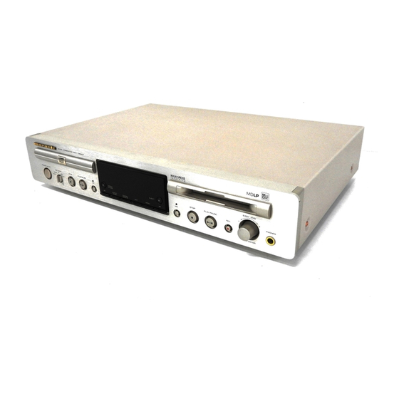
CD/MD COMBINATION DECK CM6200
PROG RANDOM DIGITAL
REPEAT
TOC
1 A- B TOTAL TRACK
CD-TEXT
STANDBY
POWER
ON/OFF
OPEN/
REC MODE
STOP
PLAY/PAUSE
CLOSE
SP
MONO
LP2
CD
TIMER
LP4
DIRECT
DUBB
TABLE OF CONTENTS
CM6200
CD/MD Combination Deck
L
AUTO SYNC
dB -50
-30
-22
-16
-12
-8
-4
0 OVER
R
EJECT
STOP
PLAY/PAUSE
MD
REC
CANCEL
EDIT
MENU
DELETE
CM6200 /
F1N, /S1G
EASY JOG
-
+
PHONES
PUSH ENTER
R
412K855010 MIT
First Issue 2001.06
Advertisement
Table of Contents

Related Manuals for Marantz CM6200/F1N


Summary of Contents for Marantz CM6200/F1N
- Page 1 Service CM6200 / F1N, /S1G Manual CD/MD Combination Deck CD/MD COMBINATION DECK CM6200 PROG RANDOM DIGITAL REPEAT AUTO SYNC dB -50 0 OVER 1 A- B TOTAL TRACK CD-TEXT STANDBY EASY JOG POWER ON/OFF OPEN/ REC MODE STOP PLAY/PAUSE EJECT STOP PLAY/PAUSE CLOSE...
- Page 2 MARANTZ Parts for your equipment are generally available to our National Marantz Subsidiary or Agent. ORDERING PARTS : Parts can be ordered either by mail or by Fax.. In both cases, the correct part number has to be specifi ed.
-
Page 3: Technical Specifications
1.1 TECHNICAL SPECIFICATIONS Specifi cations Audio characteristics Channels(SP, LP2, LP4 mode) ........................Stereo, 2 channels Monaural (MONO mode) ............................1 channel Frequency response ............................20 to 20,000 Hz Recording system ..................... Magnetic fi eld modulation override system Dynamic range..............................More than 95 dB Signal-to-noise ratio............................ -
Page 4: Service Mode
1.2 SERVICE MODE 1. FACTORY MODE The factory mode is to confi rm <FLD all illuminate>, <Microprocessor Version check>, <Button Check>. How to enter the Factory Mode 1) Press the POWER button on the front panel, while depressing the MD EJCET button and ENTER(EASY JOG) button. 2) Press the ENTER (EASY JOG), then "NO key"... -
Page 6: Taking Out The Stack Disc
1.3 TAKING OUT THE STACK DISC Taking out the disc when it stack. (For example: when it is not possible to turn on the product. The disc can not be taken out from the loader.) MD disc Remove the top cover (001D). Remove the three screws (A: 5128) and two cables (W561 and W562). -
Page 7: Block Diagram
1.4 BLOCK DIAGRAM CD disc Remove the top cover (001D). CODEC µDA1345TS Move forward the slide gear (051N) by your fi nger. <MD> +3VBAC +5VD Q501 +3VA +3VD Then the tray is moved a little. Pull the tray with your MDM-08BD AD_DATA hand at this time... -
Page 8: Schematic Diagram
1.5 SCHEMATIC DIAGRAM +5DL +5DL L201 P206 10 µH L222 R242 R241 10 µH +5AL C237 C215 R246 2.2k C236 D221 100n 6.3V +5AL 6.3V TDA1302T +5AL +5AL Q201 +5DL ISS301 GNDHF +5DL C216 R243 R214 C241 J201 VGOP C243 R213 R244 100n... - Page 9 +3VA C313 -12VA D362 Q421 C308 -12VA C362 LC4966 1SS322 Q801 F302 D421 R362 R306 LB1641 C442 1SS301 0 OHM /16V /16V J801 AINR +12VA R802 CLOSE C306 D364 R302 +5VD 220p 100k R304 1SS322 R801 OPEN C303 STOP CLOSE OPEN C801 +5VD...
- Page 10 V101 P406 2/2 F581 +3VA +3VAD OPT IN C581 GP1F32R PROG RANDOM DIGITAL +3VA +3VA /6.3V REPEAT AUTO SYNC dB -50 0 OVER R590 R589 1 A- B TOTAL TRACK R588 C590 R556 DADATA C591 CD TEXT /10V ADDATA C557 J552 C588 C592...
-
Page 11: Parts Location
1.6 PARTS LOCATION P406 Q681 Q671 Q707 Q853 - Q856 Q851 Q431 Q801 Q682 Q421 Q581 Q702 Q701 Q661 Q652 Q651 Q441 Q401 Q751 Q711 - Q713 Q612 Q301 Q404 Q403 Q692 Q691 Q613 - Q615 Q611 Q653 Q654 Q422 - Q426 Q431 D431 WG412K101-0 P406... - Page 12 P106 Q102 Q103 Q101 C102 R119 C105 UPD780204 Q101 R104 R105 C104 5MHZ R106 D101 X101 D132 V101 P106 WG412K102-0 S133 R911 R132 S126 Z911 W151 CD OPEN MD EJECT C911 MD STOP MD PLAY C912 S125 S122 R125 R124 EDIT DIR.DUBB MENU...
-
Page 13: Waveforms
1.7 WAVEFORM ( FLAG NO. ) P606 220V VOLTAGE SEL 110V BCLK P606 S602 LRCK WG412K104-0 J601 ADDATA U601 (F/S ONLY) DADATA SILB U602 5 V/Div 5 µSec 5 V/Div 0.1 mSec S TYPE K TYPE U603 U604 S601 U605 MD_DSCK MD_DSCK MD_KDATA... -
Page 14: Exploded View And Parts List
1.8 EXPLODED VIEW AND PARTS LIST 5 1 2 6 3 X8 ( M) 5 1 2 8 3 X8 ( M) x 2 W6 0 1 CASE ASSY. ( 0 5 3 N) x 2 ( 0 5 2 N) x 2 0 4 3 N ( 0 4 5 N) 5 0 0 N... - Page 15 FFC 17P 200MM 0MM PITCH YU17200520 001S PACKING CASE 412K801010 W601 F 482232111359 MAINS CORD YC01800800 003S CUSHION 386K809010 W601 S MAINS CORD YC01800620 NOTE : "nsp" PART IS LISTED FOR REFERENCE ONLY, MARANTZ WILL NOT SUPPLY THESE PARTS. 1-21...
- Page 16 1.9 ELECTRICAL PARTS LIST NOTE ON SAFETY FOR FUSIBLE RESISTOR : ASSIGNMENT OF COMMON PARTS CODES. RESISTORS The suppliers and their type numbers of fusible resistors : 1) GD05 × × × 140, Carbon film fixed resistor, ±5% 1/4W are as follows; : 2) GD05 ×...
- Page 17 4822 051 30472 CHIP 4.7kΩ ±5% 1/16W NN05472610 Z911 4822 130 11494 PHOTO UNIT PRM6936-V4 HW10004210 R216 4822 116 82487 CHIP 0Ω ±5% 1/16W NN05000610 NOTE : "nsp" PART IS LISTED FOR REFERENCE ONLY, MARANTZ WILL NOT SUPPLY THESE PARTS. 1-23...
- Page 18 4822 124 22277 ELECT. 470µF 16V M RA-2 OA47701620 NL322522-100K C620 4822 124 22277 ELECT. 470µF 16V M RA-2 OA47701620 C621 4822 124 22274 ELECT. 4.7µF M 50V RA-2 OA47505020 NOTE : "nsp" PART IS LISTED FOR REFERENCE ONLY, MARANTZ WILL NOT SUPPLY THESE PARTS. 1-24...
- Page 19 4822 051 30471 CHIP 470Ω ±5% 1/16W NN05471610 R415 4822 051 30102 CHIP 1kΩ ±5% 1/16W NN05102610 R685 4822 051 30392 CHIP 3.9kΩ ±5% 1/16W NN05392610 NOTE : "nsp" PART IS LISTED FOR REFERENCE ONLY, MARANTZ WILL NOT SUPPLY THESE PARTS. 1-25...
- Page 20 4822 116 82487 CHIP 0 OHM NN05000610 MA8075-M UDPS7.5B F401 4822 116 82487 CHIP 0 OHM NN05000610 F402 4822 116 82487 CHIP 0 OHM NN05000610 NOTE : "nsp" PART IS LISTED FOR REFERENCE ONLY, MARANTZ WILL NOT SUPPLY THESE PARTS. 1-26...
- Page 21 4822 126 11687 CER. CHIP 0.1µF DK98104200 P801-MISCELLANEOUS F851 F 4822 116 82487 CHIP 0Ω ±5% 1/16W NN05000610 F851 S 9965 000 05005 FERRIT BEADS FC90020120 BK1608HM102-T NOTE : "nsp" PART IS LISTED FOR REFERENCE ONLY, MARANTZ WILL NOT SUPPLY THESE PARTS. 1-27...
-
Page 22: Table Of Contents
Service MDM-08BD Manual MD Module TABLE OF CONTENTS SECTION PAGE 2. MDM-08BD( MD MODULE ) 2.1 MD TEST MODE..........................2-2 2.2 ADJUSTMENT............................. 2-4 2.3 DISASSEMBLY AND REPLACEMENT....................2-14 2.1 MD TEST MODE (Japan)........................2-16 2.2 ADJUSTMENT (Japan)........................2-17 2.3 DISASSEMBLY AND REPLACEMENT(Japan).................. 2-27 2.4 WAVEFORMS ............................ -
Page 23: Md Test Mode
2.1 MD TEST MODE 1. How to enter the MD TEST MODE. Turn OFF the CM6200. Press the POWER button on the front panel, while depressing the MD STOP button and ENTER(EASY JOG) button. The FL display shows [Service Mode] for seconds, then [CD/MD SELECT] will be shown on it. Press the MD button. - Page 24 6. FUNCTIONS OF BUTTONS BUTTON NOTICE COMMENT POWER Exit the TEST MODE. (by Remote control- The FL display shows ”MD TEST OFF” after EEPROM ler only) restored and mechanism adjustment. Start the disc loading. MD EJECT EJECT the MD disc. Forward the TEST MODE menus.
-
Page 25: Adjustment
2.2 ADJUSTMENT (MD module) 1. Test discs and tools 1) MD Test disc High reflection disc A-BEX TMD-381 For audio performance measurement Low reflection disc Blank disc on market for Rec/Play Eccentricity sisc A-BEX TMD-311R Confirm operation after replacing the mechanism Surface distortion disc A-BEX TMD-331R Confirm operation after replacing the mechanism... - Page 26 3. Adjustment process order 1. EJECT mode Step No. Setting Method Remarks Display Step 1 Test mode EJECT state [ _ _ E J E C T _ _ _ ] Step 2 Press the MD button. Playback power output state [ p p w _ _ _ _ _ _ _ ] Step 3 Press the MD button.
- Page 27 4. AUTO AFB adjustment mode Step No. Setting Method Remarks Display Step 1 Test mode STOP state [ t s m Step 2 Press the MENU button two times. AUTO AFB adjustment menu [ _ A U T _ A F B _ _ ] Step 3 Press once the MD PLAY button.
- Page 28 c) Tracking setting Step No. Setting Method Display Step 1 Test mode STOP state [ t s m Step 2 Press the MENU button seven times. [ E E P R O M_ S E T ] Step 3 Press the MD PLAY button. [ _ _ F o c u s _ _ _ ] Step 4 Press the MENU button two times.
- Page 29 e) TEMP setting Setting Method Display Step No. Step 1 EJECT state (or state without mechanism) [ _ _ E J E C T _ _ _ ] Step 2 Press the ENTER button. [ T E M P_ • : Setting value, : Measurement value Refer to EEPROM (IC1402) writing procedure...
- Page 30 6. TEST-REC mode With recording (Low refl ection) mini disc (For confi rmation of the playback ability at the named address.) Step No. Setting Method Remarks Display Step 1 Test mode STOP state [ t s m Step 2 Press the ENTER button two times. TEST-REC menu [ T E S T _ R E C _ _ ] Step 3...
- Page 31 Magnetic head up shift arm Rotating the loading motor forcibly The loading motor can be rotated forcibly by rotating the It is lowered ]/REW[ ] button while STOP or EJECT in the test (B1)x1 by hand. mode appears on the display. 1.7x 5mm Ø...
- Page 32 From Magnetic Head 2 Pin Extension Connector YU000820R From Mechanism Switch PWB 28 Pin Extension Flat Cable Extension PWB for service YU000850R CM6000JIG Fit the exrension PWB for service to the mechanism MD Main PWB 6 Pin Extension Flat Cable YU000830R 5 Pin Extension Flat Cable YU000840R...
-
Page 33: Eeprom Writing Procedure
EEPROM WRITING PROCEDURE EEPROM (IC1402) writing procedure 1. Method for setting the reference temperature value (This setting should be performed quickly at a room temperature, between 21 °C to 29 °C when the PWB is not hot.) 1 When replacing the EEPROM, wait until it has cooled down. 2 Connect the main unit using the single MD main PWB. - Page 34 Tracking setting Control setting Item indication Setting Item indication Setting C O N T R L 1 C O N T R L 2 T G 2 A D J T T M T F 0 H D E Q A D T F 1 L D E Q A D T F 2...
-
Page 35: Disassembly And Replacement
2.3 DISASSEMBLY AND REPLACEMENT MD MECHANISM SECTION Caution: After pulling out the optical pickup connector, wrap the end of the connector in conductive aluminium foil to prevent the optical pickup from being destroyed by static electricity.f (T1)x1 Shield Case, Top Ø2x3mm (T1)x1 Ø2x3mm... - Page 36 How to remove the magnetic head (See Fig. 15-1) (A1)x1 1. Remove the screw (A1) x 1 pc. Ø1.7x5mm Caution: Take utmost care so that the magnetic head is not damaged Magnetic Head when it is mounted. How to remove the MD loading motor PWB/MD MD Mechanism loading motor (See Fig.
- Page 37 2-16...
- Page 38 2-17...
- Page 39 2-18...
- Page 40 2-19...
- Page 41 2-20...
- Page 42 2-21...
- Page 43 2-22...
- Page 44 2-23...
- Page 45 2-24...
- Page 46 2-25...
- Page 47 2-26...
- Page 48 2-27...
- Page 49 2-28...
-
Page 50: Waveforms
2.4 WAVEFORMS OF MD CIRCUIT POWER ON TOC READ (Low reflection disc) TP1122 (F+) TP1518 (RESET) TP1207 (TEMON) TP1603 TP1800 (SP+) (3.2V) TP1602 TP1511 (SP-) (PCONT0) TOC READ (High reflection disc) TOC READ (Low reflection disc) TP1122 TP1122 (F+) (F+) TP1207 TP1212 (TEMON) - Page 51 PLAY (Low reflection disc) TP1201 (EFMMON) TP1300 (REC HEAD) TP1207 (TEMON) TP1302 (EFMO) TP1121 (T+) TP1105 (LDVAL) TP1421 (CIN) TP1113 (R/P) PLAY (High reflection disc) Analog REC TP1201 (EFMMON) IC1201 (DFCK) TP1207 (TEMON) IC1201 (ADDATA) TP1121 (T+) IC1201 (BCLK) TP1421 (CIN) IC1201 (LRCK)
-
Page 52: Ic Data
2.5 IC DATA IC1101 VHiiR3R58M/-1: RF Signal Processor (IR3R58M) Function Terminal Name Pin No. RF signal input terminal 1. Input of RF signal output of pickup. RF signal input terminal 2. Input of RF signal output of pickup. RF signal input terminal 3. Input of RF signal output of pickup. RF signal input terminal 4. - Page 53 IC1101 VHiiR3R58M/-1: RF Signal Processor (IR3R58M) ADAGI EFM AGC ADAGC DIFF ADIPNF ADIP AGC REFI ADIPO BIAS REFO GND2 AOUT VCC2 OPICPW MODE DISC SGAIN BOUT DTEMP IC1201 VHiLR37816A-1: Endec/Atrac (LR37816A) 75 74 73 72 71 70 69 68 67 66 65 64 63 62 61 60 59 58 57 56 55 54 53 52 51 TOTMON EFMO TEMCN...
- Page 54 IC1201 VHiLR37816A-1: Endec/Atrac (LR37816A) (1/2) Terminal Name Input/Output Function Pin No. EFMMON Output EFM monitor output. AVCC1 Input Analog power supply. (for EFM system 8AD, 8DA) EFMI Input EFM signal input from RF amplifi er. AGND1 Analog GND. AVCC2 Input Analog power supply.
- Page 55 IC1201 VHiLR37816A-1: Endec/Atrac (LR37816A) (2/2) Terminal Name Input/Output Function Pin No. TCRS Output Track cross signal. TEST0 Input Input for test. Connected to GND if used normally. TEST1 Input Input for test. Connected to GND if used normally. DILOCK Output DIN lock detection.
- Page 56 IC1202 RH-iX2474AFZZ: 4Mbit D-RAM (IX2474AF) Function Terminal Name Pin No. 1, 2 DQ0, DQ1 Data input/Data output. Write enable. Row address strobe. Address input. A0-A3 Address input. Power (3.3 V) 11-15 A4-A8 Address input. Output enable. Column address strobe. 18, 19 DQ2, DQ3 Data input/Data output.
- Page 57 IC1401 RH-iX0410AWZZ: MD System Microcomputer (IX0410AW) (1/2) Terminal Name Input/Output Function Pin No. 4M/16M Output 4 M/16 M DRAM selection input. Output 64 M DRAM selection input. LDVAR Output LDVAR (laser power adjustment output) ADJS Output ADJS (for automatic adjustment step check) Input CIN (track count signal input) N.C.
- Page 58 IC1401 RH-iX0410AWZZ: MD System Microcomputer (IX0410AW) (2/2) Terminal Name Input/Output Pin No. Function SYS D2 Input/Output SYS D2 (data bus 2) SYS D1 Input/Output SYS D1 (data bus 1) SYS D0 Input/Output SYS D0 (data bus 0) SLOT1 Output Input output port P37 SLOT2 Output Input/output port P36...
-
Page 59: Parts Location
2.6 PARTS LOCATION R1503 R1502 L1552 R1501 C1304 R1504 R1561 L1551 C1702 C1803 C1800 R1612 R1808 R1614 Q1800 C1802 D1401 R1801 C1303 R1803 R1802 R1806 Q1403 Q1802 Q1402 Q1806 R1424 R1440 R1536 C1409 R1435 R1622 R1623 R1621 L1101 R1263 C1125 C1616 C1264 C1263... - Page 60 P50 1 - E TO MAIN PWB CNPU04 P49 5 - E TO MAGNET HEAD P50 5 - A CW1501 CW1903 FROM MAIN PWB CW1502 TP1543 TP1702 R1505 TP1301 CN1300 CN1501 R1506 TP1521 TP1518 TP1524 CN1502 C1508 R1507 TP1517 TP1525 R1509 TP1300 TP1515...
- Page 61 MD LOADING PWB-E2 SW1934 PLAY M903 MD LOADING MOTOR TP1972 SW1933 SW1932 LOADING RECORD TP1971 TP1973 TP1974 TP1975 P59 12 - D CN1401 TO MD MAIN PWB CW1931 R1933 R1930 R1931 SW1931 DISC MEDIA P59 8 - A TO MD MAIN PWB CN1300 MAGNET HEAD(34) RECORD...
-
Page 62: Schematic Diagram
2.7 SCHEMATIC DIAGRAM 2-41 2-42... -
Page 63: Exploded View And Parts List
D1300 SBE803 HD201520R M903 D1401 SB00703Q HD201530R D1402 1SS355 HD201540R SW1934 NOTE : "nsp" PART IS LISTED FOR REFERENCE ONLY, MARANTZ WILL NOT SUPPLY THESE PARTS. SW1932 SW1933 PWB-C MISCELLANEOUS PWB-E1 XL1201 CRYSTAL 33.8688MHz JX000720R CN1101 CONNECTOR 28 PIN YJ002260R...
Need help?
Do you have a question about the CM6200/F1N and is the answer not in the manual?
Questions and answers