Table of Contents
Advertisement
Notes: 1) These model's BD Drive/Main P.C.B. Assembly are:-
- RFKNBT230P (For P);
- RFKNBT230PC (For PC);
- RFKNBT330P (For P);
- RFKNBT330PC (For PC).
2) Please refer to the original service manual for:
• Speaker system SB-BT230P-K (For SA-BT230P/PC-K), Order No: PSG1001007CE.
• Speaker system SB-BT330P-K (For SA-BT330P/PC-K), Order No: PSG1001008CE.
Caution:
Pairing of BD Drive and Main P.C.B. as "BD Drive & Main P.C.B. Assembly" have to be replaced together. If
either BD Drive or Main P.C.B. is changed, BD Drive unit has to carry out re-adjustment due to alignment
data for BD Drive Unit is stored in the Main P.C.B.
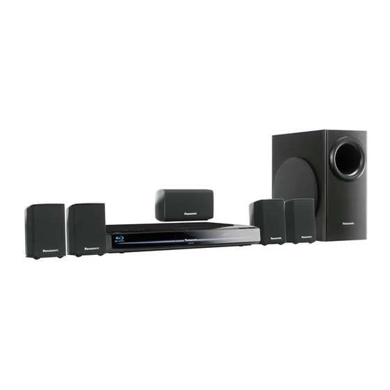
Blu-ray Disc Home Theater Sound System
Model No.
Volume 1
Product Color: (K)...Black Type
SA-BT230P
SA-BT230PC
SA-BT330P
SA-BT330PC
© Panasonic Corporation 2010. All rights reserved.
Unauthorized copying and distribution is a violation
of law.
PSG1001003CE
A6
Advertisement
Table of Contents

Related Manuals for Panasonic SA-BT230P


Summary of Contents for Panasonic SA-BT230P
- Page 1 - RFKNBT330P (For P); - RFKNBT330PC (For PC). 2) Please refer to the original service manual for: • Speaker system SB-BT230P-K (For SA-BT230P/PC-K), Order No: PSG1001007CE. • Speaker system SB-BT330P-K (For SA-BT330P/PC-K), Order No: PSG1001008CE. Caution: Pairing of BD Drive and Main P.C.B. as “BD Drive & Main P.C.B. Assembly” have to be replaced together. If either BD Drive or Main P.C.B.
-
Page 2: Table Of Contents
TABLE OF CONTENTS PAGE PAGE 1 Safety Precautions -----------------------------------------------4 10.16. Disassembly of BD Drive ------------------------------ 57 1.1. GENERAL GUIDELINES --------------------------------4 10.17. Disassembly of Main P.C.B.--------------------------- 64 1.2. Before Repair and Adjustment--------------------------4 10.18. Disassembly of D-Amp P.C.B.------------------------ 65 1.3. Protection Circuitry-----------------------------------------5 10.19. - Page 3 18.5. iPod/iPhone, Optical In & Wireless Adapter P.C.B. ------------------------------------------------------ 127 19 Terminal Function of ICs------------------------------------ 129 19.1. IC6001(C0HBB0000057): IC FL Driver ----------- 129 20 Exploded View and Replacement Parts List --------- 131 20.1. Exploded View and Mechanical replacement Part List --------------------------------------------------- 131 20.2.
-
Page 4: Safety Precautions
1 Safety Precautions 1.1. GENERAL GUIDELINES 1. When servicing, observe the original lead dress. If a short circuit is found, replace all parts which have been overheated or damaged by the short circuit. 2. After servicing, see to it that all the protective devices such as insulation barriers, insulation papers shields are properly installed. -
Page 5: Protection Circuitry
1.2.1. Caution for fuse replacement 1.3. Protection Circuitry The protection circuitry may have operated if either of the following conditions are noticed: • No sound is heard when the power is turned on. • Sound stops during a performance. The function of this circuitry is to prevent circuitry damage if, for example, the positive and negative speaker connection wires are “shorted”, or if speaker systems with an impedance less than the indicated rated impedance of the amplifier are used. -
Page 6: Safety Parts Information
1.4. Safety Parts Information Safety Parts List: There are special components used in this equipment which are important for safety. These parts are marked by ( ) in the Schematic Diagrams & Replacement Parts List. It is essential that these critical parts should be replaced with manufacturer’s specified parts to prevent shock, fire or other hazards. -
Page 7: Warning
2 Warning 2.1. Prevention of Electrostatic Discharge (ESD) to Electrostatic Sensitive (ES) Devices Some semiconductor (solid state) devices can be damaged easily by static electricity. Such components commonly are called Elec- trostatically Sensitive (ES) Devices. Examples of typical ES devices are integrated circuits and some field-effect transistors and semiconductor “chip”... -
Page 8: Precaution Of Laser Diode
2.2. Precaution of Laser Diode Caution: This product utilizes a laser diode with the unit turned “on”, invisible laser radiation is emitted from the pickup lens. Wavelength: 790 nm (CDs), 650 nm (DVDs), 405 nm (BDs) Maximum output radiation power from pickup: 100 W/VDE Laser radiation from the pickup unit is safety level, but be sure the followings: 1. -
Page 9: Service Caution Based On Legal Restrictions
2.3. Service caution based on Legal restrictions 2.3.1. General description about Lead Free Solder (PbF) The lead free solder has been used in the mounting process of all electrical components on the printed circuit boards used for this equipment in considering the globally environmental conservation. The normal solder is the alloy of tin (Sn) and lead (Pb). -
Page 10: Handling Precautions For Bd Drive
2.4. Handling Precautions for BD Drive The laser diode in the optical pickup unit may break down due to static electricity of clothes or human body. Special care must be taken avoid caution to electrostatic breakdown when servicing and handling the laser diode in the BD Drive. Figure 1 Grounding for electrostatic breakdown prevention 2.4.1. -
Page 11: Service Navigation
3 Service Navigation 3.1. Service Information This service manual contains technical information which will allow service personnel’s to understand and service this model. Please place orders using the parts list and not the drawing reference numbers. If the circuit is changed or modified, this information will be followed by supplement service manual to be filed with the original ser- vice manual. -
Page 12: Caution For Replacing Parts
Perform playback for one minute using the RAM disc. No abnormality should be seen in the picture, sound or operation. *Panasonic DVD-RAM disc should be used when recording and play- back. Perform playback for one minute using the BD-Video disc. -
Page 13: Specifications
4 Specifications Wave length: 790 nm (CDs)/650 nm (DVDs)/405 nm (BDs) Laser power: No hazardous radiation is emitted with the safety protection Main unit SA-BT230P/PC, SA-BT330P/PC TERMINAL SECTION GENERAL USB: Power supply: AC 120 V, 60 Hz USB 2.0 (Use for Wireless LAN Adaptor only) -
Page 15: Location Of Controls And Components
5 Location of Controls and Components 5.1. Remote Control Key Button Operations... -
Page 16: Main Unit Key Button Operations
5.2. Main Unit Key Button Operations... -
Page 17: Using Bd-Live Bonusview In Bd-Video
5.3. Using BD-LIVE BONUSVIEW in BD-Video... -
Page 18: Using The Ipod/Iphone
5.4. Using the iPod/iPhone... - Page 19 5.4.1. iPod /iPhone Playback...
-
Page 20: Speaker Connections
5.5. Speaker Connections... -
Page 21: Disc Playability
5.6. Disc Playability... -
Page 22: Sd Information
5.7. SD Information... -
Page 23: File Extension Type Support (Mp3/Jpeg/Avchd/Mpeg2 Files)
5.8. File Extension Type Support (MP3/JPEG/AVCHD/MPEG2 files) - Page 24 5.8.1. File Folders Structures...
-
Page 25: Operating Instructions
6 Operating Instructions 6.1. Removing of disc during abnomality 6.1.1. Using main unit key buttons. 6.1.1.1. When the power can be turned off. 1. Turn off the power and press & hold [SKIP FWD] button on remote and [OPEN/CLOSE] button on main unit for 5 seconds. 6.1.1.2. -
Page 26: Self-Diagnostic And Special Mode Setting
7 Self-Diagnostic and Special Mode Setting 7.1. Special Mode Table 1 Self-Diagnostic Function provides information for error to service personnel by Self-Diagnosis Display when any error has occurred. U**, H** and F** are stored in my memory and held. • You can check latest error code by transmitting [0] [1] of Remote Control in Service Mode. Automatic Display on FL will be cancelled when the power is turned off or AC input is turned off during self-diagnosis display is Item Key operation... -
Page 27: Special Mode Table
7.2. Special Mode Table 2 Item FL display Key operation Mode name Description Front Key Demonstration lock/ Ejection of the disc is prohibited. *When lock the tray. When the power is on, press unlock The lock setting is effective until unlocking the [PLAY] and [OPEN/CLOSE] keys tray released... -
Page 28: Error Code Table
7.3. Error Code Table 7.3.1. Error Code Table (For BD) Error Code Diagnosis contents Description Monitor Display Automatic FL display Remote control code error Display appears when main unit and remote No display controller codes are not matched. is remote controller code of the main unit. - Page 29 7.3.2. Error Code Table 2 (For BD) Error Code Diagnosis contents Description Monitor Display Automatic FL display SELF Restoration operation Since the power cord fell out during a power No display SELF CHECK CHECK failure or operation, it is under restoration operation.
-
Page 30: Service Mode
7.4. Service Mode To enter service mode: While the power is off, press & hold [VOL+] & [OPEN/CLOSE] button on main unit for 3 secs or more follow by [PLAY] button on main unit. 7.4.1. Service Mode Table 1 Item FL display Key operation Mode name... - Page 31 7.4.2. Service Mode Table 2 Item FL display Key operation Mode name Description (Remote controller key) Laser Used Time Check laser used time (hours) of drive. Press [4] [1] in service mode. Indication ****** (******) is the used time display in hour.
- Page 32 7.4.3. Service Mode Table 3 Item FL display Key operation Mode name Description (Remote controller key) BD/DVD drive last error BD/DVD drive error code display. 1. Error Number is displayed for 5 Press [4] [2] in service mode. seconds. **** 2.
- Page 33 7.4.4. Service Mode Table 4 Item FL display Key operation Mode name Description (Remote controller key) In case that the maker cannot be 6. Disc maker ID is displayed for 5 identified, display is black out. seconds. 7. Factor of drive error (hexadeci- mal) occurring is left displayed.
- Page 34 7.4.5. Service Mode Table 5 Item FL display Key operation Mode name Description (Remote controller key) CEC (H) output Check of the CEC terminal high output of Press [5] [5] in service mode. HDMI. CECHOK CECHNG CEC (L) output Check of the CEC terminal low output of Press [5] [6] in service mode.
-
Page 35: Troubleshooting Guide
8 Troubleshooting Guide 8.1. Troubleshooting Guide for F61 and/or F76 Symptom Checking items Possible Fault(s) Remarks Set cannot ON Faulty AC Cord,Loose connection AC Cord Refer to P5701 soldier crack,dry joint,etc. AC Inlet P5701 SMPS F1 fuse open Fuse F1 P.C.B. - Page 36 8.1.1. SMPS P.C.B. Photocouple: Switching IC: IC5799 PC5702, D5799 FUSE: F1 Rectifier: D5802 Switching IC: IC5701 Transformer: T5701 Figure 1. SMPS P.C.B.
- Page 37 8.1.2. Power P.C.B. (Side A of Power P.C.B.) Q2903 Q2902 IC2901 (Side B of Power P.C.B.) CN2916, CN2917, L2902 L2907 L2908 Fig 2. Power P.C.B.
- Page 38 8.1.3. Main P.C.B. CN2004 IC2302, LB2301 Fig 3. Main P.C.B.
-
Page 39: Service Fixture & Tools
9 Service Fixture & Tools 9.1. Service Tools and Equipment Prepare service tools before process service position. Service Tools Remarks SMPS P.C.B. (*JW1) - Main P.C.B. (CN2004) RFKZBT230P (18P FFC) Main P.C.B. (CN2006) - D-Amp P.C.B. (CN5402) REXX1037 (10P Cable) -
Page 40: Disassembly And Assembly Instructions
10 Disassembly and Assembly Instructions Caution Note: • This section describes the disassembly and/or assembly procedures for all major printed circuit boards & main compo- nents for the unit. (You may refer to the section of “Main components and P.C.B Locations” as described in the service manual) •... -
Page 41: Disassembly Flow Chart
10.1. Disassembly Flow Chart 10.3.Top Cabinet 10.4. AC Inlet P.C.B. 10.16.BD Drive 10.8. Front Panel Block 10.9. Panel P.C.B. 10.20. Power P.C.B. 10.5. Optical In P.C.B. 10.10. Power Button 10.6. Wireless Adapter 10.21. SMPS P.C.B. P.C.B. P.C.B. 10.22. Switching Regulator 10.11. -
Page 42: Main Components And P.c.b. Locations
10.2. Main Components and P.C.B. Locations... -
Page 43: Disassembly Of Top Cabinet
10.3. Disassembly of Top Cabinet Step 1 Remove 2 screws. Step 2 Remove 3 screws. Step 5 Press down the catches one by one. Caution: To avoid shocked by electricity & injured by high temperature. DO NOT TOUCH electrical components when insert hand under the Top Cabinet. -
Page 44: Disassembly Of Ac Inlet P.c.b
Step 1 Remove 1 screw. Step 2 Twist the Wire Holder. Step 3 Release Red(TL10) & Black(TL20) wires from the Wire Holder. Caution: During assembling, ensure that catches of Top Caution: During assembling, ensure that Red (TL10) & Cabinet is insert into Front Panel properly. Black(TL20) wires are dressed into Wire Holder. -
Page 45: Disassembly Of Optical In P.c.b
10.5. Disassembly Optical P.C.B. • Follow (Step 1) to (Step 6) of Item 10.3. Step 1 Remove 2 screws. Step 2 Detach 13P FFC at the connector (CN4002) on Optical 10.6. Disassembly Wireless In P.C.B.. Adapter P.C.B. • Follow (Step 1) to (Step 6) of Item 10.3. Step 1 Remove 1 screw. -
Page 46: Disassembly Of Rear Panel
Caution: During assembling, ensure that Wireless Adapter P.C.B. is seated properly at the locators & fully catched onto Transmitter Chassis. Step 7 Remove Wireless Adapter P.C.B.. Step 4 Detach 17P FFC at the connector (CN3001) on Wire- less Adapter P.C.B.. 10.7. -
Page 47: Disassembly Of Front Panel Block Assembly
Caution: During assembling, ensure that 15P FFC is dressed through Front Shield. Step 5 Release the tabs on both side of the Rear Panel in the direction of arrow. Step 3 Release the tabs on both side of the Front Panel Block Assembly in the direction of arrow. -
Page 48: Dissassembly Of Panel P.c.b
Caution: Do not exert strong force when releasing the tabs. Step 2 Release 1 catch. Step 5 Detach the Front Panel Block Assembly. Step 3 Lift up the Panel P.C.B.. 10.9. Dissassembly of Panel P.C.B. • Refer to “Disassembly of Front Panel Block Assembly”. •... -
Page 49: Dissassembly Of Power Button P.c.b
Step 4 Fix 5 screws. • Assembly of Panel P.C.B Step 1 Solder the 4P cable to the connector (CN6001) on Panel P.C.B.. Step 5 Dress 4P cable into the Front Panel’s ribs according to diagram shown. Step 2 Dress 22P FFC according to diagram shown. Step 3 Place the Panel P.C.B. - Page 50 Step 2 Fix the Power Button P.C.B. onto the Front Panel. Caution: Ensure that it is properly located & seated prop- erly. Step 2 Lift up the Power Button P.C.B.. Step 3 Fix 1 screw. Step 3 Desolder the 4P Cable (H6803) on Power Button P.C.B..
-
Page 51: Replacement Of Cradle Lid
10.11. Replacement of Cradle Lid • Refer to “Disassembly of Front Panel Block Assembly”. 10.11.1. Disassembly of Cradle Lid Step 1 Release the Cradle Lid Spring by using a flat head screw driver in the direction of arrow. Step 5 Dress 4P cable into Front Panel’s U-Slot & ribs accord- ing to diagram shown. - Page 52 Step 4 Rotate the Cradle Lid about 45 according to the dia- Step 2 Slightly push the Cradle Lid inwards. gram shown. Step 3 Press the Cradle Lid downward. Step 5 Remove Cradle Lid. 10.11.2. Assembly of Cradle Lid Step 1 Insert the Cradle Lid (Shaft A) into the Front Panel (Slot A &...
-
Page 53: Replacement Of Ipod Cradle Assembly
Step 5 Lift up the iPod Cradle Assembly on both sides. 10.12. Replacement of iPod Cradle Assembly • Refer to “Disassembly of Front Panel Block Assemb- ley”. 10.12.1. Disassembly iPod Cradle Assembly Step 6 Press to release iPod Cradle Assembly from Front Step 1 Detach 15P FFC at the connector (CN1002) on iPod Panel as arrow shown. -
Page 54: Disassembly Of Ipod/Iphone P.c.b
Step 3 Press the catch on the iPod Cradle Assembly. Step 4 Fix 1 screw. 10.12.2. Assembly of iPod Cradle Assembly Step 1 Fix the iPod Cradle Assembly to Front Panel. 10.13. Disassembly of iPod/iPhone Step 2 Press the iPod Cradle Assembly downwards. P.C.B. -
Page 55: Replacement Of Dvd Lid Unit
Caution: During assembling, ensure that iPod/iPhone P.C.B. is seated properly at the locators. Step 3 Lift the DVD Lid Spring at Shaft A in the direction of arrow. 10.14. Replacement of DVD Lid Unit • Refer to “Disassembly of Front Panel Block Assembly”. 10.14.1. - Page 56 Step 6 Move the DVD Lid Unit to remove from Front Panel. Step 3 Insert the DVD Lid Unit (Shaft B) into the Front Panel (Slot B) as arrow shown. 10.14.2. Assembly of DVD Lid Unit Step 1 Insert the DVD Lid Unit into the Front Panel as arrow shown.
-
Page 57: Disassembly Of Front Shield
Caution: Ensure that the Shaft B of DVD Lid Unit is fully inserted into Slot B of Front Panel. 10.15. Disassembly of Front Shield • Refer to “Disassembly of Front Panel Block Assembly”. Caution: During assembling, ensure that Front Shield is properly inserted &... - Page 58 Step 2 Detach 18P FFC at the connector (P55002) on Main Caution: During assembling, ensure that 18P FFC is inserted under Main P.C.B. Shield properly. P.C.B.. Step 3 Remove 4 screws. 10.16.1. Replacement of Upper Base Ass’y Step 1 Remove the 4 screws (A), and push the Hook in. Step 2 Lift up the Upper Base Ass’y, and pull it out to the direc- Step 4 Lift up to remove the BD Drive.
- Page 59 Then the one side of the tray is come off from the Drive. Step 5 Insert the Eject Pin into the Tray as below figure, lift up 10.16.2. Replacement of Tray the lever using the Eject Pin while pushing the dotted point of Step 1 Perform the step “10.16.1.
- Page 60 Step 3 Remove the Pulley Gear and Belt. Caution: Though the Drive P.C.B. is not supplied as replacement parts, it must be removed for after disassem- bling. Step 6 Open the connector lock, and disconnect the FFC. Step 7 Remove the 2 Screws (C), and remove the Traverse Base Ass’y with spreading the 2 hooks to the direction of arrows.
- Page 61 10.16.5. Replacement of Mid Gear, Drive Gear and Loading Motor Step 1 Perform the step “10.16.4. Slide Cam”. Step 2 Remove the Mid Gear and Drive Gear. Step 3 Remove the Screw (D) to remove the Loading Motor. Step 4 Remove the Screw (E), and remove the SW P.C.B. with the Loading Motor.
- Page 62 10.16.6. Applying Grease...
- Page 63 10.16.7. Cleansing the Lens of Optical Pick-UP Follow the “10.27.1. Upper Base Ass’y.
-
Page 64: Disassembly Of Main P.c.b
10.17. Disassembly of Main P.C.B. Step 9 Detach 10P cable at the connector (CN2004) on Main P.C.B.. • Follow (Step 1) to (Step 6) of Item 10.3. Caution: During assembling, ensure that 10P cable is prop- • Follow (Step 1) to (Step 6) of Item 10.8. erly bend down onto Digital P.C.B. -
Page 65: Disassembly Of D-Amp P.c.b
Caution: During assembling, ensure that Main P.C.B. is seated properly at the locators. Step 13 Lift up to remove Main P.C.B.. 10.18. Disassembly of D-Amp P.C.B. • Follow (Step 1) to (Step 6) of Item 10.3. • Follow (Step 1) to (Step 4) of Item 10.4. Step 1 Lift Up 2 Wire Clampers. - Page 66 Step 7 Slightly lift up to remove D-Amp P.C.B.. Step 4 Remove 2 screws on D-Amp P.C.B.. Caution: During assembling, ensure that D-Amp P.C.B. is seated properly at the locators. Step 5 Remove 4 screws. Step 6 Release the tab of the side of the Rear Panel in the direction of arrow.
-
Page 67: Replacement Of Digital Amplifier Ic (Ic5100/ Ic5200)
10.19. Replacement of Digital Ampli- fier IC (IC5100/IC5200) • Refer to “Disassembly of D-Amp P.C.B.”. 10.19.1. Disassembly of Digital Amplifier IC (IC5100/IC5200) Step 1 Place the D-Amp P.C.B. on an insulated material. Step 2 Remove 3 screws. 10.19.2. Assembly of Digital Amplifier IC (IC5100/IC5200) Step 1 Mount the Digital Amplifier IC (IC5100) onto the D-Amp P.C.B.. -
Page 68: Disassembly Of Power P.c.b
Caution: During assembling, ensure that heatsink spacer Caution: During assembling, ensure that Power P.C.B. is is seated properly onto Amp Heatsink. properly inserted & fully connected to SMPS P.C.B.. Caution: Ensure that D-Amp P.C.B. is properly located and fixed on to Amp Heatsink before screwing. Step 5 Fix 3 screws. - Page 69 Caution: Do not exert strong force when releasing the tabs. Caution: During assembling, ensure that 10P cable is bend down properly as diagram shown. Step 3 Detach the Front Panel slightly forward. Step 7 Remove 5 screws. Step 4 Lift up the Wire Clampers. Step 5 Detach 6P Cable at the connector (CN5400) on D-Amp P.C.B..
-
Page 70: Replacement Of Switching Regulator Ic (Ic5701)
Caution: During releasing P.C.B. Spacer, as it may lead to electric shock or injuries due to high temperature avoid touching surrounding electrical parts. 10.22. Replacement of Switching Reg- ulator IC (IC5701) Step 9 Lift up SMPS P.C.B.. • Refer to “Disassembly of SMPS P.C.B.”. 10.22.1. -
Page 71: Replacement Of Rectifier Diode (D5702)
Step 2 Remove 1 screw from the Switching Regulator IC Caution: Ensure pins of the Switching Regulator IC (IC5701) are properly seated and soldered on SMPS P.C.B.. (IC5701). Step 3 Remove the Switching Regulator IC (IC5701). Caution: Avoid touching the Heatsink Unit B due to its high temperature after prolonged use. - Page 72 10.23.2. Assembly Rectifier Diode (D5702) Step 1 Apply grease to the Heatsink Unit B. Step 2 Fix and screw the Rectifier Diode (D5702) to the Heat- sink Unit B. Caution: Ensure the Rectifier Diode (D5702) is tightly screwed to the Heatsink Unit B. Step 3 Mount the Heatsink Unit B with Rectifier Diode (D5702) onto SMPS P.C.B..
-
Page 73: Replacement Of Regulator Diode (D5802)
Caution: Ensure pins of the Rectifier Diode (D5702) are properly seated before soldered onto SMPS P.C.B.. Step 2 Remove 1 screw from the Regulator Diode (D5802). Step 3 Remove the Regulator Diode (D5802) from the SMPS P.C.B.. Caution: Avoid touching the Heatsink Unit A due to its high temperature after prolonged use. -
Page 74: Replacement Of Regulator Diode (D5803)
Caution: Ensure the Regulator Diode (D5802) is tightly screwed to the Heatsink Unit A. Step 4 Solder pins of the Regulator Diode (D5802) on the sol- der side of SMPS P.C.B.. Caution: Ensure pins of the Regulator Diode (D5802) are properly seated before soldered onto SMPS P.C.B.. -
Page 75: Disassembly Of Fan
Caution: Ensure the Regulator Diode (D5803) is tightly screwed to the Heatsink Unit A. Step 4 Solder pins of the Regulator Diode (D5803) on the sol- der side of SMPS P.C.B.. Caution: Ensure pins of the Regulator Diode (D5803) are Step 3 Remove 2 screws. - Page 76 Caution: During assembling, ensure Fan Unit is properly Caution: During assembling, ensure that 3P Wire is posi- located & fully catched onto Rear Panel. tioned as diagram shown. Step 5 Remove 2 screws. Step 6 Lift up to remove Fan.
-
Page 77: Service Position
11 Service Position Note: For description of the disassembly procedures, see the Section 10. 11.1. Checking & Repairing Side B of Main P.C.B. Caution: Pairing of BD Drive and Main P.C.B. as “BD Drive & Main P.C.B. Assembly” have to be replaced together. If either BD Drive or Main P.C.B. - Page 78 Step 14 Remove 1 screws. Step 11 Remove 5 screws. Step 15 Lift up Power Button P.C.B.. Step 12 Release 1 catch. Step 16 Connect extension 18P FFC RFKZBT230P from CN2006 to CN5402. Step 17 Attach 10P cable REXX1037 from CN2004 to JW2. Step 13 Lift up FL P.C.B..
-
Page 79: Checking & Repairing D-Amp P.c.b
Step 18 Slightly lift up Main P.C.B. according to diagram Step 21 Flip Main P.C.B. as diagram shown. shown. Step 22 Proceed to check and repair Side A of Main P.C.B.. Caution: Insulated material is required to insulate Main P.C.B. from other parts. 11.3. - Page 80 11.3.2. Checking & Repairing of Side A of D-Amp P.C.B. Step 1 Remove Top Cabinet. Step 2 Lift up the Wire Clamper. Step 6 Remove 6 screws. Step 3 Detach the Fan Unit connector (CN5401) on D-Amp Step 7 Remove Fan Unit according to arrow shown. P.C.B..
-
Page 81: Checking & Repairing Smps P.c.b
Step 12 Flip the D-Amp P.C.B. and position it according to dia- gram shown. Step 3 Release the 2 tabs at each side of the Front Panel Block Step 13 Connect Fan Unit to connector (CN5401) on D-Amp Assembly in the direction of arrow. P.C.B.. - Page 82 Step 5 Remove 1 screw. Step 6 Twist the Wire Holder. Step 7 Release Red(TL10) & Black (TL20) wires from the Wire Holder. Step 8 Remove AC Inlet P.C.B. from Rear Panel. Step 10 Remove 5 screws. Step 9 Twist the Wire Clampers to release 6P cable (SMPS P.C.B.
-
Page 83: Checking & Repairing Fl P.c.b
Step 4 Release 1 catch. Step 12 Flip the SMPS P.C.B. and position it according to dia- gram shown. Step 13 Proceed to check and repair SMPS P.C.B.. Step 5 Lift up FL P.C.B.. 11.5. Checking & Repairing FL P.C.B. Step 1 Remove Top Cabinet. - Page 84 Step 7 Lift up Power Button P.C.B.. Step 8 Connect 22P FFC to the connector (CN2002) on Main P.C.B.. Step 9 Proceed to check and repair FL P.C.B..
-
Page 85: Voltage & Waveform Chart
MODE CD PLAY STANDBY IC2201 REF NO. MODE CD PLAY -6.8 STANDBY -6.8 IC2202 REF NO. MODE CD PLAY -6.8 STANDBY -6.8 IC2300 REF NO. MODE CD PLAY STANDBY REF NO. IC2300 MODE CD PLAY STANDBY SA-BT230P/PC, SA-BT330P/PC MAIN P.C.B. -
Page 86: Main P.c.b. (2/3)
REF NO. MODE CD PLAY STANDBY IC2800 REF NO. MODE CD PLAY -6.8 STANDBY -6.8 IC2952 REF NO. MODE CD PLAY STANDBY IC3953 REF NO. MODE CD PLAY STANDBY REF NO. IC7002 MODE CD PLAY STANDBY SA-BT230P/PC, SA-BT330P/PC MAIN P.C.B. -
Page 87: Main P.c.b. (3/3)
REF NO. MODE CD PLAY -3.0 -1.6 -1.6 11.4 11.4 10.7 STANDBY -3.0 -1.6 -1.6 11.4 11.4 10.7 QR1102 QR7001 QR7014 QR7019 QR7071 REF NO. MODE CD PLAY STANDBY REF NO. QR7081 MODE CD PLAY STANDBY SA-BT230P/PC, SA-BT330P/PC MAIN P.C.B. -
Page 88: Panel P.c.b
REF NO. MODE CD PLAY -21.4 -21.4 STANDBY -21.4 -21.4 Q6100 Q6800 REF NO. MODE CD PLAY STANDBY SA-BT230P/PC, SA-BT330P/PC PANEL P.C.B. 12.5. Panel P.C.B. (For BT330P/PC only) IC6531 REF NO. MODE CD PLAY -7.0 STANDBY -7.0 Q6531 Q6532 Q6533 Q6534 REF NO. -
Page 89: D-Amp P.c.b. (1/2)
CD PLAY STANDBY REF NO. IC5400 MODE CD PLAY 13.1 13.1 11.6 STANDBY 13.1 13.1 11.6 IC5401 REF NO. MODE CD PLAY STANDBY IC5402 REF NO. MODE CD PLAY STANDBY IC5404 REF NO. MODE CD PLAY STANDBY SA-BT230P/PC, SA-BT330P/PC D-AMP P.C.B. -
Page 90: D-Amp P.c.b. (2/2)
42.4 Q5414 QR5400 QR5401 REF NO. MODE CD PLAY 12.0 STANDBY 12.0 SA-BT230P/PC, SA-BT330P/PC D-AMP P.C.B. 12.8. Power P.C.B. IC2901 REF NO. MODE CD PLAY 16.4 11.2 14.9 14.3 16.5 16.5 15.8 STANDBY 16.4 11.2 14.9 14.3 16.5 16.5 15.8... -
Page 91: Smps P.c.b
-14.0 -15.0 -14.6 -13.1 -15.1 -15.0 -15.0 IC5801 REF NO. MODE CD PLAY 18.3 STANDBY 18.3 IC5899 REF NO. MODE CD PLAY STANDBY REF NO. Q5720 Q5863 Q5898 Q5899 QR5862 MODE CD PLAY -10.3 -9.9 -10.2 STANDBY -10.3 -9.9 -10.2 SA-BT230P/PC, SA-BT330P/PC SMPS P.C.B. -
Page 92: Waveform Table
12.10. Waveform Table 5.6Vp-p(2usec/div) 4Vp-p(5usec/div) 4.4Vp-p(500nsec/div) 1Vp-p(10usec/div) 3Vp-p(10usec/div) 3.6Vp-p(50nsec/div) 2Vp-p(50nsec/div) 0.24Vp-p(1msec/div) 2.2Vp-p(1msec/div) 0.24Vp-p(1msec/div) 0.08Vp-p(500nsec/div) 5.2Vp-p(1usec/div) 80Vp-p(1usec/div) 5.6Vp-p(1usec/div) 6.8Vp-p(1usec/div) 76Vp-p(1usec/div) 3.6Vp-p(500nsec/div) 6Vp-p(1usec/div) 1.5Vp-p(2usec/div) 3.2Vp-p(2usec/div) -
Page 93: Illustration Of Ics, Transistor And Diode
13 Illustration of ICs, Transistor and Diode C0ABBA000159 (8p) C0DBAYH00007 (8p) C0HBB0000057 (44p) MFI341S2164 (20p) AN41215A-VF (56p) VUEALLPT040 (20p) C0ABBB000189 (8p) C0ZBZ0001726 (48p) C0FBAK000026 (16p) RFKWMBT230P C0ABBB000179 (8p) C1CB00003239 (48p) C0JBAR000540 (16p) (100p) C0DBZYY00018 (8p) MN864704AKP (128p) C0DBAYY00729 (20p) C0DBAYY00480 (24p) C1AB00002461 (30p) No.1 C1AB00003260 (36p) -
Page 95: Block Diagram
FOR BT330P/PC Q1103 UART RX CN1101 CN1002 CN1001 UART RX 36 SWITCH PANEL P.C.B. QR1102 P6001 CN2002 ASS IN FROM/TO PCONT SWITCH iPod/iPhone P.C.B. ASS IN MAIN(AUDIO) P6001 CN2002 ASS MUTE ASS MUTE PCONT PCONT 50 SA-BT230P/PC,SA-BT330P/PC MAIN(SYSTEM CONTROL) BLOCK DIAGRAM... -
Page 96: Main(Audio)
OPT IN 3 OPTICAL IN P.C.B. FOR BT330P/PC PANEL P.C.B. JK6502 ASS SW MAIN(SYSTEM CONTROL) SETUP MIC P6001 CN2002 AUTO SETUP FROM/TO SPEAKER CIRCUIT P6001 CN2002 MAIN(SYSTEM CONTROL) ACS MUTE IC6531 C0ABBB000189 OP-AMP Q6531, Q6532, Q6533, Q6534 SA-BT230P/PC,SA-BT330P/PC MAIN(AUDIO) (1/2) BLOCK DIAGRAM... - Page 97 CN3000 WIRELESS ADAPTER P.C.B. TO MAIN(AUDIO) SECTION (1/2) DSP RESET RESETX 12 DSP RESET DSP MUTE MUTEX 13 DSP MUTE FROM/TO DSP CLK DSP CLK MAIN(SYSTEM CONTROL) SCL 14 DSP DA SDA 15 DSP DA SA-BT230P/PC,SA-BT330P/PC MAIN(AUDIO) (2/2) BLOCK DIAGRAM...
-
Page 98: Digital Audio
Q5408, Q5409, Q5414 Q5400,Q5401 Q5402,Q5403 Q5404,Q5405 FAN DC OUT CN5401 FAN CONTROL CN2006 CN5402 FAN SIGNAL CIRCUIT CN5401 FAN LOCK FROM/TO MAIN(SYSTEM CONTROL) QR5401 DC DETECT CN2006 CN5402 ECO CIRCUIT FROM POWER SUPPLY DCDET (MAIN SECTION) SA-BT230P/PC,SA-BT330P/PC DIGITAL AUDIO BLOCK DIAGRAM... -
Page 99: Power Supply(Main Section)
VOUT 4 D5405 CN5402 CN2006 CN5400 +51V +55V DIGITAL AUDIO PVDD D5407 DCDET DIGITAL AUDIO PC5720 FEED BACK FROM FEED BACK POWER CONT JW2* CN2004 CIRCUIT MAIN(SYSTEM CONTROL) IC5801 C0DABFC00002 SHUNT REGULATOR Q5863 COLD SA-BT230P/PC,SA-BT330P/PC POWER SUPPLY(MAIN SECTION)(1/2) BLOCK DIAGRAM... - Page 100 D7035 D7016 Q1104 IC1001 C0DBZHE00026 CN1101 CN1002 CN1001 HIGH SIDE iPod CTRL SW SWITCH SWITCH D7017 D7036 CN1101 CN1002 CN1001 1 IN OUT 5 BATTPCONT 3 EN OC 4 FROM/TO MAIN(SYSTEM CONTROL) iPod OC SA-BT230P/PC,SA-BT330P/PC POWER SUPPLY(MAIN SECTION)(2/2) BLOCK DIAGRAM...
-
Page 101: Wiring Diagram
DOCK FOR iPod/iPhone SPEAKERS (SOLDER SIDE) DIGITAL P5701 AUDIO IN CENTER H6803 CN1001 OPTICAL 1 OPTICAL 2 AC IN SUBWOOFER 120V 60Hz TL20* TL10* CN1002 CN4002 JK3100 JK3101 NOTE: " * " REF IS FOR INDICATION ONLY. SA-BT230P/PC, SA-BT330P/PC WIRING CONNECTION... -
Page 103: Schematic Diagram Notes
16 Schematic Diagram Notes • Voltage and signal line :+B signal line • This schematic diagram may be modified at any time :-B signal line with the development of new technology. Notes: :Audio output signal line S6002: Stop switch ( S6003: Play switch ( S6005:... -
Page 105: Schematic Diagram
FE: MAIN(BP1 FE): SCHEMATIC DIAGRAM - 11 ~ 14 PE: MAIN(BP1 PERI): SCHEMATIC DIAGRAM - 15 ~ 16 TO MAIN(MICON) VO: MAIN(VIDEO OUT): SCHEMATIC DIAGRAM - 17 SECTION (4/6) MA: MAIN(MICON): SCHEMATIC DIAGRAM - 18 ~ 23 SA-BT230P/PC,SA-BT330P/PC MAIN(MICON) CIRCUIT TN: MAIN(TUNER): SCHEMATIC DIAGRAM - 24... - Page 106 GND_3 PW_DC5V_D PW_DC5V_D PE: MAIN(BP1 PERI): SCHEMATIC DIAGRAM - 15 ~ 16 TO MAIN(MICON) VO: MAIN(VIDEO OUT): SCHEMATIC DIAGRAM - 17 SECTION (5/6) MA: MAIN(MICON): SCHEMATIC DIAGRAM - 18 ~ 23 SA-BT230P/PC,SA-BT330P/PC MAIN(MICON) CIRCUIT TN: MAIN(TUNER): SCHEMATIC DIAGRAM - 24...
- Page 107 DC DETECT APD_R B0BC7R5A0266 C2202 R2204 PW_A+7V 100K PW_DC5V_DR TO MAIN(MICON) PW_A-7V QR7019 SECTION (2/6) LB7012 B1GBCFJJ0051 J0JHC0000107 D7020 B0ACCK000005 DC DETECT D7021 B0ACCK000005 C7019 C7058 6.3V1000 D7038 B0BC013A0269 LB7013 J0JHC0000107 PW_DC12V_DR C7020 16V470 TO MAIN(MICON) SECTION (6/6) SA-BT230P/PC,SA-BT330P/PC MAIN(MICON) CIRCUIT...
- Page 108 SWITCH 100K LB1108 R1101 330K R1103 220K iPod/iPhone iPod_ACC LB1101 J0JYC0000070 CIRCUIT (CN1002) iPod_5V DOCK_L LB1109 IN SCHEMATIC DOCK_L J0JCC0000316 DIAGRAM - 34 DOCK_AGND DOCK_R DOCK_R iPod_DET LB1103 iPod_DET VGND VIDEO LB1102 VGND C1134 C1131 1000P 1000P SA-BT230P/PC,SA-BT330P/PC MAIN(MICON) CIRCUIT...
- Page 109 FE: MAIN(BP1 FE): SCHEMATIC DIAGRAM - 11 ~ 14 PE: MAIN(BP1 PERI): SCHEMATIC DIAGRAM - 15 ~ 16 VO: MAIN(VIDEO OUT): SCHEMATIC DIAGRAM - 17 MA: MAIN(MICON): SCHEMATIC DIAGRAM - 18 ~ 23 TN: MAIN(TUNER): SCHEMATIC DIAGRAM - 24 SA-BT230P/PC,SA-BT330P/PC MAIN(MICON) CIRCUIT...
- Page 110 FE: MAIN(BP1 FE): SCHEMATIC DIAGRAM - 11 ~ 14 PE: MAIN(BP1 PERI): SCHEMATIC DIAGRAM - 15 ~ 16 VO: MAIN(VIDEO OUT): SCHEMATIC DIAGRAM - 17 MA: MAIN(MICON): SCHEMATIC DIAGRAM - 18 ~ 23 TN: MAIN(TUNER): SCHEMATIC DIAGRAM - 24 SA-BT230P/PC,SA-BT330P/PC MAIN(MICON) CIRCUIT...
- Page 111 FE: MAIN(BP1 FE): SCHEMATIC DIAGRAM - 11 ~ 14 PE: MAIN(BP1 PERI): SCHEMATIC DIAGRAM - 15 ~ 16 VO: MAIN(VIDEO OUT): SCHEMATIC DIAGRAM - 17 MA: MAIN(MICON): SCHEMATIC DIAGRAM - 18 ~ 23 TN: MAIN(TUNER): SCHEMATIC DIAGRAM - 24 SA-BT230P/PC,SA-BT330P/PC MAIN(TUNER) CIRCUIT...
-
Page 112: Panel Circuit
R6023 R6024 1.2K 1.5K 2.2K 3.3K 4.7K FOR BT330P/PC S6807 S6007 R6025 FOR BT230P/PC OPEN/CLOSE SELECTOR CN6001 DGND L6007 J0JBC0000014 DGND POWER BUTTON KEY1 L6006 J0JBC0000014 KEY1_BTN CIRCUIT (H6803) L6005 IN SCHEMATIC LED_VREF LED_VREF DIAGRAM - 33 SA-BT230P/PC,SA-BT330P/PC PANEL CIRCUIT... - Page 113 R6540 2.2K OP-AMP Q6534 B1GDCFGA0018 R6546 MUTING CONTROL 1.8K ACS_MUTE Q6533 B1GDCFGA0018 MUTING CONTROL C6537 R6532 150P D6532 Q6531 R6544 B0ACCK000012 B1ABEB000002 MUTING C6536 R6545 150K R6541 D6533 2.2K R6533 C6538 D6531 C6535 B0BC5R1A0266 R6543 C6534 B0ACCK000012 SA-BT230P/PC,SA-BT330P/PC PANEL CIRCUIT...
-
Page 114: D-Amp Circuit
DAP_SCL_2 FRONT L - RESERVED DAP_LRCLK DAP_SCLK FRONT L + TO SPEAKERS LRCLK SCLK FRONT R - FRONT R + CENTER - CENTER + SUBWOOFER - SUBWOOFER + IC5405 C0JBAA000501 AND GATE VALID1 TO D-AMP SECTION (3/4) SA-BT230P/PC,SA-BT330P/PC D-AMP CIRCUIT... - Page 115 R5445 D5620 1000P SPK_GND 35V470 B0HCSP000001 D5512 B0ACCK000005 D5619 L5106 B0HCSP000001 G0B9R5K00005 R5136 100K C5156 C5143 R5125 R5452 1000P 35V330 R5135 5.6K 100K 5.6K C5142 C5157 C5144 1000P 35V470 D5618 D5510 B0HCSP000001 B0ACCK000005 TO D-AMP SA-BT230P/PC,SA-BT330P/PC SECTION (4/4) D-AMP CIRCUIT...
- Page 116 B0BC7R5A0268 C5437 C5418 R5438 16V22 6.3V100 220K R5428 D5404 R5424 R5435 Q5405 B0ACCK000005 Q5412 B1ABCF000011 B1ABCF000011 SWITCH R5437 R5427 D5403 C5423 R5423 C5417 D5402 B0ACCK000005 16V10 B0BC012A0269 4.7K DC DETECT 100K C5424 5600P TO D-AMP SECTION (4/4) SA-BT230P/PC,SA-BT330P/PC D-AMP CIRCUIT...
- Page 117 C5204 C5205 C5231 0.01 C5237 C5228 R5215 1000P R5220 0.47 100K R5214 D5611 B0HCSP000001 C5230 1000P C5238 C5232 1000P 0.01 PVDD D5610 B0HCSP000001 D5628 D5627 R5474 B0BC012A0269 B0ACCK000005 C5450 R5473 R5472 16V22 6.8K TO D-AMP SECTION (3/4) SA-BT230P/PC,SA-BT330P/PC D-AMP CIRCUIT...
-
Page 118: Smps Circuit
PCONT PCONT DC_18V R5805 DC18V 6.8K DC12V MAIN(MICON) PGND Q5863 CIRCUIT (CN2004) B1ABGC000001 R5819 IN SCHEMATIC R5728 DC5V SWITCH R5817 DIAGRAM - 20 DCDET 2.2K DCDET SYS5V SYS6V SYNC R5861 C5869 C5828 R5818 SYNC 6.3V2200 100K 0.01 SA-BT230P/PC,SA-BT330P/PC SMPS CIRCUIT... - Page 119 2.2K C5725 TO SMPS C5720 OLP/SS 1000P R5733 C5700 SECTION (1/2) D5705 1000P B0BC020A0267 D5710 ZJ5702 B0EAMM000057 C5722 C5724 C5730 1000P R5732 D5713 1000P B0BC030A0264 C5721 C5726 C5747 D5708 220P 50V10 3300P B0ACCK000005 R5726 R5727 0.15 0.15 SA-BT230P/PC,SA-BT330P/PC SMPS CIRCUIT...
-
Page 120: Power, Power Button & Ac Inlet Circuit
L6806 DGND PANEL CIRCUIT L6804 SMPS CIRCUIT KEY1_BTN AC IN (CN6001) IN SCHEMATIC L6805 120V 60Hz IN SCHEMATIC L6803 DIAGRAM - 32 LED VREF DIAGRAM - 25 TL20* D6800 (BLK) B3ABA0000187 SA-BT230P/PC,SA-BT330P/PC POWER / POWER BUTTON / AC INLET CIRCUIT... -
Page 121: Ipod/Iphone, Optical In & Wireless Adapter Circuit
R3002 WCLK WCLK R3008 MAIN(MICON) R3007 CIRCUIT (CN2008) R3006 IN SCHEMATIC CN3000 R3005 DIAGRAM - 18 R3004 RF+5V R3003 RF+5V C5412 C3003 RF_GND 0.01 6.3V220 LB3014 J0JBC0000015 RF_GND G6300* R3013 WM_DET SA-BT230P/PC,SA-BT330P/PC iPod/iPhone / OPTICAL IN / WIRELESS ADAPTER CIRCUIT... -
Page 122: Printed Circuit Board
R2821 R2822 R54909 R2963 C54903 R2823 R2824 C54910 C2811 Q2800 LB2801 R2806 C2817 C54901 C54900 R54901 R2959 IC2800 R54902 R2810 LB2802 Q2805 C2818 C2813 LB2807 LB2806 C2807 LB2804 C2812 C2816 LB2808 C2814 0681AA-1 0681AA-1 C2815 (SIDE A) SA-BT230P/PC, SA-BT330P/PC MAIN P.C.B. - Page 123 (TO BD DRIVE) IC2202 R2208 R2962 IC55001 IC2201 TL55005 IC55002 R2209 TL55007 C2960 R2952 C2206 R2951 JK2951 R2213 LB55001 R2207 D2201 C2204 C2959 R2961 0681AA-1 0681AA-1 C54906 C2202 C2072 R2204 R2202 FM ANT L2072 (SIDE B) SA-BT230P/PC, SA-BT330P/PC MAIN P.C.B.
-
Page 124: Panel, Power, Power Button & Ac Inlet P.c.b
AC INLET P.C.B. (REPX0803FA) (REPX0825BD...BT330P/PC) 0653AD 0653AD P5701 L6806 D6800 S6801 H6803 (POWER) AC IN 120V 60Hz TL20* TL10* 0662AC-1 0662AC-1 NOTE: " * " REF IS FOR INDICATION ONLY. SA-BT230P/PC, SA-BT330P/PC PANEL / POWER / POWER BUTTON / AC INLET P.C.B. -
Page 125: D-Amp P.c.b
8-FL- L5105 7-FL+ FRONT R5132 6-FR- SPEAKERS R5130 D5612 D5621 L5106 5-FR+ D5619 4-C- CENTER L5203 3-C+ R5220 2-SW- R5223 SUBWOOFER D5610 C5237 D5613 R5219 D5616 1-SW+ L5204 0661AA 0661AA 0661AA 0661AA (SIDE A) (SIDE B) SA-BT230P/PC, SA-BT330P/PC D-AMP P.C.B. -
Page 126: Smps P.c.b
D5702 C5840 C5726 C5824 PC5720 Q5863 JW2* C5869 R5804 R5861 R5806 C5818 R5730 IC5801 C5800 D5707 ZJ5702 R5819 R5805 D5712 R5817 R5720 R5818 HEATSINK ZJ5703 0662AA-1 0662AA-1 NOTE: " * " REF IS FOR INDICATION ONLY. SA-BT230P/PC, SA-BT330P/PC SMPS P.C.B. -
Page 127: Ipod/Iphone, Optical In & Wireless Adapter P.c.b
(REPX0794BB...BT330P/PC) DIGITAL AUDIO IN OPTICAL 1 OPTICAL 2 C3104 C3103 CN4002 JK3100 JK3101 0681AB-1 0681AB-1 0681AB-1 0681AB-1 (SIDE A) (SIDE B) NOTE: " * " REF IS FOR INDICATION ONLY. SA-BT230P/PC, SA-BT330P/PC iPod/iPhone / OPTICAL IN / WIRELESS ADAPTER P.C.B. -
Page 129: Terminal Function Of Ics
19 Terminal Function of ICs 19.1. IC6001(C0HBB0000057): IC FL Driver Terminal Name Function O No Connection No Connection No Connection No Connection Oscillator Input No Connection Data Input Clock Input Serial Interface Strobe 10 NC No Connection 11 NC No Connection 12 GND 13 VCC Power Supply (+5V) -
Page 131: Exploded View And Replacement Parts List
28-1 28-1 CN1002 28-1 12-1 12-1 (iPod / iPhone P.C.B.) 28-2 28-1 CN1001 SA-BT230P/PC-K 12-1 SA-BT330P/PC-K NOTE: " * " PART IS NOT SUPPLIED / REF IS FOR INDICATION ONLY. CABINET DRAWINGS " ^ " PART IS FOR SA-BT330P/PC ONLY. - Page 132 20.1.2. Mechanism BD Drive...
- Page 133 20.1.3. Packaging ACCESSORIES BOX AC CORD A1-1 FM INDOOR ANTENNA VIDEO CABLE SA-BT230P/PC SB-BT230P F R O N T POLYFOAM (LEFT) POLYFOAM (RIGHT) SC-BT230P/PC-K PACKAGING DRAWINGS...
- Page 134 ACCESSORIES BOX AC CORD A1-1 FM INDOOR ANTENNA VIDEO CABLE CALIBRATION MIC SA-BT330P/PC SCREW SB-BT330P F R O N T POLYFOAM (LEFT) POLYFOAM (RIGHT) SC-BT330P/PC-K PACKAGING DRAWINGS...
- Page 135 20.1.4. Mechanical Replacement Part List Safety Ref. Part No. Part Name & Qty Remarks Description Safety Ref. Part No. Part Name & Qty Remarks RGUX1005-K PLAY STOP BUTTON Description RGUX1006-K SELECTOR BUTTON CABINET RYF0893-K TRAY LID UNIT CHASSIS 18-1 RMG0796-K LID CUSHION L6FAJCCH0007 FAN UNIT...
- Page 136 Safety Ref. Part No. Part Name & Qty Remarks Safety Ref. Part No. Part Name & Qty Remarks Description Description RMQX1037-L BTTM GASKET RPNX1026 POLYFOAM BT230P/ RMQX1006-K FAN COVER RPNX1043 POLYFOAM BT330P/ RMVX1003-K CRADLE KEY RMVX1004E-K CRADLE COVER BT230P/ RPFX1012 MIRAMAT SHEET RMVX1004F-K CRADLE COVER...
-
Page 137: Electrical Replacement Part List
20.2. Electrical Replacement Part List Safety Ref. Part No. Part Name & Qty Remarks Description Safety Ref. Part No. Part Name & Qty Remarks IC1101 C0ABAA000114 Description IC1102 C0ABBB000189 PRINTED CIRCUIT IC2001 C2HBCA000001 BOARDS IC2071 C0JBAR000434 PCB1 RFKNBT230P BD DRIVE / MAIN BT230P IC2201 C0ABBB000179... - Page 138 Safety Ref. Part No. Part Name & Qty Remarks Safety Ref. Part No. Part Name & Qty Remarks Description Description Q1104 B1CFHA000002 TRANSISTOR D5618 B0HCSP000001 DIODE Q1105 B1CFHA000002 TRANSISTOR D5619 B0HCSP000001 DIODE Q2800 B1GBCFJJ0051 TRANSISTOR D5620 B0HCSP000001 DIODE Q2805 B1GBCFJJ0051 TRANSISTOR D5621 B0HCSP000001...
- Page 139 Safety Ref. Part No. Part Name & Qty Remarks Safety Ref. Part No. Part Name & Qty Remarks Description Description L7014 G1C4R7MA0172 INDUCTOR CONNECTORS LB1101 J0JYC0000070 INDUCTOR CN1001 MFI514S0117 30P CONNECTOR LB1107 J0JHC0000014 INDUCTOR CN1002 K1MN15BA0139 15P CONNECTOR LB1113 J0JHC0000014 INDUCTOR CN1101 K1MN15AA0046...
- Page 140 Safety Ref. Part No. Part Name & Qty Remarks Safety Ref. Part No. Part Name & Qty Remarks Description Description RELAY W202 D0GDR00JA017 1/10W RY701 K6B1AEA00003 RELAY W203 D0GDR00JA017 1/10W W6051 D0GDR00JA017 1/10W W6052 D0GDR00JA017 1/10W HOLDER W6054 D0GDR00JA017 1/10W H6803 K1YZ04000002 4P CABLE HOLDER...
- Page 141 Safety Ref. Part No. Part Name & Qty Remarks Safety Ref. Part No. Part Name & Qty Remarks Description Description R1131 D0GD470JA017 1/10W R2310 D0GA103JA023 1/16W R1132 D0GA104JA023 100K 1/16W R2311 D0GA103JA023 1/16W R1133 D0GA104JA023 100K 1/16W R2315 ERJ2GEJ154X 150K 1/16W R1141 D0GA221JA023...
- Page 142 Safety Ref. Part No. Part Name & Qty Remarks Safety Ref. Part No. Part Name & Qty Remarks Description Description R2914 D0GB223JA008 1/16W R5214 ERJ3GEYJ3R3V 1/10W R2915 D0GBR00JA008 1/16W R5215 D0GD103JA017 1/10W R2916 D0GB223JA008 1/16W R5216 D0GB104JA008 100K 1/16W R2917 D0GB223JA008 1/16W R5217...
- Page 143 Safety Ref. Part No. Part Name & Qty Remarks Safety Ref. Part No. Part Name & Qty Remarks Description Description R5723 ERJ1TYJ333U R6533 D0GB473JA008 1/16W BT330P/ R5724 ERJ1TYJ222U 2.2K R6535 D0GB184JA008 180K 1/16W BT330P/ R5726 ERJ1TRSJR15U 0.15 R5727 ERJ1TRSJR15U 0.15 R6536 D0GB102JA008 1/16W...
- Page 144 Safety Ref. Part No. Part Name & Qty Remarks Safety Ref. Part No. Part Name & Qty Remarks Description Description RX2307 D1H83314A024 RESISTOR NETWORK C2315 F1H1A105A025 RX2308 D1H83314A024 RESISTOR NETWORK C2316 F1H1A105A025 RX2309 D1H83314A024 RESISTOR NETWORK C2321 F1G1E4720002 4700pF RX2310 D1H83314A024 RESISTOR NETWORK C2322...
- Page 145 Safety Ref. Part No. Part Name & Qty Remarks Safety Ref. Part No. Part Name & Qty Remarks Description Description C5121 F2A1V3310040 330uF C5421 F1H1H104A013 0.1uF C5127 F0C1J1050003 C5422 EEE1CA220WR 22uF C5128 F2A1V4710076 470uF C5423 F1J1V1050001 C5133 F2A1V4710076 470uF C5424 F1H1H562A219 5600pF C5134...
- Page 146 Safety Ref. Part No. Part Name & Qty Remarks Description C6104 F2A1V470A942 47uF C6105 F1J1C106A059 10uF C6522 F1H1C105A097 BT330P/ C6523 F1H1H103A219 0.01uF BT330P/ C6530 F1H1H103A219 0.01uF BT330P/ C6531 F1H1C105A097 BT330P/ C6532 F1H1H150A971 15pF BT330P/ C6533 F1H1C105A097 BT330P/ C6534 F1H1C105A097 BT330P/ C6535 F1H1H104A013 0.1uF...
Need help?
Do you have a question about the SA-BT230P and is the answer not in the manual?
Questions and answers
The sound volume is not enough
The sound volume on the Panasonic SA-BT230P may be low because the unit is in NO SIGNAL mode with minimal volume. Additionally, the protection circuitry may have activated due to issues such as shorted speaker wires or using speakers with too low impedance, which can cause the sound to stop or not work. In such cases, the power must be turned off, the problem corrected, and the unit restarted.
This answer is automatically generated