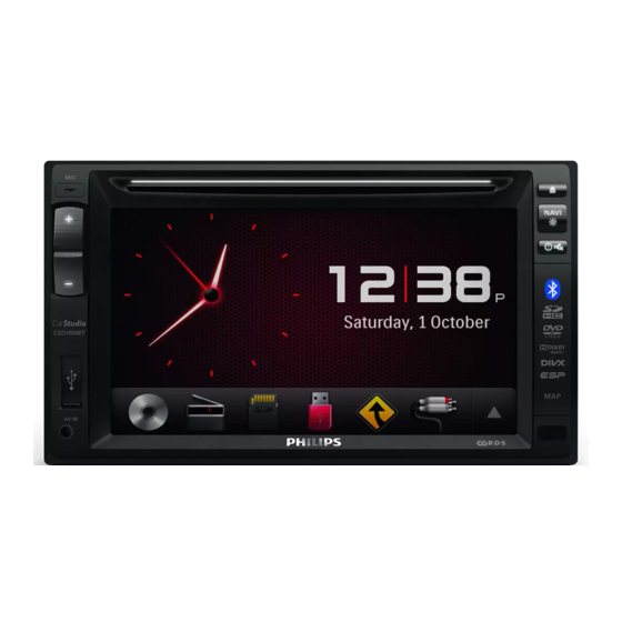
Table of Contents
Advertisement
Quick Links
DISMANTLING INSTRUCTIONS.................................................2
BLOCK DIAGRAM........................................................................3
WIRING DIAGRAM.....................................................................4
CIRCUIT DIAGRAM MAIN BOARD.........................................5-8
CIRCUIT DIAGRAM SERVO BOARD........................................9
CIRCUIT DIAGRAM PANEL BOARD.......................................10-11
CIRCUIT DIAGRAM REMOTE BOARD......................................12
314178538060
MAIN PCB COMPONENT LAYOUT.......................................13-14
SERVO PCB COMPONENT LAYOUT.....................................15-16
PANEL PCB COMPONENT LAYOUT.......................................17-18
REMOTE PCB COMPONENT LAYOUT....................................19-20
SET EXPLODER VIEW DRAWING...........................................21
TROUBLE SHOOTING............................................................22-23
CED1900BT/98
Advertisement
Table of Contents

Summary of Contents for Philips CED1900BT/98
-
Page 1: Table Of Contents
CED1900BT/98 DISMANTLING INSTRUCTIONS..........2 MAIN PCB COMPONENT LAYOUT........13-14 BLOCK DIAGRAM................3 SERVO PCB COMPONENT LAYOUT........15-16 WIRING DIAGRAM..............4 PANEL PCB COMPONENT LAYOUT........17-18 CIRCUIT DIAGRAM MAIN BOARD.........5-8 REMOTE PCB COMPONENT LAYOUT........19-20 CIRCUIT DIAGRAM SERVO BOARD........9 SET EXPLODER VIEW DRAWING...........21 CIRCUIT DIAGRAM PANEL BOARD........10-11 TROUBLE SHOOTING............22-23 CIRCUIT DIAGRAM REMOTE BOARD........12... -
Page 2: Dismantling Instructions
1. Remove the top cover of the main unit, remove the four screws in A,B,C,D position; Uplift the deck mechanism and remove the FFC and remove the deck mechanism 2. Remove the four screws in the L/R side of the bottom cover in E,F,G,H position then remove the bottom cover... -
Page 3: Block Diagram
CED1900 Block Diagram --S3C2451 Solution Subwoofer USB Host 4052 IPHONE output 2.5v Front Rear Chudong Deck (SUNPLUS SPHE8202 Audio output Sanyo 860 2.5V Power Amplifier 16 Pin 7419 7313 SDRAM Flash ST TDA7388 Connector 6.2” Front PanelTFT (800x480) With TCON Radio Tuner SI474X SPI 1... -
Page 4: Wiring Diagram
Wiring Diagram... -
Page 5: Circuit Diagram Main Board
CIRCUIT DIAGRAM -MAIN BOARD... -
Page 9: Circuit Diagram Servo Board
CIRCUIT DIAGRAM -SERVO BOARD... -
Page 10: Circuit Diagram Panel Board
CIRCUIT DIAGRAM -PANEL BOARD... -
Page 12: Circuit Diagram Remote Board
CIRCUIT DIAGRAM -REMOTE BOARD... -
Page 13: Main Pcb Component Layout
PCB LAYOUT-MAIN BOARD TOP SIDE VIEW... - Page 14 PCB LAYOUT-MAIN BOARD BOTTOM SIDE VIEW...
-
Page 15: Servo Pcb Component Layout
PCB LAYOUT-SERVO BOARD TOP SIDE VIEW... - Page 16 PCB LAYOUT-SERVO BOARD BOTTOM SIDE VIEW...
-
Page 17: Panel Pcb Component Layout
PCB LAYOUT-PANEL BOARD TOP SIDE VIEW... - Page 18 PCB LAYOUT-PANEL BOARD BOTTOM SIDE VIEW...
-
Page 19: Remote Pcb Component Layout
PCB LAYOUT-REMOTE BOARD TOP SIDE VIEW... - Page 20 PCB LAYOUT-REMOTE BOARD BOTTOM SIDE VIEW...
-
Page 21: Set Exploder View Drawing
SET EXPLODER VIEW DRAWING... -
Page 22: Trouble Shooting
Product Model Tate 2012-3-27 CED1900BT failure failure cause remark phenomena a To check whether the CN2(ISO) connector of the tail of the unit is connect well . Whether it is loose of the 15A fuse of the CN2(ISO) connector, or insert non in place. b To check the 45 Pin connectors of the CN1 and CN5 whether the socket of it is loose. - Page 23 To check whether the strength of then input signal of the tuner is too weak. Radio abnormal c To check the voltage of the 13 pin of the U8 of the tuner IC, should be +3V3. d.To check the oscillation frequence of crystal X3 of the tuner IC,shuold be 32.768MHz. a.


Need help?
Do you have a question about the CED1900BT/98 and is the answer not in the manual?
Questions and answers