Table of Contents
Advertisement
Quick Links
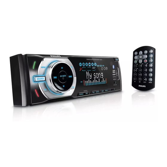
Bluetooth Car entertainment system
CONTENTS
Technical specification ..................................................................1-2
Service measurement setup..........................................................1-3
Service aids .................................................................................1-4
Instructions on CD playability ...............................................2-1.. 2-2
Block diagram ................................................................................3-1
Wiring diagram ..............................................................................4-1
Main board
Circuit diagram ..................................................................5-1..5-5
Layout diagram..................................................................5-6..5-7
Panel board
Circuit diagram .........................................................................6-1
Layout diagram..................................................................6-2..6-3
Servo board
Circuit diagram...................................................................7-1..7-2
Layout diagram .........................................................................7-3
Exploded view diagram .................................................................8-1
Revision list ...................................................................................9-1
©
Copyright 2010 Philips Consumer Electronics B.V. Eindhoven, The Netherlands
All rights reserved. No part of this publication may be reproduced, stored in a retrieval
system or transmitted, in any form or by any means, electronic, mechanical, photocopying,
or otherwise without the prior permission of Philips.
Published by LX 1036 Service Audio
Version 1.1
Subject to modification
CEM5000
/00/55/51
CEM5000X
3141 785 35011
/78
Advertisement
Table of Contents

Related Manuals for Philips CEM5000/00


Summary of Contents for Philips CEM5000/00
-
Page 1: Table Of Contents
Revision list ...................9-1 © Copyright 2010 Philips Consumer Electronics B.V. Eindhoven, The Netherlands All rights reserved. No part of this publication may be reproduced, stored in a retrieval system or transmitted, in any form or by any means, electronic, mechanical, photocopying, or otherwise without the prior permission of Philips. -
Page 2: Technical Specification
1 - 2 TECHNICAL SPECIFICATION Radio Power supply 12 V DC (10.8 V Frequency 87.5 - 108.0 MHz (Europe) - 15.8 V), nega ve range - FM 87.5 - 107.9 MHz ground (American) Fuse 15 A Frequency 522 - 1620 KHz (Europe) range - 530 - 1710 HKz (American) Suitable speaker... - Page 3 MEASUREMENT SETUP Tuner FM Bandpass LF Voltmeter 250Hz-15kHz e.g. PM2534 e.g. 7122 707 48001 RF Generator e.g. PM5326 S/N and distortion meter e.g. Sound Technology ST1700B Use a bandpass filter to eliminate hum (50Hz, 100Hz) and disturbance from the pilottone (19kHz, 38kHz). Tuner AM (MW,LW) Bandpass LF Voltmeter...
-
Page 4: Service Aids
SERVICE AIDS WARNING All ICs and many other semi-conductors are susceptible to electrostatic discharges (ESD). Careless handling during repair can reduce life drastically. When repairing, make sure that you are connected with the same potential as the mass of the set via a wrist wrap with resistance. Keep components and tools also at this potential. -
Page 5: Instructions On Cd Playability
2 - 1 INSTRUCTIONS ON CD PLAYABILITY Customer complaint "CD related problem" Set remains closed! check playability playability ok ? For flap loaders (= access to CD drive possible) "fast" lens cleaning cleaning method is recommended check playability playability ok ? Play a CD for at least 10 minutes check playability... - Page 6 2 - 2 INSTRUCTIONS ON CD PLAYABILITY PLAYABILITY CHECK LIQUID LENS CLEANING Before touching the lens it is advised to clean the surface of the lens by blowing clean air over it. For sets which are compatible with CD-RW discs This to avoid that little particles make scratches on use CD-RW Printed Audio Disc ....7104 099 96611 the lens.
-
Page 7: Block Diagram
3 - 1 3 - 1 SET BLOCK DIAGRAM... -
Page 8: Wiring Diagram
4 - 1 4- 1 SET WIRING DIAGRAM... - Page 9 5 - 1 5 - 1 CIRCUIT DIAGRAM - MAIN BOARD PART 1...
- Page 10 5 - 2 5 - 2 CIRCUIT DIAGRAM - MAIN BOARD PART 2...
- Page 11 5 - 3 5 - 3 CIRCUIT DIAGRAM - MAIN BOARD PART 3...
- Page 12 5 - 4 5 - 4 CIRCUIT DIAGRAM - MAIN BOARD PART 4...
- Page 13 5 - 5 5 - 5 CIRCUIT DIAGRAM - MAIN BOARD PART 5...
- Page 14 5 - 6 5 - 6 LAYOUT DIAGARM - MAIN BOARD TOP SIDE VIEW...
- Page 15 5 - 7 5 - 7 LAYOUT DIAGARM - MAIN BOARD BOTTOM SIDE VIEW...
- Page 16 6 - 1 6 - 1 CIRCUIT DIAGARM - PANEL BOARD RED+8V LCD-59P1 R963 NC LCD-59P BLUE+8V RED+8V R964 2SD1132 Q901 BLUE+8V R935 2SD1132 LED7 LED9 Q903 LED3 LED6 LED13 LED1 LED2 LED17 LED18 LED19 LED15 R938 R939 RED+8V BLUE+8V 9014C R937 Q904...
- Page 17 6 - 2 6 - 2 LAYOUT DIAGRAM - PANEL BOARD...
-
Page 18: Circuit Diagram
7 - 1 7 - 1 CIRCUIT DIAGRAM - SERVO BOARD PART 1... - Page 19 7 - 2 7 - 2 CIRCUIT DIAGRAM - SERVO BOARD PART 2...
-
Page 20: Layout Diagram
7 - 3 7 - 3 LAYOUT DIAGRAM - SERVO BOARD TOP SIDE VIEW... -
Page 21: Layout Diagram
7 - 4 7 - 4 LAYOUT DIAGRAM - SERVO BOARD BOTTOM SIDE VIEW... -
Page 22: Revision List
9 - 1 Revision list Version1.0 ( 3141 785 35010) *Initial Release Version1.1 ( 3141 785 35011) *new -/51 added. - Page 23 TENTATIVE Version No.18052009 LV47002P Development Specification Proposal (BTL 4 channel Car Audio Power Amplifier) The LV47002P is the IC for 4-channel BTL power amplifier that is developed for car audio system. Pch DMOS in the upper side of the output stage and Nch DMOS in the lower side of the output stage are complimentary.
- Page 24 TENTATIVE 4. Maximum Ratings at Ta = 25℃ ℃ ℃ ℃ Parameter Symbol Conditions Ratings Unit Maximum supply Voltage Vcc max 1 No signal, t=1 minute Vcc max 2 During operations Maximum output current Io peak Per channel 4.5/ch Allowable Power dissipation Pd max With an infinity heat sink ℃...
- Page 25 TENTATIVE 7. LV47002P Test and Application circuit rotective circ it i le ilter circ it Lo Level rotective circ it itch The components and constant values within the test circuit are used for confirmation of characteristics and are not guarantees that incorrect or trouble will not occur in application equipment. Note : Information in this document is subject to change without notice.
- Page 26 TENTATIVE 8. Explanation for the functions 1. Standby switch function (pin 4) Threshold voltage of the pin 4 is set by about 2VBE. The amplifier is turned on by the applied voltage of 2.5V or more. Also, the amplifier is turned off by the applied voltage of 0.5V or less.
- Page 27 TENTATIVE 4. Self-diagnosis function (pin 25) By detecting the unusual state of the IC, the signal is output to the pin 25. Also, by controlling the standby switch after the signal of the pin 25 is detected by the microcomputer, the burnout of the speaker can be prevented.
- Page 28 TENTATIVE Icco - Vcc - Vcc RL=Open RL=Open R =0Ω R =0Ω Vcc (V) Vcc (V) Po - Vcc(THD=10%) Po - f(THD=1%) f=1kHz RL=4Ω THD=10% all channel is similar all channel is similar Vcc=14.4V RL=4Ω THD=1% 1000 10000 100000 Vcc (V) f (Hz) THD - Po(f=1kHz) THD - Po(f=100Hz)
- Page 29 TENTATIVE f-Response - Rg Vcc=14.4V RL=4Ω all channel is similar Vcc=14.4V RL=4Ω Vo=0dBm 1000 10000 100000 1000 10000 100000 f (Hz) Rg ( CH.Sep - f(CH1→ → → → ) CH.Sep - f(CH2→ → → → ) ch2→ch1 Vcc=14.4V ch1→ch2 Vcc=14.4V RL=4Ω...
- Page 30 TENTATIVE Offset DIAG - Vcc Pd - Po RL=4Ω f=1kHz R =0Ω RL=4Ω Pd=Vcc×Icc-Po×4ch Detection Level Vcc=14.4V Vcc=16V Vcc (V) Po (W) Mute ATT - V Mute Icco - Vst Vcc=14.4V RL=Open R =0Ω Vcc=14.4V RL=4Ω Vo=20dBm V Mute(V) Vst (V) Note : Information in this document is subject to change without notice.
- Page 32 TDA7419 3 BAND CAR AUDIO PROCESSOR PRELIMINARY DATA FEATURES Figure 1. Package 4 STEREO INPUTS ■ SOFT STEP VOLUME ■ BASS, MIDDLE, TREBLE AND LOUDNESS ■ DIRECT MUTE AND SOFTMUTE ■ SO-28 FOUR INDEPENDENT SPEAKER OUTPUTS ■ SUB WOOFER OUTPUT ■...
- Page 33 TDA7419 Table 2. Supply Symbol Parameter Test Condition Min. Typ. Max. Unit Supply Voltage 10.5 Supply Current = 8.5V SVRR Ripple Rejection @ 1KHz Audioprocessor(all Filters flat) Table 3. Thermal Data Symbol Parameter Value Unit Thermal Resistance Junction-pins max °C/W Th j-pins Table 4.
- Page 34 TDA7419 Table 5. Pin Description Pin Name Function ACOUTR / AC2OUTR AC coupling right output / DSO filter AC2OUT right channel ACINR / FILOR AC coupling right input / DSO filter FILO right channel ACINL / FILOL AC coupling left input / DSO filter FILO left channel ACOUTL / AC2OUTL AC coupling left output / DSO filter AC2OUT left channel SE3L / ACINL...
- Page 35 TDA7419 Audio Processor Features: Input Multiplexer QD / SE: quasi-differential stereo inputs, with selectable single-ended mode SE1: stereo single-ended input SE2: stereo single-ended input SE3 / AC2IN: stereo single-ended input / DSO filter input In-Gain 0 to 15dB, 1dB steps internal offset-cancellation (AutoZero) separate second source-selector Mixing stage...
- Page 36 TDA7419 ELECTRICAL CHARACTERISTICS Table 6. Electrical Characteristcs = 8.5V; T = 25°C; R = 10kΩ ; all gains = 0dB; f = 1kHz; unless otherwise specified Symbol Parameter Test Condition Min. Typ. Max. Unit INPUT SELECTOR Input Resistance All single ended inputs kΩ...
- Page 37 TDA7419 Table 6. Electrical Characteristcs (continued) = 8.5V; T = 25°C; R = 10kΩ ; all gains = 0dB; f = 1kHz; unless otherwise specified Symbol Parameter Test Condition Min. Typ. Max. Unit Delay Time 0.48 0.96 Low Threshold for SM Pin TH Low High Threshold for SM Pin TH High...
- Page 38 TDA7419 Table 6. Electrical Characteristcs (continued) = 8.5V; T = 25°C; R = 10kΩ ; all gains = 0dB; f = 1kHz; unless otherwise specified Symbol Parameter Test Condition Min. Typ. Max. Unit Max Attenuation Step Resolution STEP Mute Attenuation MUTE Attenuation Set Error DC Steps...
- Page 39 TDA7419 Table 6. Electrical Characteristcs (continued) = 8.5V; T = 25°C; R = 10kΩ ; all gains = 0dB; f = 1kHz; unless otherwise specified Symbol Parameter Test Condition Min. Typ. Max. Unit GENERAL µV Output Noise BW=20Hz to 20 kHz all gain = µV BW=20Hz to 20 kHz Output muted...
- Page 40 TDA7419 AutoZero The AutoZero allows a reduction of the number of pins as well as external components by canceling any offset generated by or before the In-Gain-stage (Please notice that externally generated offsets, e.g. gen- erated through the leakage current of the coupling capacitors, are not canceled). The auto-zeroing is started every time the input source is changed and needs max.
- Page 41 TDA7419 5.3.2 Peakr Frequency Figure 6 shows the three possible peak-frequencies 400Hz , 800Hz and 2.4kHz. Figure 6. Loudness Center frequencies @ Attn. = 15dB 1 0 K 1 0 0 5.3.3 Low & High Frequency Boost Figure 7 shows the different Loudness-shapes in low & high frequency boost. Figure 7.
- Page 42 TDA7419 5.3.4 Flat Mode In flat mode the loudness stage works as a 0dB to -15dB attenuator. SoftMute The digitally controlled SoftMute stage allows muting/demuting the signal with a I C-bus programmable slope. The mute process can either be activated by the SoftMute pin or by the I C-bus.
- Page 43 TDA7419 Bass There are four parameters programmable in the bass stage: 5.6.1 Attenuation Figure 9 shows the attenuation as a function of frequency at a center frequency of 80Hz. Figure 10. Bass Control @ f = 80Hz, Q = 1 15.0 10.0 -5.0...
- Page 44 TDA7419 5.6.3 Quality Factors Figure 12 shows the four possible quality factors 1, 1.25, 1.5 and 2. Figure 12. Bass Quality factors @ Gain = 14dB, f = 80Hz 15.0 12.5 10.0 10.0 100.0 1.0K 10.0K 5.6.4 DC Mode It is used for cut only for shelving filter. In this mode the DC-gain is increased by 4.4dB. Inaddition the pro- grammed center frequency and quality factor is decreased by 25% which can be used to reach alternative cen- ter frequencies or quality factors.
- Page 45 TDA7419 Middle There are three parameters programmable in the middle stage: 5.7.1 Attenuation Figure 14 shows the attenuation as a function of frequency at a center frequency of 1kHz. Figure 14. Middle Control @ f = 1 kHz, Q = 1 5.7.2 Center Frequency Figure 14 shows the four possible center frequencies 500Hz, 1kHz, 1.5kHz and 2.5kHz.
- Page 46 TDA7419 5.7.3 Quality Factors Figure 16 shows the four possible quality factors 0.5, 0.75, 1 and 1.25. Figure 16. Middle Quality factors @ Gain = 14dB, fc = 1kHz Treble There are two parameters programmable in the treble stage: 5.8.1 Attenuation Figure 16 shows the attenuation as a function of frequency at a center frequency of 17.5kHz.
- Page 47 TDA7419 5.8.2 Center Frequency Figure 18 shows the four possible center frequencies 10k, 12.5k, 15k and 17.5kHz. Figure 18. Treble Center Frequencies @ Gain = 15dB 1 0 K 1 0 0 Subwoofer Filter The subwoofer lowpass filter has butterworth characteristics with programmable cut-off frequency (80/ 120/160Hz) Figure 19.
- Page 48 TDA7419 5.10 Spectrum Analyzer A fully integrated seven-band spectrum analyzer with programmable quality factor is present. The spec- trum analyzer consists of seven band pass filters with rectifier and sample capacitor that stores the max- imum peak signal level since the last read cycle. This peak signal level can be read by a microprocessor at the SAout-pin.
- Page 49 TDA7419 5.11 AC-Coupling In some applications additional signal manipulations are desired, such as additional band equalizations. For this purpose, an AC-Coupling can be placed before the loudness attenuator or speaker-attenuators, which can be activated or internally shorted by I C-Bus. In short condition, the input-signal of the speaker- attenuator is available at the AC-Outputs.
- Page 50 TDA7419 5.13 Output Selector and Mixing The output-selector allows the front and rear speakers to connect to different sources. The setup of the output selector is shown in Figure 24. A Mixing-stage is placed after the front speaker-attenuator and can be set to mixing-mode.
- Page 51 TDA7419 C BUS SPECIFICATION Interface Protocol The interface protocol comprises: – a start condition (S) – a chip address byte (the LSB determines read/write transmission) – a subaddress byte – a sequence of data (N-bytes + acknowledge) – a stop condition (P) –...
- Page 52 TDA7419 Subaddress (receive mode) Table 7. Subaddress (receive mode) FUNCTION Testing Mode Auto Zero Remain Auto Increment Mode Main Source Selector Main Loudness Soft Mute / Clock Generator Volume Treble Middle Bass Second Source Selector Subwoofer / Middle / Bass Mixing / Gain Effect Speaker Attenuator Left Front Speaker Attenuator Right Front...
- Page 53 TDA7419 Data Byte Specification Table 8. Main Selector (0) FUNCTION Source Selector QD/SE: QD QD/SE: SE mute mute Input Gain 14dB 15dB Auto Zero Table 9. Main Loudness (1) FUNCTION Attenuation -1dB -14dB -15dB Center Frequency Flat 400Hz 800Hz 2400Hz High Boost Loudness Soft Step 22/30...
- Page 54 TDA7419 Table 10. Soft Mute / Clock Generator (2) FUNCTION Soft Mute Pin Influence for Mute Pin and IIC Soft Mute Time 0.48ms 0.96ms 123ms Soft Step Time 0.160ms 0.321ms 0. 642ms 1.28ms 2.56ms 5.12ms 10.24ms 20.48ms Clock Fast Mode Table 11.
- Page 55 TDA7419 Table 12. Treble Filter (4) FUNCTION Gain/Attenuation -15dB -14dB -1dB +1dB +14dB +15dB Treble Center Frequency 10.0kHz 12.5kHz 15.0kHz 17.5kHz Reference Output Select External Vref (4V) Internal Vref (3.3V) Table 13. Middle Filter (5) FUNCTION Gain/Attenuation -15dB -14dB -1dB +1dB +14dB +15dB...
- Page 56 TDA7419 Table 14. Bass Filter (6) FUNCTION Gain/Attenuation -15dB -14dB -1dB +1dB +14dB +15dB Bass Q Factor 1.25 Bass Soft Step Table 15. Second Source Selector (7) FUNCTION Source Selector QD/SE: QD QD/SE: SE mute mute Input Gain 14dB 15dB Rear Speaker Source main source second source...
- Page 57 TDA7419 Table 16. Subwoofer /Middle / Bass (8) FUNCTION Subwoofer Cut-off Frequency flat 80Hz 120Hz 160Hz Middle Center Frequency 500Hz 1000Hz 1500Hz 2500Hz Bass Center Frequency 60Hz 80Hz 100Hz 200Hz Bass DC Mode Smoothing Filter off (bypass) Table 17. Mixing / Gain Effect (9) FUNCTION Mixing to Left Front Speaker Mixing to Right Front Speaker...
- Page 58 TDA7419 Table 18. Spectrum Analyzer / Clock Source / AC Mode (16) FUNCTION Spectrum Analyzer Filter Q Factor 1.75 Reset Mode Auto Spectrum Analyzer Source Bass InGain Spectrum Analyzer Run Reset Clock Source internal external Coupling Mode DC Coupling (without DSO) AC coupling after InGain DC Coupling (with DSO) AC coupling after Bass...
- Page 59 TDA7419 Figure 26. SO-28 Mechanical Data & Package Dimensions inch OUTLINE AND DIM. MECHANICAL DATA MIN. TYP. MAX. MIN. TYP. MAX. 2.65 0.104 0.004 0.012 0.35 0.49 0.014 0.019 0.23 0.32 0.009 0.013 0.020 45° (typ.) 17.7 18.1 0.697 0.713 10.65 0.394 0.419...
- Page 60 TDA7419 Table 20. Revision History Date Revision Description of Changes November 2004 First Issue 29/30...
- Page 61 TDA7419 Information furnished is believed to be accurate and reliable. However, STMicroelectronics assumes no responsibility for the consequences of use of such information nor for any infringement of patents or other rights of third parties which may result from its use. No license is granted by implication or otherwise under any patent or patent rights of STMicroelectronics.
- Page 62 TDA7703/TDA7703R Highly Integrated Tuner for AM/FM-Carradio TARGET DESIGN SPECIFICATION MAIN FEATURES FULLY INTEGRATED VCO FOR WORLD TUNING HIGH PERFORMANCE PLL FOR FAST RDS SYSTEM AM/FM MIXERS WITH HIGH IMAGE REJECTION LQFP44 INTEGRATED AM-LNA AND AM-PINDIODE AUTOMATIC SELF ALIGNMENT FOR IMAGE REJECTION INTEGRATED IF-FILTERS WITH HIGH SELECTIVITY, DYNAMIC RANGE AND ADAPTIVE BANDWIDTH CONTROL DIGITAL IF SIGNAL PROCESSING WITH HIGH PERFORMANCE AND FREE OF...
- Page 63 decoder with group block 1.0 DESCRIPTION synchronization. TDA7703/TDA7703R, a.k.a. HIT44, belong to the HIT (Highly Integrated Tuner) The utilization of digital signal processing family, a new generation of high performance results in numerous advantages against tuners for carradio applications. today’s tuners: •...
- Page 64 TDA7703/TDA7703R 3.0 PINOUT Figure 2 4.0 PIN ASSIGNMENT Pin No. Pin Name Description PLL loopfilter output TCAGCFM FM AGC time constant FMMIXDEC FM mixer decoupling FMIXIN FM mixer input GND-RF RF Ground FMPINDRV FM AGC PIN diode driver VCC-RF 5V supply for RF section TCAM AM AGC time constant PINDDEC...
- Page 65 TDA7703/TDA7703R AMMIXIN AM mixer input VREF165 1.65V reference voltage decoupling VREFDEC 3.3V reference voltage decoupling GND-DIG Digital GND VCC-DIG 5V supply for digital logic VCCREG1V2 VCC of 1.2V regulator REG1V2 1.2V regulator output VDD-3V3 3.3V VDD output / decoupling C bus data C bus clock VDD-1V2 1.2V DSP supply...
- Page 66 TDA7703/TDA7703R 5.0 FUNCTION DESCRIPTION 5.1 FM-Mixer The IMR mixer is optimized for optimum performance in case of a passive tuned prestage and for a passive fixed bandpass without tuning for low-cost application. The input frequency is downconverted to low IF with high image rejection. 5.2 FM - AGC The programmable RFAGC senses the mixer input, the IFAGC senses the IFADC input to avoid overload.
- Page 67 TDA7703/TDA7703R 5.12 I C ADDRESS SELECTION / RDS INTERRUPT INTERFACE PIN As explained also in 5.13.1, there is one pin (RDSINT, pin 29) dedicated to selecting the I address of the device. In the TDA7703R only this pin serves the additional function of RDS interrupt output to communicate to the uP when a new RDS block is available.
- Page 68 TDA7703/TDA7703R a chip address byte must be sent at the beginning of the transmission. The value can be C2 or C8 (according to the mode chosen at start-up during boot) for “write”; as many data bytes as one wants can follow the address before the communication is terminated. See the next section for details on the frame format;...
- Page 69 TDA7703/TDA7703R 6.0 ELECTRICAL CHARACTERISTICS 6.1 ABSOLUTE MAXIMUM RATINGS Limits Symbol Parameter Test Condition, Comments Units Abs. Supply Voltage Storage Temperature °C 6.2 THERMAL DATA Symbol Parameter Test Condition, Comments Value Units LQFP44 10x10, double-layer Thermal Resistance LQFP44 10x10, single-layer Thermal Resistance 6.3 GENERAL KEY PARAMETERS Limits Symbol...
- Page 70 TDA7703/TDA7703R 6.4 FM - SECTION VCC = 4.7V to 5.25V; Tamb = 27°C; f = 76 to 108 MHz; 60dBμV antenna level; mono signal, unless otherwise specified. Antenna level equivalence: 0dBμV = 1μV ref. deviation = 40 kHz rms, table to be inserted > <...
- Page 71 TDA7703/TDA7703R and 39 must be kept in order to latch the correct boot mode (serial bus configuration) Rev. 1.0 10/22...
- Page 72 TDA7703/TDA7703R 6.12.1 I C interface The following parameters apply to the serial bus communication when I C protocol has been selected at start-up. For the other electrical characteristics of the pins, section 6.9 applies. The parameters of the following table are defined as in Figure 1. Limits Symbol Parameter...
- Page 73 TDA7703/TDA7703R 7.0 Overall system performance 7.1 FM overall system performance Antenna level equivalence: 0dBμV = 1μV (Antenna terminal voltage with 50Ω source); no antenna dummy Reference deviation = 40 kHz, de-emphasis = 50 us, f = 1 KHz, V = 60 dBu audio Unless otherwise specified.
- Page 74 TDA7703/TDA7703R 7.2 AM MW overall system performance Antenna level equivalence: 0dBμV = 1μV Level referred to SG output before antenna dummy; capacitive dummy 15pF+65pF Reference modulation = 30%, f =400Hz, F =999kHz (1000 kHz for US), V = 74 dBu audio Unless otherwise specified Limits...
- Page 75 TDA7703/TDA7703R 7.3 AM LW overall system performance Antenna level equivalence: 0dBμV = 1μV before antenna dummy; capacitive dummy 15pF+65pF Reference modulation = 30%, f =400Hz, F =216kHz, V = 74 dBu audio Unless otherwise specified Limits Symbol Parameter Test Condition, Comments Units Tuning range LW (can be modified by the user)
- Page 76 TDA7703/TDA7703R 8.0 FRONT-END PROCESSING All the parameters in this section refer to the programmability of the FE part of the device (registers). The part of the registers that are not described here have either fixed values (shown in the tables with a black background) or values written by the tuner drivers, and therefore not directly by the user (shown in the tables with a red background, if the registers are written exclusively by the tuner drivers, and with orange background if they can be written by the user for the manual FE alignment operation).
- Page 77 TDA7703/TDA7703R 9.0 WEAK SIGNAL PROCESSING All the parameters in this section refer to the programmability of the DSP part of the device. The typical values are those set by default parameters (start-up without parametric change from main uP); the max and the min values refer to the programmability range. The values are referred to the typical application.
- Page 78 TDA7703/TDA7703R 9.1.3 Stereo blend (continuous set) Range Symbol Parameter Test Condition, Comments Units field strength = 80 dBu, pilot MaxSep Maximum stereo separation deviation = 6.75 kHz separation = MaxSep - 1 dB SBFSsp Start point vs. field strength no multipath present separation = 1 dB SBFSep End point vs.
- Page 79 TDA7703/TDA7703R 9.1.4 High cut control (continuous set) Range Symbol Parameter Test Condition, Comments Units minimum RF level for widest HCFSsp Start point vs. field strength HC filter (filter # 7) no multipath present maximum RF level for HCFSep End point vs. field strength narrowest HC filter (filter # 0) no multipath present Field strength-related...
- Page 80 TDA7703/TDA7703R 9.2 AM IF-processing 9.1.1 Channel selection filter Range Symbol Parameter Test Condition, Comments Units CSF BW Channel selection filter BW response: - 3dB ±3.7 9.2.1 Soft mute (continuous set) Range Symbol Parameter Test Condition, Comments Units audio atten = 1 dB SMsp Start point vs.
- Page 81 TDA7703/TDA7703R 10.0 APPLICATION SCHEMATIC Figure 5 (FM Eu/US/JP, AM LW/MW application) Rev. 1.0 20/22...
- Page 82 TDA7703/TDA7703R 11 PACKAGE INFORMATION Rev. 1.0 21/22...
- Page 83 TDA7703/TDA7703R Information furnished is believed to be accurate and reliable. However, STMicroelectronics assumes no responsibility for the consequences of use of such information nor for any infringement of patents or other rights of third parties which may result from its use. No license is granted by implication or otherwise under any patent or patent rights of STMicroelectronics. Specifications mentioned in this publication are subject to change without notice.