Table of Contents
Advertisement
RX-V100D
This manual has been provided for the use of authorized YAMAHA Retailers and their service personnel.
It has been assumed that basic service procedures inherent to the industry, and more specifically YAMAHA Products, are already
known and understood by the users, and have therefore not been restated.
WARNING:
IMPORTANT:
The data provided is believed to be accurate and applicable to the unit(s) indicated on the cover. The research, engineering, and
service departments of YAMAHA are continually striving to improve YAMAHA products. Modifications are, therefore, inevitable
and specifications are subject to change without notice or obligation to retrofit. Should any discrepancy appear to exist, please
contact the distributor's Service Division.
WARNING:
IMPORTANT:
I CONTENTS
TO SERVICE PERSONNEL .......................................... 2
FRONT PANEL .............................................................. 3
REAR PANELS .............................................................. 3
REMOTE CONTROL PANEL ........................................ 4
SPECIFICATIONS ...................................................... 5~6
ADVANCED SETUP ...................................................... 7
INTERNAL VIEW ........................................................... 7
DISASSEMBLY PROCEDURES ............................. 8~11
SELF DIAGNOSIS FUNCTION (DIAG) ................. 12~30
1 0 0 9 8 6
SERVICE MANUAL
IMPORTANT NOTICE
Failure to follow appropriate service and safety procedures when servicing this product may result in personal
injury, destruction of expensive components, and failure of the product to perform as specified. For these reasons,
we advise all YAMAHA product owners that any service required should be performed by an authorized
YAMAHA Retailer or the appointed service representative.
The presentation or sale of this manual to any individual or firm does not constitute authorization, certification or
recognition of any applicable technical capabilities, or establish a principle-agent relationship of any form.
Static discharges can destroy expensive components. Discharge any static electricity your body may have
accumulated by grounding yourself to the ground buss in the unit (heavy gauge black wires connect to this buss).
Turn the unit OFF during disassembly and part replacement. Recheck all work before you apply power to the unit.
AMP ADJUSTMENT .................................................... 31
IC DATA ................................................................. 32~35
BLOCK DIAGRAM ................................................. 36~37
DISPLAY DATA ........................................................... 38
PRINTED CIRCUIT BOARD .................................. 39~51
PIN CONNECTION DIAGRAM .................................... 52
SCHEMATIC DIAGRAM ........................................ 53~60
PARTS LIST ........................................................... 61~73
REMOTE CONTROL .................................................... 74
2005
All rights reserved.
This manual is copyrighted by YAMAHA and may not be copied or
redistributed either in print or electronically without permission.
AV RECEIVER
P.O.Box 1, Hamamatsu, Japan
'05.11
Advertisement
Table of Contents

Subscribe to Our Youtube Channel
Related Manuals for Yamaha RX-V100D


Summary of Contents for Yamaha RX-V100D
-
Page 1: Table Of Contents
This manual has been provided for the use of authorized YAMAHA Retailers and their service personnel. It has been assumed that basic service procedures inherent to the industry, and more specifically YAMAHA Products, are already known and understood by the users, and have therefore not been restated. -
Page 2: To Service Personnel
RX-V100D I TO SERVICE PERSONNEL 1. Critical Components Information AC LEAKAGE Components having special characteristics are marked s WALL EQUIPMENT TESTER OR and must be replaced with parts having specifications equal OUTLET UNDER TEST EQUIVALENT to those originally installed. 2. Leakage Current Measurement (For 120V Models Only) -
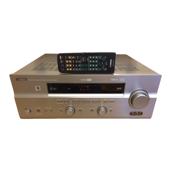
Page 3: Front Panel
RX-V100D I FRONT PANEL B model I REAR PANELS B model G model... -
Page 4: Remote Control Panel
RX-V100D I REMOTE CONTROL PANEL RAV306... -
Page 5: Specifications
..................95 W + 95 W 1 switched outlet Stereo ..................70 dB "SILENT CINEMA" is a trademark of YAMAHA CORPORATION. B model ........100 W max. total / 0.4 A max. total Dynamic Power Per Channel (IHF) Harmonic Distortion (1 kHz) Dimensions (W x H x D) FRONT L/R (8 ohms/6 ohms/4 ohms/2 ohms) .. - Page 6 RX-V100D • Set Menu Table CATEGORY MAIN MENU SUB MENU SELECT MENU VALUE [INITIAL] CATEGORY MAIN MENU SUB MENU SELECT MENU VALUE [INITIAL] 2 INPUT MENU A ) I/O ASSIGN C . V [A] : DVD [DVD] / VCR / V-AUX / DTV/CBL C .
-
Page 7: Advanced Setup
RX-V100D I ADVANCED SETUP • Changing Speaker Impedance • Resetting the factory presets To change the Speaker Impedance, do the following pro- To reset all of parameters, do the following procedure. cedure. This procedure completely resets ALL parameters, in- cluding the SET MENU, level, assign, and tuner presets. -
Page 8: Disassembly Procedures
RX-V100D I DISASSEMBLY PROCEDURES (Remove parts in the order as numbered.) Disconnect the power cable from the AC outlet. 1. Removal of Top Cover a. Remove 4 screws (1), 4 screws (2) and 1 screws (3). (Fig. 1) b. Slide the Top Cover rearward to remove it. (Fig. 1) 2. - Page 9 RX-V100D 5. Removal of DSP P.C.B. a. Remove 1 screw (8). (Fig. 2) b. Remove 7 screws (9). (Fig. 3) c. Remove CB2 and CB11. (Fig. 2) d. Lift up the SUBTRANS (2) P.C.B. and remove the CB1. (Fig. 2) e.
- Page 10 RX-V100D 6. Removal of FUNCTION, SUBTRANS (2), (3), (6), (7), (9), DAB P.C.B.s and Tuner a. Remove CB4, CB5, CB6, CB307, CB351, CB452 and CB453. (Fig. 4) b. Remove 22 screws (0). (Fig. 3) c. Remove FUNCTION, SUBTRANS (2), (3), (4), (6), (7), (9), DAB P.C.B.s and the Tuner. (Fig. 4) SUBTRANS (4) P.C.B.
- Page 11 RX-V100D When checking the P.C.B.: • Put a Cloth over the equipment. Put the MAIN (1), (5), and POWER (1), (2) P.C.B.s together with the heat sink upright on the Cloth and check them. (Fig. 6) • Reconnect all cables (connectors) that have been disconnected.
-
Page 12: Self Diagnosis Function (Diag)
RX-V100D I SELF DIAGNOSIS FUNCTION (DIAG) This unit has self diagnosis functions that are intended for inspection, measurement and location of faulty point. There are 21 DIAG menu items, each of which has sub-menu items. Listed in the table below are menu items and sub-menu items. - Page 13 RX-V100D No DIAG menu sub-menu 14 IF STATUS 1. DST 2. DMD 3. DIF 4. PC 5. CS1 6. CS2 7. DEI 8. BS1 9. BS2 10. BS3 11. BS4 12. BS5 13. BS6 14. BS7 15. BS8 16. MTT 17.
- Page 14 RX-V100D • Starting DIAG Press the “STANDBY/ON” key while simultaneously pressing those two keys of the main unit as indicated in the figure below. Keys of main unit Turn on the power while pressing these keys. • Starting DIAG in the protection cancel mode If the protection function works and causes hindrance to trouble diagnosis, cancel the protection function as described below, and it will be possible to enter the DIAG mode.
- Page 15 RX-V100D • Display provided when DIAG started The FL display of the main unit displays the protection function history data and the version (1 alphabet) and the DIAG menu [sub-menu (ANALOG BYPASS) of DIAG menu No.1 BYPASS] a few seconds later.
- Page 16 RX-V100D When there is a history of protection Version (1 alphabet) function due to abnormal DC output Voltage display in % Cause: DC output of the power amplifier is abnormal. Supplementary information: The abnormal voltage is displayed in % based on 5V as 100%.
- Page 17 RX-V100D • Operation procedure of DIAG menu and SUB-MENU There are 21 MENU items, each of which has some SUB-MENU items. DIAG menu selection Main unit: Select the menu using the PROGRAM knob. SUB-MENU selection Main unit: Select the sub-menu using (Forward) and (Reverse) keys of PRESET/TUNING.
- Page 18 RX-V100D • Details of DIAG menu 1. BYPASS Using the sub-menu, it is possible to select analog bypass output or DSP bypass output. ANALOG BYPASS Reference data INPUT: DVD ANALOG SUBWOOFER OUTPUT: 50 Hz, Others: 1 kHz SPEAKERS OUT SUBWOOFER...
- Page 19 RX-V100D 2. RAM THROUGH Using the sub-menu, it is possible to select margin output or full-bit output. RAM MARGIN Following head margin is reserved. FRONT CENTER SURROUND SURROUND BACK SUBWOOFER +15.0 dB +14.0 dB +9.0 dB +8.0 dB +18.0 dB...
- Page 20 RX-V100D 3. PRO LOGIC Dolby PRO LOGIC is applied to input stereo source. Reference data INPUT: DVD ANALOG SUBWOOFER OUTPUT: 50 Hz, Others: 1 kHz SPEAKERS OUT SUBWOOFER Input level Volume FRONT L/R CENTER SURROUND L/R SURROUND BACK OUTPUT - ∞...
- Page 21 RX-V100D 4. SPEAKERS SET The analog switch settings for each sub-menu are as shown in the table below. Sub-menu FRONT CENTER SUR. SUR.B FRNT: SML 0 dB SMALL LARGE LARGE LARGE SWFR CENTER: NONE LARGE NONE LARGE LARGE SWFR LFE/B: FRNT...
- Page 22 RX-V100D 5. Xch-INPUT The speaker impedance can be selected. XCH INPUT_6 Reference data INPUT: MULTI CH INPUT SUBWOOFER OUTPUT: 50 Hz, Others: 1 kHz SPEAKERS OUT SUBWOOFER Input level Volume FRONT L/R CENTER SURROUND L/R SURROUND BACK OUTPUT - ∞...
- Page 23 RX-V100D 7. VFD CHECK This program is used to check the FL display section. The display condition varies as shown below according to the sub- menu operation. The signals are processed using EFFECT OFF (The L/R signal is output using ANALOG MAIN BYPASS.)
- Page 24 RX-V100D 9. DAB CHECK Using the DIAG menu, it is possible to select DAB SCAN, DLS, SIGNAL QUALITY. DAB SCAN The channel that can be received is searched. When reception is completed the service label is displayed. Scanning ... Display of Service label.
- Page 25 RX-V100D 11. AD DATA CHECK This menu is used to display the A/D conversion value of the terminals which detect panel keys of the main unit and protection functions in % using the sub-menu. During signal processing, the condition before execution is maintained.
- Page 26 RX-V100D 12. V CONV STATUS Not applied to this model. LOW BYTE DATA HIGH BYTE DATA 13. XM STATUS Not applied to this model. 14. IF STATUS (Input function status) Using the sub-menu, the status data is displayed one after another in the hexadecimal notation.
- Page 27 RX-V100D <2nd byte> <3rd byte> <4th byte> Fs information of reproduction signal Audio code mode information of Format information of reproduction signal reproduction signal Display Fs (kHz) Display Audio code Display Signal format Analog Analog 32 kHz 44.1 kHz PCM Audio...
- Page 28 RX-V100D DEI: Decoder information Not applied to this model. BS1-8: Bit stream information Not applied to this model. MTT: Mute Trigger Not applied to this model. DGI: Digital information Not applied to this model. 15. DSP BUS CHECK This menu is used to self-diagnose whether or not the bus connection for the TI (DA60Y) and the external ROM/RAM is made properly.
- Page 29 RX-V100D 19. SOFT SW Note) Changing the function setting may hinder the proper operation. This menu is used to switch the function settings on P.C.B. through the software so as to activate the product. The protection function follows the P.C.B. settings. When connected to AC or in the maker preset state, the unit is initialized to the P.C.
- Page 30 RX-V100D 20. SOFTWARE VERSION The version, checksum and the port specified by the microprocessor are displayed. The signal is processed using EFFECT OFF. The checksum is obtained by adding the data at every 16 bits for each program area and expressing the result as a 4- figure hexadecimal data.
-
Page 31: Amp Adjustment
RX-V100D I AMP ADJUSTMENT Confirmation of Idling Current of MAIN (1) P. C. B. • Right after power is turned on, confirm that each measured voltage across the terminals of R45 (FRONT Lch), R46 (FRONT Rch), R50 (CENTER), R47 (SURROUND Lch), R48 (SURROUND Rch), R49 (SURROUND BACK Rch) is between 0.1 mV and 10.0 mV. -
Page 32: Ic Data
RX-V100D I IC DATA IC5 : D60YA003BPYP225 (DSP P.C.B.) Digital Signal Processors Decoder EMIF32 L2 Cache/ L1P Cache Memory Direct Mapped 4 Banks McASP1 * No replacement part available. 4K Bytes Total 64K Bytes Total McASP0 (4-Way) C67x McBSP1 Instruction Fetch... - Page 33 RX-V100D IC5 : D60YA003BPYP225 (DSP P.C.B.) IC5 : D60YA003BPYP225 (DSP P.C.B.) Decoder Decoder No. Name Function No. Name Function 41 SCL0 I2C0 clock 99 EA17 For external memory, Address 17 42 SDA0 I2C0 data 100 EA19 For external memory, Address 19 43 CVDD 1.2V power supply...
- Page 34 RX-V100D IC5 : D60YA003BPYP225 (DSP P.C.B.) IC451: M30626FHPF (SUBTRANS P.C.B.) Decoder 16-bit Microprocessor No. Name Function 157 CVDD 1.2V power supply 158 VSS Ground 159 AHCLKX1 McASP1 transmission MCLK 160 GP0[8] General purpose I/O0 port 8 161 AHCLKR1 McASP1 reception MCLK 162 DVDD 3.3V power supply...
- Page 35 RX-V100D IC451: M30626FHPFP (SUBTRANS P.C.B.) IC451: M30626FHPFP (SUBTRANS P.C.B.) 16-bit Microprocessor 16-bit Microprocessor Port Name Terminal Name Function Port Name Terminal Name Function PowerOn Pure Direct Standby Sleep PowerOn Pure Direct Standby Sleep DTZ2 P04/D4 INPUT Selector Rotaly A P66/RXD1/SCL1...
- Page 36 RX-V100D I BLOCK DIAGRAM (1/2) LC89057W Selector • See page 53, 54 → SCHEMATIC DIAGRAM SN74LV157APWR IC14 D60YA003BPYP225 Main Decoder AXR1(5) FL/FR MD/CD-R (J model) AXR1(0) IC306 27,28 DAPL/DAPR PL/PR AXR1(3) IC19 DTV/CBL C/SW 25,26 DAC/DASW C/SW AXR1(2) IC21 Buffer...
-
Page 37: Block Diagram
RX-V100D I BLOCK DIAGRAM (2/2) OPERATION (4) POWER / 4ohms RY401 TRANSFORMER • See page 56 → SCHEMATIC DIAGRAM RY126 MAIN (2) V-AUX • See page 57 → SCHEMATIC DIAGRAM Input Selector LA7956 DTV/CBL IC901 RY126 Q903 SUBTRANS (6) SUBTRANS (3) •... -
Page 38: Display Data
RX-V100D G ANODE CONNECTION I DISPLAY DATA 13G~2G G V801 : 17-BT-25GNK (WF784700) PATTERN AREA G PIN CONNECTION Pin No. Connection Pin No. Connection Note : 1) F1, F2 ..Filament 2) NP ..No pin 3) NX ..No extened pin 4) DL .. -
Page 39: Printed Circuit Board
RX-V100D I PRINTED CIRCUIT BOARD • Semiconductor Location Ref. No. Location DIGITAL DIGITAL OUTPUT INPUT OPTICAL DSP P.C.B. (Side A) MD/CD-R MD/CD-R DTV/CBL COAXIAL DSP P.C.B. (Side B) Lead Solder Used Lead Free Solder Used IC10 IC11 IC12 IC13 IC14... - Page 40 RX-V100D I PRINTED CIRCUIT BOARD • Semiconductor Location Ref. No. Location FUNCTION P.C.B. (Side A) D303 (CB2) D304 IC305 OPERATION (5) (CB11) Q307 (W882) SUBTRANS (2) POWER (1) Q308 POWER (1) (CB460) (CB358) (CB351) MULTI CH INPUT FRONT SURROUND SUBWOOFER...
- Page 41 RX-V100D I PRINTED CIRCUIT BOARD • Semiconductor Location Ref. No. Location FUNCTION P.C.B. (Side B) Lead Free Solder Used D301 D302 IC301 IC303 IC304 IC306 Q301 Q302 Q303 Q304 Q305 Q306 Q309 Q310 Q311 Q312 64 65...
- Page 42 RX-V100D I PRINTED CIRCUIT BOARD • Semiconductor Location OPERATION (1) P.C.B. SUBTRANS (2) Ref. No. Location (CB456) (Side A) D803 FL DISPLAY CKFD D804 DTFD CEFD ADKEY1 IC801 ADKEY0 TONEB Q801 TONEA Q802 /BLK /PURD /PSW Q803 Q804 Q805 Q806...
- Page 43 RX-V100D I PRINTED CIRCUIT BOARD • Semiconductor Location Ref. No. Location OPERATION (2) P.C.B. (Side A) OPERATION (5) P.C.B. (Side A) D871 D872 D873 OPERATION (1) FUNCTION D881 (CB803) (CB306) D882 to Power Transformer D883 D884 STANDBY VIDEO AUDIO VIDEO AUX OPERATION (5) P.C.B.
- Page 44 RX-V100D I PRINTED CIRCUIT BOARD Lead Free Solder Used • Semiconductor Location Ref. No. Location Ref. No. Location MAIN (1) P.C.B. (Side A) POWER (1) Q16A POWER (1) POWER (1) (CB353) Q16C (CB352) (CB359) Q18A SUBTRANS (2) Q18C (CB453) POWER (1)
- Page 45 RX-V100D I PRINTED CIRCUIT BOARD Lead Free Solder Used • Semiconductor Location Ref. No. Location MAIN (2) P.C.B. (Side A) D122 SPEAKERS D123 D125 FRONT SURROUND D127 D129 CENTER SURROUND BACK D133 D141 D142 D143 D144 Q120 Q121 Q123 Q124...
- Page 46 RX-V100D I PRINTED CIRCUIT BOARD Lead Free Solder Used • Semiconductor Location POWER (1) P.C.B. (Side A) to Power Transformer Ref. No. Location MAIN (1) MAIN (1) MAIN (1) FUNCTION D301 (W15) (CB6) (CB5) (CB307) D302 D312 D313 FUNCTION IC301...
- Page 47 RX-V100D I PRINTED CIRCUIT BOARD S VIDEO • Semiconductor Location DTV/ Ref. No. Location MONITOR OUT SUBTRANS (1) P.C.B. (Side A) SUBTRANS (3) P.C.B. (Side A) D401 D402 D403 D404 D405 D406 D407 D408 D409 D410 D411 IC401 VSEL MAIN (2)
- Page 48 RX-V100D I PRINTED CIRCUIT BOARD • Semiconductor Location Ref. No. Location SUBTRANS (2) P.C.B. (Side A) SUBTRANS (2) P.C.B. (Side B) Lead Free Solder Used D451 D452 to TUNER D453 MAIN (2) D454 (CB122) D455 D456 D457 D458 D459 IC451...
- Page 49 RX-V100D I PRINTED CIRCUIT BOARD • Semiconductor Location SUBTRANS (4) P.C.B. (Side A) SUBTRANS (6) P.C.B. (Side A) Ref. No. Location IC701 IC702 COMPONENT VIDEO VIDEO IC901 DTV/ MONITOR DTV/ Q701 MONITOR OUT Q901 Q903 Q904 AUX-V +12V VSEL CMP0 CMP1 SUBTRANS (4) P.C.B.
- Page 50 RX-V100D I PRINTED CIRCUIT BOARD SUBTRANS (7) P.C.B. (Side A) SUBTRANS (9) P.C.B. (Side A) AUDIO OUTPUT DTV/ WOOFER SUBTRANS (7) (CB751) FUNCTION (CB301) SUBTRANS (9) (CB442) SUBTRANS (7) P.C.B. (Side B) Lead Free Solder Used...
-
Page 51: Printed Circuit Board
RX-V100D I PRINTED CIRCUIT BOARD • Semiconductor Location DAB P.C.B. (Side A) DSB P.C.B. (Side B) Lead Free Solder Used Ref. No. Location to Power Transformer SUBTRANS (2) (CB454) ICXM DB_SDA DB_SCLK AGND DGND XMMCK XMWCK XMSCK XMSDO DTPWR (W1) -
Page 52: Pin Connection Diagram
RX-V100D I PIN CONNECTION DIAGRAM • ICs • Diodes µPC29M33T-E1-AZ 1N4002S MTZJ15A 1SS355 SB01-05Q LM61CIZ NJU7201L55 NJM7805FA NJM79M05FA PQ012FZ01ZPH NJM2388F 1SS133 MTZJ2.4B MA8030-L Anode NJM7812FA NJM79M12FA 1SS270A MTZJ27A MA8051-M Anode MTZJ30A MA8056-M MA8068-M MA8075-H Cathode MA8091-M Cathode MA8100-M UDZ3.6BTE-17 1: GND... -
Page 53: Schematic Diagram
RX-V100D SCHEMATIC DIAGRAM (DSP 1/2) Page 60 Page 59 to DAB_CB4 to SUBTR (2)_CB457 Point: A-3 Pin 28 of IC2 IC2: LC89057W-VF4D-E Digital Audio Interface Transceiver EMPHA/UO AUDIO/VO XMODE Microcontroller RXOUT Cbit, Ubit BUFFER RERR Input Demodulation Data Selector &... - Page 54 RX-V100D SCHEMATIC DIAGRAM (DSP 2/2) Page 55 Page 55 to FUNCTION_W301 to FUNCTION_CB305 IC9: NJM78M05DL1A Voltage Regulator INPUT OUTPUT COMMON IC14: SN74LV157APWR Quadruple 2-line to 1-line data selectors/multiplexers SELECTOR DIGITAL IN ANALOG IN 11.9 IC16: AK4628VQ 192kHz 24Bit 8-channel CODEC...
- Page 55 RX-V100D SCHEMATIC DIAGRAM (FUNCTION) Page 54 Page 59 Page 54 Page 56 to DSP_CB11 to SUBTR (2)_CB460 to DSP_CB2 to OPERATION (5)_W882 MUTE 10.5 ANALOG IN 11.9 -10.1 -10.7 -10.1 -12.0 FRONT L 11.9 -11.9 -11.9 -12.0 MUTE CENTER ANALOG IN...
- Page 56 RX-V100D SCHEMATIC DIAGRAM (OPERATION) FL DISPLAY AC5.6 to POWER TRANSFORMER POWER SW OPERATION (2) -26.1 -24.4 -26.2 -22.6 -24.2 -26.3 -22.5 -24.4 -28.1 -24.4 -24.3 -22.6 -28.1 -20.7 -24.4 -24.4 -24.3 -26.1 -20.7 -18.9 FL DRIVER -18.9 -22.5 -18.9 -26.3 -17.0...
- Page 57 RX-V100D SCHEMATIC DIAGRAM (MAIN) Page 59 to SUBTR (2)_CB453 53.8 53.8 53.8 53.8 53.8 -1.0 LTS0810-1015FM -0.5 -1.0 -0.5 -0.5 -1.0 -47.2 -53.8 -47.8 -53.8 -47.8 -47.8 53.8 53.8 53.8 -1.0 -0.5 -0.5 -0.5 -1.0 -1.0 -53.8 -53.8 -47.2 FRONT L -47.8...
- Page 58 RX-V100D SCHEMATIC DIAGRAM (POWER) 19.0 AC30.4 -0.1 -0.1 12.0 18.9 10.3 -20.1 10.3 to POWER TRANSFORMER AC18.5 10.3 -0.2 53.3 52.7 -11.9 -12.0 -20.1 FRONT L 52.7 53.8 -0.6 -0.6 Page 57 to MAIN (1)_W8 IC301: LM61CIZ Temperature Sensor 53.3 52.7...
- Page 59 RX-V100D SCHEMATIC DIAGRAM (SUBTRANS) to POWER CABLE to POWER TRANSFORMER AC69.0 -0.2 SUBTR (7) AC6.3 10.3 10.3 SUBTR (1) Page 55 to FUNCTION_CB303 SUBTR (6) INPUT SELECTOR -11.9 11.3 IC402: TC4013BP Dual D-type Flip Flop -11.9 11.9 RESET1 -11.9 SET1...
-
Page 60: Schematic Diagram
RX-V100D SCHEMATIC DIAGRAM (DAB) Page 59 to SUBTR (2)_CB454 Page 53 to DSP_W1 to POWER TRANSFORMER IC1: NJM7805FA IC3: PQ3RD23 Voltage Regulator Low power-loss voltage regulator INPUT Specific IC OUTPUT COMMON # All voltages are measured with a 10MΩ/V DC electronic volt meter. -
Page 61: Parts List
RX-V100D PARTS LIST I ELECTRICAL PARTS I WARNING Components having special characteristics are marked s and must be replaced with parts having specifications equal to those originally installed. ABBREVIATIONS IN THIS LIST ARE AS FOLLOWS: C.A.EL.CHP : CHIP ALUMI.ELECTROLYTIC CAP L.EMIT... - Page 62 RX-V100D P.C.B. DSP P.C.B. DSP Ref. No. Part No. Description Markets Ref. No. Part No. Description Markets WG225200 P.C.B. UR238100 C.EL 100uF V7828500 SOCKET 18P TE TUC SERIES US035100 C.CE.CHP 0.1uF 16V B VQ044800 CN.BS.PIN C84-87 US135100 C.CE.CHP 0.1uF CB11 LB919020 CN.BS.PIN...
- Page 63 RX-V100D P.C.B. DSP P.C.B. DSP & P.C.B. FUNCTION Ref. No. Part No. Description Markets Ref. No. Part No. Description Markets C194-195 UR237100 C.EL 10uF WB001400 CN.PHOT.SN 1P GP1FA553RZ C198-199 UA655100 C.MYLAR 0.1uF 50V J WB001400 CN.PHOT.SN 1P GP1FA553RZ C200-203 UA655100 C.MYLAR 0.1uF...
- Page 64 RX-V100D P.C.B. FUNCTION & P.C.B. OPERATION P.C.B. OPERATION & P.C.B. MAIN Ref. No. Part No. Description Markets Ref. No. Part No. Description Markets D303-304 VV307700 DIODE 1N4002S C826-827 US063100 C.CE.CHP 1000pF 50V B IC301 X5092A00 IC BD3816K1 C871 UA654100 C.MYLAR 0.01uF...
- Page 65 RX-V100D P.C.B. MAIN P.C.B. MAIN Ref. No. Part No. Description Markets Ref. No. Part No. Description Markets UT952150 C.PP 150pF 100V D127 VG442900 DIODE.ZENR MTZJ27B UT952150 C.PP 150pF 100V D129 VG442900 DIODE.ZENR MTZJ27B UR267470 C.EL 47uF s D133 WA653200 DIODE.BRG TS6P03G 6.0A 200V...
- Page 66 RX-V100D P.C.B. MAIN P.C.B. MAIN & P.C.B. POWER Ref. No. Part No. Description Markets Ref. No. Part No. Description Markets s Q262-267 V4096000 TR 2SA1770 S,T R278-283 HV755100 R.CAR.FP 100Ω 1/4W HV754100 R.CAR.FP 10Ω 1/4W R284 VP939700 R.MTL.FLM 4.7Ω HL006270 R.MTL.OXD 2.7KΩ...
- Page 67 RX-V100D P.C.B. POWER & P.C.B. SUBTRANS P.C.B. SUBTRANS Ref. No. Part No. Description Markets Ref. No. Part No. Description Markets C340 UA652100 C.MYLAR 100pF 50V J WG225000 P.C.B. SUBTRANS C341 UA652220 C.MYLAR 220pF 50V J WG225100 P.C.B. SUBTRANS C342-343 UR266100 C.EL...
- Page 68 RX-V100D P.C.B. SUBTRANS P.C.B. SUBTRANS Ref. No. Part No. Description Markets Ref. No. Part No. Description Markets C475-477 UR037470 C.EL 47uF D455-458 VU992600 DIODE.ZENR MA8051-M 5.1V C478 US135100 C.CE.CHP 0.1uF D459 VU993000 DIODE.ZENR MA8056-M 5.6V C479-480 US062330 C.CE.CHP 330pF 50V B...
-
Page 69: Parts List
RX-V100D Parts List for Carbon Resistors P.C.B. SUBTRANS & P.C.B. DAB Chip Resistors The chip resistor is not supplied as a replacement part. Ref. No. Part No. Description Markets * When a chip resistor is necessary, use the following part. - Page 70 RX-V100D I EXPLODED VIEW 7 (1) 7 (4) 200-1 AMP UNIT 7 (7) 7 (3) 7 (6) 7 (9) 7 (2) B model SUB CHASSIS UNIT LEFT RIGHT FRONT PANEL UNIT...
- Page 71 RX-V100D I MECHANICAL PARTS Schm Ref. PART NO. Description Remarks Markets WG225200 P.C.B. ASS'Y WE593600 P.C.B. ASS'Y FUNCTION WG225000 P.C.B. ASS'Y SUBTRANS WG225100 P.C.B. ASS'Y SUBTRANS WG225400 P.C.B. ASS'Y WD048400 AM/FM TUNER FAE485-E01F * s 15 X6960A00 POWER TRANSFORMER s 16...
- Page 72 RX-V100D I EXPLODED VIEW (FRONT PANEL UNIT & SUB CHASSIS UNIT) I MECHANICAL PARTS (FRONT PANEL UNIT & SUB CHASSIS UNIT) Schm 3-114 Ref. PART NO. Description Remarks Markets WF991100 FRONT PANEL 3-114 WF991300 FRONT PANEL WF991400 FRONT PANEL WF991600...
- Page 73 RX-V100D I EXPLODED VIEW (AMP UNIT) I MECHANICAL PARTS (AMP UNIT) Schm Ref. PART NO. Description Remarks Markets 2-104 2-104 WE588300 P.C.B. ASS'Y MAIN WE588800 P.C.B. ASS'Y POWER 2-20 MF117140 FLEXIBLE FLAT CABLE 17P 140mm P=1.25 2-11 VV849300 RADIATION SHEET...
-
Page 74: Remote Control
RX-V100D I REMOTE CONTROL RAV306 G SCHEMATIC DIAGRAM CODE Function CD-R TUNER DVD (P) DVD (Y) DVD (M) DVD-R (P) 0Ω TV POWER – – – – – – – – – AV POWER – – – 7F-80 – A5-AA...
Need help?
Do you have a question about the RX-V100D and is the answer not in the manual?
Questions and answers