Simoco SRM9000 Service Manual

Simoco SRM9000 Service Manual

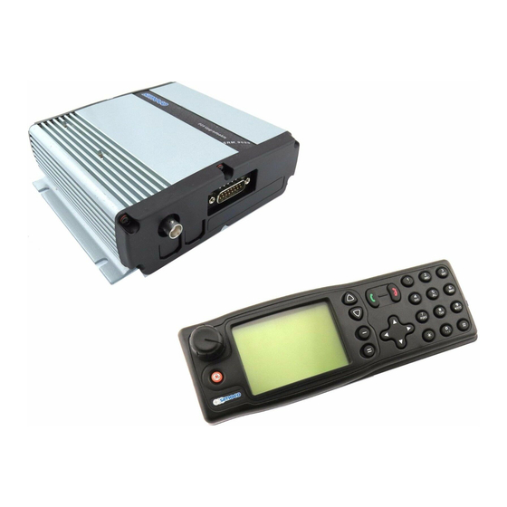
Srm 9000 series fm vhf/uhf mobile radio transceiver
Hide thumbs Also See for SRM9000:
Table of Contents

Advertisement

SRM 9000 Series
FM VHF/UHF Mobile Radio Transceiver
SERVICE MANUAL
TNM-M-E-0001
October 2000
Draft D
abcde
abcde

Advertisement

Table of Contents
loading
Need help?

Need help?

Do you have a question about the SRM9000 and is the answer not in the manual?

Questions and answers

Summary of Contents for Simoco SRM9000

  • Page 1 SRM 9000 Series FM VHF/UHF Mobile Radio Transceiver SERVICE MANUAL TNM-M-E-0001 October 2000 Draft D abcde abcde...
  • Page 2: Revision History

    Updated with E0,AC,TK,UW rev7 schematics & layouts Revised Block Diagram. 9010 mic, corrected alignment instructions Draft C5 A.G. 17-07-2000 Update to Draft C from Simoco Pacific. Draft D A.G. 27-09-2000 Amended text: Variants; Tech Spec & App B. List of Associated Publications Document No.
  • Page 3: Table Of Contents

    DRAFT D Table of Contents INTRODUCTION ......................1 1.1 G ........................1 ENERAL 1.2 S ........................... 1 COPE 1.3 D ........................1 ESCRIPTION 1.4 P ................2 RODUCT ARIANTS ACILITIES 1.5 G ........................5 LOSSARY SERVICE PHILOSOPHY ....................6 2.1 S ......................
  • Page 4 Figure 3-3 VHF/UHF Synthesiser, Block Diagram..............18 Figure 3-4 VHF/UHF Control Block Diagram ................21 Figure 4-1 SRM9000 Programming & Alignment Breakout Box ..........26 Figure 4-2 SRM9000 Speaker Output Breakout Box.............. 26 Figure 4-3 Test Set up ......................27 Figure 5-1 Replaceable Parts ....................
  • Page 5: Introduction

    DRAFT D INTRODUCTION General The SRM9000 series of FM mobile radio transceivers is designed for conventional PMR and Trunked operation in VHF and UHF radio systems. The system is available in a number of functional variants. Each variant uses the standard SRM9000 mobile transceiver, which is software configured for different control ancillaries.
  • Page 6: Product Variants And Facilities

    DRAFT D Product Variants And Facilities Product variants and facilities are detailed in Table 1-1, Table 1-2 and Table 1-3 Table 1-1 Common Features for All Variants Feature: Model: 9005 9010 9020 9025 9030 Control None or Display Display Display Control Unit Serial or Microphone...
  • Page 7: Table 1-2 Conventional-Pmr Variants

    DRAFT D Table 1-2 Conventional-PMR Variants Feature: Model 9005 9010 9020 9025 9030 Channels 1000 1000 Signalling CTCSS / DCS CTCSS / DCS CTCSS / CTCSS / DCS CTCSS / DCS Selcall + Selcall + Selcall Phonebook Phonebook Attack Operation DTMF Encode PTT Limit Timer with warning...
  • Page 8: Table 1-3 Trunked Variants

    DRAFT D Table 1-3 Trunked Variants Feature: Model: 9005 9010 9020 9025 9030 Channels 1024 channels in 50 sub-bands Frequency Bands Specifically : 136-174MHz, 400-450MHz (and possible in all other bands) Background Hunt and Vote-Now MPT1343 dialstrings ANN Numbering Memories User Phonebook Alpha Status List SDM/EDMs...
  • Page 9: Glossary

    DRAFT D Glossary The following specific abbreviations are used in this handbook: Analog to Digital Converter Automatic Frequency Control Automatic Gain Control CODEC COde (Analog to Digital Converter) / DECode (Digital to Analog Converter) integrated circuit. CTCS Continuous Tone Controlled Squelch System Digital to Analog Converter Digital Signal Processor FPGA...
  • Page 10: Service Philosophy

    SERVICE PHILOSOPHY Service Concept The SRM9000 series has been designed to provide low cost trunked and non-trunked analogue, mobile transceivers, using common core electronics, software and interfacing. It is a requirement that once the customer has purchased equipment, Simoco can follow this by providing an ongoing, high level of customer support together with a competitive and professional servicing activity.
  • Page 11: Adjustment And Alignment

    Adjustment and Alignment There are no internal adjustments in the SRM9000. Re-programming and alignment is done with the unit installed using software tools. For servicing, the radio PCB can be operated as a...
  • Page 12: Technical Specification

    DRAFT D Technical Specification 2.5.1 General Operation Single or two frequency simplex Modulation Frequency modulation (phase) F3E Supply Voltage Requirements 10.8 to 16.2V DC negative earth (13.8V nom.) Current Consumption Mobile With Mobile With Alpha Mobile With Alpha Control Mic Head ≤...
  • Page 13: Transmitter

    DRAFT D Dimensions (mm) Height Width Depth Transceiver 9030 Alpha Control Head 9025 Alpha Display Handset 9020 Alpha Mic 9010/30 Microphone Weight Transceiver 1.8kg 2.5.2 Transmitter Power Output High Power: Adjustable down to 1W Low Power: Adjustable up to 25W Transmitter Rise Time Less than 40 ms Duty Cycle...
  • Page 14: Receiver

    DRAFT D 2.5.3 Receiver Sensitivity ≤ 0.3µV PD (-117.5dBm) for 12dB SINAD ≤0.4µV PD for 20 dB Quieting. Adjacent Channel Selectivity 25kHz Channel Spacing >73dB 12.5kHz Channel Spacing > 65dB Intermodulation Rejection ETS Method > 65dB AS4295 Method> 70dB Spurious Response Rejection >...
  • Page 15: Signalling

    DRAFT D Audio Frequency Response 350 to 3000Hz*, +1dB to -3dB (no CTCSS) 360 to 3000Hz*, +1dB to -3dB (with CTCSS) Figures apply for a flat audio response or a 6dB/octave de-emphasis curve (*2550Hz for 12.5kHz channel spacing) 2.5.4 Signalling CTCSS 38 standard CTCSS tones are supported plus any non prescribed tones in the range 67 to 241.8Hz.
  • Page 16: Environmental

    DRAFT D DTMF Tone Frequencies Tones 0-9, *, #. Tones 1209 Hz 1336 Hz 1477 Hz 697 Hz 770 Hz 852 Hz 941 Hz 2.5.5 Environmental Operational Temperature -30°C to +60°C Storage Temperature -40°C to +80°C Vibration Specification IEC 68-2-6 with additional frequency acceleration from 60 – 150 Hz Cold IEC 68-2-1 Test 5 hours at -10°C Dry Heat...
  • Page 17: Technical Description

    DRAFT D Technical Description Receiver Refer Figure 3-1 3.1.1 Front End Filters and RF Amplifier The receiver input signal from the antenna passes through the antenna filter comprising L10, L11, L12 and associated tuning capacitors. With the mobile in receive mode, diodes D3, D4 and D5 in the antenna switch are reverse biased allowing the receiver input signal to be coupled through to the front end with minimal loss.
  • Page 18: Figure 3-1 Vhf/Uhf Receiver Block Diagram

    DRAFT D Figure 3-1 VHF/UHF Receiver Block Diagram TNM-M-E-0001 Page 14...
  • Page 19: Quadrature Demodulator

    DRAFT D 3.1.3 Quadrature Demodulator Additional IF gain of approximately 30dB occurs at U401 which is a dedicated IF AGC amplifier/Quadrature Demodulator configured for single ended input and output operation. The AGC voltage for U401 is derived from the RSSI function of the DSP via AUX CTL and multiplexer U902.
  • Page 20: Figure 3-2 Vhf/Uhf Transmitter Block Diagram

    DRAFT D Figure 3-2 VHF/UHF Transmitter Block Diagram An active filter comprising Q14, 17,18 and 19 provides isolation to minimise power supply noise at the PA. This is achieved by maintaining a voltage differential of approximately 1V across Q14 and indirectly filtering its gate voltage. Q14 is switched on only during transmit via R523 to minimise receiver power requirements.
  • Page 21: Power Control

    DRAFT D 3.2.2 Power Control Output power is stabilised by a power control feedback loop. L1, R54, a printed circuit transmission line, D6 and associated components comprise the power detector with Q3/10, U3 and associated components providing the power setting and control sections. Forward and reverse power is sampled by the power detector and applied as a DC voltage to the inverting input of comparator U3A.
  • Page 22: Figure 3-3 Vhf/Uhf Synthesiser, Block Diagram

    DRAFT D Figure 3-3 VHF/UHF Synthesiser, Block Diagram TNM-M-E-0001 Page 18...
  • Page 23: Frequency Synthesiser

    Frequency Synthesiser 3.3.1 General Refer Figure 3-3 The SRM9000 frequency synthesiser consists of individual transmitter and receiver (local oscillator) voltage controlled oscillators, loop filter, varactor negative bias generator, reference oscillator and an integrated, dual phase locked loop device U701. 3.3.2 The PLL device contains two prescalers, programmable dividers and phase comparators to provide a main and auxiliary PLL.
  • Page 24: Reference Oscillator

    3.4.1 DSP and FPGA The SRM9000 transceiver operates under the control of a DSP (U102) and FPGA (U106) combination which together with a number of other dedicated devices perform all the operational and processing functions required by the radio. The FPGA is configured by the DSP under software control to provide the following functions: •...
  • Page 25: Figure 3-4 Vhf/Uhf Control Block Diagram

    DRAFT D Figure 3-4 VHF/UHF Control Block Diagram TNM-M-E-0001 Page 21...
  • Page 26: Dsp Clock Oscillator

    DRAFT D 3.4.2 DSP Clock Oscillator The DSP is clocked by a 15.360MHz oscillator which consists of crystal X100 and an internal DSP oscillator. Q100 forms a crystal switching circuit with C117 which when activated by a command from the FPGA steers the oscillator away from potential interfering frequencies. Memory Memory consists of the internal DSP memory and an external 4MB non-volatile Flash Memory U104.
  • Page 27: Power Supplies

    DRAFT D 3.6.2 Power Supplies The following is a list of the SRM9000 power supplies and some of the devices and circuits they supply. 3.6.2.1 +8V Regulator U310 Regulated +8.0V supply (8V0 and +8V) • TX buffer Q612 • VCOs and VCO buffers via active filter Q615 •...
  • Page 28 DRAFT D 3.6.2.3 +3.3V Regulator U312 Regulated +3.3V supply (3N3) • Digital supply for CODEC U800 • DSP U102 • FPGA U106 Regulated +3.3V supply (3Q3) • I Q demodulator U401 Regulated +3.3V supply (3C3) • Analog supply for CODEC U800 Regulated +3.3V supply (3P3) •...
  • Page 29: Alignment

    If the radio contains customer configuration data that must be retained, you must first use the SRM9000 Configuration Programmer (FPP) software to read the radio and store the data on an FPP file before commencing with the alignment procedure.
  • Page 30: Figure 4-1 Srm9000 Programming & Alignment Breakout Box

    PRM80 Brown Programming Cable Tx Data P/N 9525-001-00016 Access and modify cable as shown 9000_49/2 Figure 4-1 SRM9000 Programming & Alignment Breakout Box 600E 1:1 SRM9000 P2 Line Matching Noise & Distortion Meter Pins 6 & 13 Transformer & R = Audio Power Load (set as appropriate)
  • Page 31: Test Set Up

    DRAFT D test set up Noise & Distortion Meter SRM9000 SRM9000 Speaker O/P Breakout (DB15M) SRM9000 Programming RJ45 Alignment Breakout 13.8V DC Power Supply Antenna Skt Coax (<200 mm) Generator Radio Transceiver Test 9000_49 Figure 4-3 Test Set up Connect the radio to the test equipment as shown in Figure 4-3.
  • Page 32: Comms Set Up

    DRAFT D 4.2.1 COMMS Set up Copy the SRM9000 Alignment Tool Computer Software file to the PC hard drive and run the program The Alignment Tool Opening Menu is displayed. Go to the Options menu and choose Comms Setup. The Comms Setup dialogue box is displayed.
  • Page 33: Radio Preparation

    DRAFT D 4.2.2 Radio Preparation Radio parameters are to be aligned sequentially as detailed in this procedure. At the Opening Menu, select the Align Menu and choose Prepare/Read Radio. The WARNING is displayed. Choose No if you want to save the configuration and use the FPP software to read and save the data to a file.
  • Page 34: Alignment Procedure

    DRAFT D 4.2.3 ALIGNMENT PROCEDURE Radio alignment must be done in the sequence detailed in the following paragraphs. This alignment assumes that the radio is functioning normally. 4.2.3.1 VCO DAC Alignment Select the VCO DAC page and choose Channel 0. The channel number and frequency will be highlighted.
  • Page 35 DRAFT D 4.2.3.2 TCXO (Radio Netting Adjustment) Select the Mute/TCXO page. Select PTT. Adjust the TCXO slider to ensure that the transmit frequency error is within normal tolerance for the selected channel (to be measured on the RF Test Set frequency counter).
  • Page 36 DRAFT D 4.2.3.3 RX FRONT END Ensure that the TCX0 Alignment has been done before proceeding with this section. Select the Mute/Channel page Select Mute Open. Set the Volume slider to 15. Speaker audio should now be visible on the CRO, if required readjust the Volume slider to a suitable level.
  • Page 37 DRAFT D Select the Rx Front End Page Select Channel 0 Set the Signal Generator to the Channel 0 carrier frequency, with a 1000Hz modulation signal, a deviation of ±1.5 kHz and a RF level of -90dBm. The RSSI barchart display should now be (typically) well above a reading of 20 - if so, jump to step 9.
  • Page 38 DRAFT D 4.2.3.4 MUTE ADJUSTMENT Select the Mute/Channel page, and ensure that the Mute Open option is selected. Set the RF signal generator to the receiver alignment frequency, and adjust the RF level such that the desired mute opening sinad (typically 10dB sinad) is achieved. Select Mute Closed and remove the RF input from the radio.
  • Page 39 DRAFT D 4.2.3.5 RSSI Select the RSSI Cal page. Set the Signal Generator for a RF output level of -90dBm at the specified frequency. Activate the RSSI button. The receiver RSSI threshold setting is calibrated. TNM-M-E-0001 Page 35...
  • Page 40 DRAFT D 4.2.3.6 TX POWER Select Tx Power/Mod page. Select Channel 0. Select the 25W-power level. Press the PTT button. Adjust the Tx Final Value slider for a power output of 25W. The supply current shall be less than 7.5A (UHF) and 6.5A (VHF). Select the 5W-power level.
  • Page 41 DRAFT D 4.2.3.7 MODULATION Select Tx Power/Mod page. Select Channel 0. Select the 1W power level. Set the microphone input signal from the Audio Generator to 1000Hz at 400 mV RMS. Adjust the VCO Modulation Limit slider for a deviation of ±2.05kHz Reduce the microphone input level to 40mV RMS and check that the deviation is within the range ±1.25 kHz to ±1.75 kHz.
  • Page 42 New alignment data is written to the radio. 4.2.3.9 Customers Radio Configuration Data If the Customers Radio Configuration Data was stored in an FPP file, use the SRM9000 Configuration Programmer to write this data to the radio. TNM-M-E-0001 Page 38...
  • Page 43: Replaceable Parts

    DRAFT D Replaceable Parts 9000_51 Figure 5-1 Replaceable Parts Ident Description Quantity per Assembly Part Number PCB E0-Band Transceiver 3513-570-13371 PCB AC-Band Transceiver 3513-570-13361 PCB KM-Band Transceiver 3513-570-13381 PCB TK-Band Transceiver 3513-570-13391 PCB UW-Band Transceiver 3513-570-13401 PCB WR-Band Transceiver Case 3513-901-70071 End Cap, Rear 3513-903-91081...
  • Page 44: Figure 5-2 Band-Specific Parts

    DRAFT D Ident Description Quantity per Assembly Part Number Transmit Receive Switch Q4 3513-999-00006 Supply Regulator Switch Q14 3513-999-05032 Option Switch Q105 3513-999-00006 Output 0 Driver Q320 9336-630-70115 ON/OFF FET Q350 9336-630-05032 Figure 5-2 Band-Specific Parts Ident Description Quantity per Assembly Part Number Tx PA Module U2 (E0 Band) Tx PA Module U2 (AC Band)
  • Page 45: Circuit Diagrams And Parts List

    Figure 6.8 A/D Converter Schematic Figure 6.9 D/A Multiplexer Schematic Figure 6.10 I/O Connections Schematic Figure 6.11 SRM9000 PCB layout, Top 1 of 2 Figure 6.12 SRM9000 PCB layout, Top 2 of 2 Figure 6.13 SRM9000 PCB layout, Bottom 1 of 2 Figure 6.14...
  • Page 46: Figure 6-1 Srm9000 Block Diagram

    SDIN Q100 SOFS U802b U901b Main MASTER Buffer Speaker AGC-I Buffer CLOCK AUX_CTL TX_PWR_SET Vehicle U100 Battery U101 /RESET RESET CLKOUT 15.360MHz (3) Power Supply Diagram PWR_OFF POWER PWR_SENSE SUPPLY DISTRIBUTION IGN_SENSE 60651011a.cdr Figure 6-1 SRM9000 Block Diagram TNM-M-E-0001 Page...
  • Page 47: Figure 6-2 Dsp And Fgpa Schematic

    DRAFT D MOVEX I/O_28 (ADD17) XTAL1 Vcc 6 C114 Vcc 20 100n C133 C134 & Vcc 37 I/O_52 100n 100n A0 97 Vcc 30 Vcc 56 U100C A1/IAD0 98 Vcc 31 74HC132PW Vcc 70 C136 C137 C121 C122 C126 C125 A2/IAD1 99 Vcc 87 100n...
  • Page 48 DRAFT D U310 L300 LM2930S-8.0 13V8_UNSW 13V8_UNSW_F N.F. 13V8_UNSW 13V8_SW OUT 3 C149 FUSABLE LINK C351 C354 C350 Q350 C356 N.F. 100n 100n BSP090 Q307 R368 100n BC859CW RX_PSU 1SMC17AT3 R329 D308A D308B C339 R356 BAV99W BAV99W N.F. 100R RX_PON Q308 Q310 BC849CW...
  • Page 49 DRAFT D RX_PSU C425 R408 N.F. RX IN SCREEN SCREEN C427 R409 R411 L404 (+1dB) C404 C409 D405 100R 680n C444 C446 50_7 H O T 2 H O T 3 H O T 2 1 H O T 2 3 H O T 2 5 N.F.
  • Page 50 DRAFT D RX_PSU C425 R408 N.F. RX IN SCREEN SCREEN C427 R409 R411 L404 C404 C409 D405 C444 C446 50_7 680n RX_ANT HOT2 HOT3 HOT21 HOT23 HOT25 C406 N.F. C413 C416 C437 C438 N.F. C445 N.F. N.F. N.F. N.F. N.F. L400 C421 HOT13...
  • Page 51 DRAFT D RX_PSU C425 R408 N.F. RX IN SCREEN SCREEN C427 R409 R411 L404 C404 C409 D405 C444 C446 50_7 H O T 2 H O T 3 H O T 2 1 H O T 2 3 H O T 2 5 C406 C413 C416...
  • Page 52 DRAFT D RX_PSU C425 R408 N.F. RX IN SCREEN SCREEN C427 R409 R411 L404 C404 C409 D405 C444 C446 220n 50_7 HOT2 HOT3 HOT21 HOT23 HOT25 C406 C413 C416 C437 C438 C445 1SV229 L400 N.F. N.F. N.F. C421 N.F. N.F. N.F.
  • Page 53 DRAFT D R511 R508 N.F. BAS70-04 BAS70-04 R510 PTT_ALC 100R BSN20 C506 R512 R504 BC849CW 100k 100k N.F. R509 R507 C507 C508 N.F. 13V8_UNSW C502 TX_PSU N.F. 0W25 R502 R526 FZT749 TX_DRV_PSU 220k 13V8_UNSW R527 0W25 C516 R518 100n 100k 220k 0W25 13V8_UNSW...
  • Page 54 DRAFT D R511 R508 N.F. BAS70-04 BAS70-04 R510 470R PTT_ALC 100R BSN20 C506 R512 R504 BC849CW 100k 150k N.F. R509 R507 C507 C508 N.F. 13V8_UNSW C502 N.F. TX_PSU 0W25 R502 R526 FZT749 TX_DRV_PSU 100k 13V8_UNSW R527 0W25 C516 R518 100n N.F.
  • Page 55 DRAFT D R511 R508 N.F. BAS70-04 BAS70-04 R510 470R PTT_ALC 100R BSN20 C506 R512 R504 BC849CW 100k 100k N.F. R509 R507 N.F. C507 C508 13V8_UNSW C502 TX_PSU N.F. 0W25 R502 R526 FZT749 TX_DRV_PSU 100k 13V8_UNSW R527 0W25 C516 R518 N.F. 100n 100k 220k...
  • Page 56 DRAFT D R511 R508 N.F. BAS70-04 BAS70-04 R510 470R PTT_ALC 100R BSN20 C506 R512 R504 BC849CW 100k 100k N.F. R509 R507 C507 N.F. C508 N.F. 100n HEATSINK ON INNER LAYER 13V8_UNSW C502 N.F. TX_PSU 0W25 R502 R526 FZT749 TX_DRV_PSU 13V8_UNSW R527 0W25 C516...
  • Page 57 DRAFT D RX_PSU C636 R614 R641 R615 C638 100n Q615 C637 BC849CW LO1_RX C655 D12A C666 R659 SWITCH N.F. D610 1SS314 D12B R202 N.F. R660 TX_PSU R619 C672 C641 R616 C642 L613 SCREEN R601 100n 470R 100n R455 Rx V.C.O. TX BUFFER C645 C628...
  • Page 58 DRAFT D RX_PSU C636 R614 R641 R615 C638 100n Q615 C637 BC849CW LO1_RX C655 C666 R659 D12A SWITCH N.F. D610 1SS314 D12B R202 N.F. R660 TX_PSU 100R R619 C672 C641 R616 C642 L613 SCREEN R601 100p 470R R455 Rx V.C.O. TX BUFFER C645 C628...
  • Page 59 DRAFT D RX_PSU C636 R614 R641 R615 C638 100n Q615 C637 BC849CW LO1_RX C655 D12A C666 R659 100p SWITCH N.F. D610 1SS314 D12B R202 N.F. R660 TX_PSU 100R R619 C672 C641 R616 C642 L613 SCREEN 100p R601 470R R455 Rx V.C.O. TX BUFFER C645 C628...
  • Page 60 DRAFT D RX_PSU C636 R614 R641 R615 C638 100n Q615 C637 BC849CW LO1_RX C655 C666 R659 D12A 100p SWITCH N.F. D610 1SS314 R202 D12B R660 N.F. TX_PSU 100R R619 C672 C641 R616 C642 L613 SCREEN R601 100p 470R R455 Rx V.C.O. TX BUFFER C645 C628...
  • Page 61 DRAFT D C713 R711 R712 R715 R716 R717 N.F. N.F. R703 SYN_FAST R718 GCLK-F LOCK 20 LOCK VDD1 4 R704 R719 VDD2 5 V.C.O. VARICAP NEGATIVE SUPPLY VCC 18 R777 C714 C715 C716 C717 470R U701 100n UMA1018 GDAT-F DATA C724 C725 R727...
  • Page 62 DRAFT D C713 R711 R712 R715 R716 R717 N.F. N.F. R703 SYN_FAST R718 GCLK-F LOCK 20 LOCK VDD1 4 R704 R719 VDD2 5 V.C.O. VARICAP NEGATIVE SUPPLY VCC 18 R777 C714 C715 C716 C717 470R U701 100n UMA1018 GDAT-F DATA C724 C725 R727...
  • Page 63 DRAFT D C713 R711 R712 R715 R716 R717 N.F. N.F. R703 SYN_FAST R718 GCLK-F LOCK 20 LOCK VDD1 4 R704 R719 VDD2 5 V.C.O. VARICAP NEGATIVE SUPPLY VCC 18 R777 C714 C715 C716 C717 470R U701 100n UMA1018 GDAT-F DATA C724 C725 R727...
  • Page 64 DRAFT D C713 R711 R712 R715 R716 R717 N.F. N.F. R703 SYN_FAST R718 GCLK-F LOCK 20 LOCK VDD1 4 R704 R719 VDD2 5 V.C.O. VARICAP NEGATIVE SUPPLY VCC 18 R777 C714 C715 C716 C717 470R U701 100n UMA1018 GDAT-F DATA C724 C725 R727...
  • Page 65: Figure 6-8 A/D Converter Schematic

    DRAFT D C845 R846 R869 A_TONE 220k 100n C857 U800 UDA1340 VddADC 2 VddD C806 C812 C807 C813 R825 N.F. 100n 100n CCLK CCLK ADCref+ 7 MCLK C814 100n CLRC SCLK C853 VrefADC 4 CLRC C833 100p C815 C816 C0FL ADCref- 6 R812 R813...
  • Page 66: Figure 6-9 D/A Multiplexer Schematic

    DRAFT D R920 AGC-1 C920 U902 U901B R901 14052 LMV358MX R926 X0 12 A_TONE C902 X1 14 ADC_REF 100R 100n X2 15 R902 R925 X3 11 TX_PWR_SET R921 AUX_CTL 100R Y0 1 TUNE1 U802B 100k R922 LMV358MX Y1 5 TUNE2 R900 R923 100k...
  • Page 67: Figure 6-10 I/O Connections Schematic

    DRAFT D OPTIONS PTT PTT_IN CONF2 OC_SWITCH PF6/IRQ1 PF4/IRQE SCLK SCLK 100p 100p 100p 100p 100p 100p 100p 100p 100p 100p OPTIONS CONNECTOR 13V8_UNSW_F 13.8V UNSWITCHED 100p 100p EXTERNAL INTERFACE GROUND DB15 CONNECTOR AUD_IN2A 150R R380 DATA IN AUD_IN2A 330R 13V8_UNSW IRESET IRESET...
  • Page 68 C729 C602 U700 D605 L703 C603 D700 L701 L616 L600 L604 C600 C728 C727 C604 R731 M600 R729 R727 R777 C614 R730 R643 R726 E600 R725 C723 Revision 7 PCB 9k_19.cdr Figure 6-11 SRM9000 PCB Layout, Top (1/2) TNM-M-E-0001 Page...
  • Page 69 R910 R852 Q810 Q813 Q353 Q352 D308 Q351 C358 Q309 R205 C141 R185 R203 R200 R204 R182 R186 R188 R184 Q105 R195 R217 C140 R190 R191 Q106 Revision 7 PCB 9k_20.cdr Figure 6-12 SRM9000 PCB Layout, Top (2/2) TNM-M-E-0001 Page...
  • Page 70 R742 R708 C668 L300 C667 R605 C721 C713 R723 R709 C712 R724 C702 U701 C722 R701 U702 R445 C701 C486 C666 C356 Q403 R641 C700 Q615 R644 Revision 7 PCB 9k_21.cdr Figure 6-13 SRM9000 PCB Layout, Bottom (1/2) TNM-M-E-0001 Page...
  • Page 71 C910 C904 C117 R189 R363 R813 C911 C906 R105 R106 C854 R240 R113 C908 R927 R812 C903 R373 R215 R362 R242 R197 C125 R814 R860 R201 R875 Revision 7 PCB 9k_22.cdr Figure 6-14 SRM9000 PCB Layout, Bottom (2/2) TNM-M-E-0001 Page...
  • Page 72 The Transceiver front end-cap has a 8 pin RJ45 Microphone / Control Unit / Serial Control / Programming connector: 9k_00 RJ45 Socket RJ45 Plug (view looking into transciever) Figure A.1 SRM9000 RJ45 Pinout (S1) Name Pin Number Comment Tx-Data (0,5V) Output.
  • Page 73 NTERFACE ONNECTOR The Transceiver rear end-cap is fitted with a male DB15 connector: 9k_01 DB15(M) Plug (view looking into transciever) Figure A.2 SRM9000 External Interface Pinout (P2) Name DB15 Pin numbers -VE (Gnd) 1, 2, 9, 10 +VE (+13.8V) 4, 5, 11, 12...
  • Page 74 9k_36 Figure B.1 SRM9010 Microphone The microphone is arranged for connection to the RJ45 connector on the front of the SRM9000 Transceiver, either directly or via the extension lead accessory. There are no repairable electronic components in the Microphone. Only those items listed in Paragraph B1 are replaceable.
  • Page 75 DRAFT D Figure B.2 SRM9010 Microphone Schematic TNM-M-E-0001 Page...
  • Page 76 DRAFT D Figure B.3 SRM9010 Microphone PCB Layout TNM-M-E-0001 Page...
  • Page 77 9k_40 Figure C.1 SRM9020 Microphone The microphone is arranged for connection to the RJ45 connector on the front of the SRM9000 Transceiver, either directly or via the extension lead accessory. There are no repairable electronic components in the Microphone. Only those items listed in Paragraph C1 are replaceable.
  • Page 78 WXYZ Figure D.1 SRM9025 Handset The Handset is arranged for connection to the RJ45 connector on the front of the SRM9000 Transceiver, either directly or via the extension lead accessory. There are no repairable electronic components in the Handset. Only those items listed in Paragraph D1 are replaceable.
  • Page 79 The Control Head is arranged for connection to the RJ45 connector on the front of the SRM9000 Transceiver, either directly or via the extension lead accessory. There are no repairable electronic components in the Microphone. Only those items listed in Paragraph E1 are replaceable.
  • Page 80 DRAFT D APPENDIX F - SRM9030 MICROPHONE F.1 Replaceable Parts Item Part Number Curly Cord 3502-310-63410 Function Switch 3502-445-00020 PTT Switch 3502-445-00010 Mic Element 3502-310-63420 DF11 SKT Mic Ground 33nF Yellow Mic Audio Blue Function Key Function Key Cradle White Black Hookswitch SRM9030 Microphone...

This manual is also suitable for:

Srm9020Srm9025Srm9030Srm9010Srm9000 series ... Show all

Table of Contents

Save PDF