Table of Contents
Advertisement
Quick Links
P.O. BOX 265
OGDENSBURG, NY
U.S.A. 13669-0265
FOR COMMON MODE TRANSIENT IMMUNITY (CMTI) TESTS
A V T E C H
TEL: 888-670-8729 (USA & Canada) or +1-613-686-6675 (Intl)
FAX: 800-561-1970 (USA & Canada) or +1-613-686-6679 (Intl)
info@avtechpulse.com
INSTRUCTIONS
MODEL AVRQ-5-B
± 1.5 kV PULSE GENERATOR
WITH dV/dt RATES
EXCEEDING 120 kV/us
SERIAL NUMBER: ____________
E L E C T R O S Y S T E M S
N A N O S E C O N D
W A V E F O R M
S I N C E
-
http://www.avtechpulse.com/
E L E C T R O N I C S
1 9 7 5
BOX 5120, LCD MERIVALE
X
OTTAWA, ONTARIO
CANADA
L T D .
K2C 3H5
Advertisement
Table of Contents

Subscribe to Our Youtube Channel
Related Manuals for Avtech AVRQ-5-B


Summary of Contents for Avtech AVRQ-5-B
- Page 1 FAX: 800-561-1970 (USA & Canada) or +1-613-686-6679 (Intl) OTTAWA, ONTARIO U.S.A. 13669-0265 CANADA K2C 3H5 info@avtechpulse.com http://www.avtechpulse.com/ INSTRUCTIONS MODEL AVRQ-5-B ± 1.5 kV PULSE GENERATOR WITH dV/dt RATES EXCEEDING 120 kV/us FOR COMMON MODE TRANSIENT IMMUNITY (CMTI) TESTS SERIAL NUMBER: ____________...
-
Page 2: Warranty
Avtech product is found to be defective, Avtech shall at its option repair or replace said defective item. This warranty does not apply to units which have been dissembled, modified or subjected to conditions exceeding the applicable specifications or ratings. -
Page 3: Table Of Contents
TABLE OF CONTENTS WARRANTY........................2 TECHNICAL SUPPORT....................2 TABLE OF CONTENTS....................3 INTRODUCTION.......................6 HIGH-VOLTAGE PRECAUTIONS..................8 SPECIFICATIONS......................9 REGULATORY NOTES....................10 FCC PART 18........................10 EC DECLARATION OF CONFORMITY................10 DIRECTIVE 2011/65/EU (RoHS)..................11 DIRECTIVE 2002/96/EC (WEEE)..................11 FIRMWARE LICENSING.......................12 INSTALLATION......................13 VISUAL CHECK........................13 POWER RATINGS........................13 CONNECTION TO THE POWER SUPPLY................13 PROTECTION FROM ELECTRIC SHOCK................14 ENVIRONMENTAL CONDITIONS..................15 FUSES..........................16... - Page 4 GATING MODES........................31 DUT INSTALLATION......................32 SOCKET PINOUT.........................32 DAUGHTERBOARD PINOUT....................33 DAUGHTERBOARD COMPONENTS...................36 CUSTOM DAUGHTERBOARDS...................38 DIFFERENTIAL PROBING....................38 INSTALLING THE DAUGHTERBOARDS................39 BASIC TEST ARRANGEMENTS...................40 INTER-CHANNEL INTERFERENCE..................42 TYPICAL WAVEFORMS FOR STANDARD DAUGHTERBOARDS......43 BASIC THEORY........................43 CONTROLLING THE TRANSITION TIME................44 TYPICAL POSITIVE RESULTS, WITH NO DUT INSTALLED..........45 TYPICAL NEGATIVE RESULTS, WITH NO DUT INSTALLED..........46 VO3120 RESULTS........................47 HCPL-7721 RESULTS......................
- Page 5 DUT WIRING, ON CUSTOMIZED TLP2366 DAUGHTERBOARD (PCB 298B)....88 DUT WIRING, ON CUSTOMIZED ADUM241E0BRWZ DAUGHTERBOARD (PCB 299B). .89 MAIN WIRING........................90 PERFORMANCE CHECK SHEET.................91 Manual Reference: /fileserver2/officefiles/instructword/avrq-5/AVRQ-5-B,edition7.odt. Last modified September 19, 2017. Copyright © 2017 Avtech Electrosystems Ltd, All Rights Reserved.
-
Page 6: Introduction
INTRODUCTION The AVRQ-5-B is designed to test the common mode transient immunity (CMTI) of optocouplers. The standard AVRQ-5-B can generate -1.5 or +1.5 kV pulses. The unloaded switching time (10%-90%) is fixed at ≤ 10 ns. The transition time may be increased to at least 50 ns by adding high-voltage capacitors across the device under test (by soldering it to the DUT daughterboard). - Page 7 memory to store up to four complete instrument setups. The operator may use the front panel or the computer interface to store a complete “snapshot” of all key instrument settings, and recall this setup at a later time. This instrument is intended for use in research, development, test and calibration laboratories by qualified personnel.
-
Page 8: High-Voltage Precautions
4. Keep in mind that all cables, connectors, oscilloscope probes, and loads must have an appropriate voltage rating. Do not attempt any repairs on the instrument, beyond the fuse replacement procedures described in this manual. Contact Avtech technical support (see page 2 for contact information) if the instrument requires servicing. -
Page 9: Specifications
SPECIFICATIONS Model: AVRQ-5-B High-Voltage Pulse Amplitude: Standard: -1.5 or +1.5 kV (HV pulse / GND1) -AHV option: -1 kV to -1.5 kV, +1 kV to +1.5 kV, in ≤ 1V steps -XHV option: -1.5 kV to -2 kV, -1.5 kV to -2 kV, in ≤ 1V steps Load resistance: >... -
Page 10: Regulatory Notes
If interference is observed, check that appropriate well-shielded cabling is used on the output connectors. Contact Avtech (info@avtechpulse.com) for advice if you are unsure of the most appropriate cabling. Also, check that your load is adequately shielded. It may be necessary to enclose the load in a metal enclosure. -
Page 11: Directive 2011/65/Eu (Rohs)
< 100 ppm (0.01% by mass) DIRECTIVE 2002/96/EC (WEEE) European customers who have purchased this equipment directly from Avtech will have completed a “WEEE Responsibility Agreement” form, accepting responsibility for WEEE compliance (as mandated in Directive 2002/96/EC of the European Union and local laws) on behalf of the customer, as provided for under Article 9 of Directive 2002/96/EC. -
Page 12: Firmware Licensing
compliance. Normally, such responsibilities with lie with the representative, unless other arrangements (under Article 9) have been made. Requirements for WEEE compliance may include registration of products with local governments, reporting of recycling activities to local governments, and financing of recycling activities. -
Page 13: Installation
INSTALLATION VISUAL CHECK After unpacking the instrument, examine to ensure that it has not been damaged in shipment. Visually inspect all connectors, knobs, liquid crystal displays (LCDs), and the handles. Confirm that a power cord, a GPIB cable, and two instrumentation manuals (this manual and the “Programming Manual for -B Instruments”) are with the instrument. -
Page 14: Protection From Electric Shock
5. Do not attempt any repairs on the instrument, beyond the fuse replacement procedures described in this manual. Contact Avtech technical support (see page 2 for contact information) if the instrument requires servicing. Service is to... -
Page 15: Environmental Conditions
ENVIRONMENTAL CONDITIONS This instrument is intended for use under the following conditions: 1. indoor use; 2. altitude up to 2 000 m; 3. temperature 5 °C to 40 °C; 4. maximum relative humidity 80 % for temperatures up to 31 °C decreasing linearly to 50 % relative humidity at 40 °C;... -
Page 16: Fuses
FUSES This instrument contains four fuses. All are accessible from the rear-panel. Two protect the AC prime power input, and two protect the internal DC power supplies. The locations of the fuses on the rear panel are shown in the figure below: Fuses #1 and #2 Fuse #4 Fuse #3... -
Page 17: Dc Fuse Replacement
DC FUSE REPLACEMENT The DC fuses may be replaced by inserting the tip of a flat-head screwdriver into the fuse holder slot, and rotating the slot counter-clockwise. The fuse and its carrier will then pop out. FUSE RATINGS The following table lists the required fuses: Recommended Replacement Part Nominal Fuses... -
Page 18: Chassis Configurations
CHASSIS CONFIGURATIONS The AVRQ-5-B is offered with two basic chassis configurations. The standard model is provided in a “3U” height (in rack units) enclosure, with the DUT area located on the rear panel. The DUT area may optionally be moved to the front panel by specifying the -FPD option. -
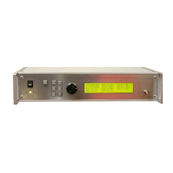
Page 19: Front Panel Controls (Units Without -Fpd Option)
FRONT PANEL CONTROLS (UNITS WITHOUT -FPD OPTION) 1. POWER Switch . This is the main power switch. When turning the instrument on, there is normally a delay of 10 seconds before anything is shown on the main display, as the internal operating system boots up. If the main menu does not appear after 30 seconds, turn off the instrument and leave it off for at least 60 seconds before applying power again. - Page 20 lists the key adjustable parameters and their current values. The “Programming Manual for -B Instruments” describes the menus and submenus in detail. 5. KEYPAD . Control Name Function MOVE This moves the arrow pointer on the display. CHANGE This is used to enter the submenu, or to select the operating mode, pointed to by the arrow pointer.
-
Page 21: Rear Panel Controls (Units Without -Fpd Option)
REAR PANEL CONTROLS (UNITS WITHOUT -FPD OPTION) GATE HV PULSE USED RS-232 DIFF TRIG PROBE GPIB Note: some connectors may be in different positions than shown above, depending on the exact combination of options ordered. 1. AC POWER INPUT . An IEC-320 C14 three-pronged recessed male socket is provided on the back panel for AC power connection to the instrument. - Page 22 length of cable attached to this input, and the source driving it, it may be desirable to add a coaxial 50 Ohm terminator to this input to provide a proper transmission line termination. The Pasternack (www.pasternack.com) PE6008-50 BNC feed-thru 50 Ohm terminator is suggested for this purpose.) 6.
- Page 23 arrangement. DO NOT CONNECT COAXIAL CABLING TO THIS OUTPUT. The capacitance of the cabling will reduce the dV/dt rates noticeably. 11. DIFF OUT Connector . This two-pin header connector connects internally to the logic output of the DUT (and the associated ground). This is the output that is monitored for “glitches”...
-
Page 24: Front Panel Controls (Units With -Fpd Option)
FRONT PANEL CONTROLS (UNITS WITH -FPD OPTION) 1. POWER Switch . This is the main power switch. When turning the instrument on, there is normally a delay of 10 seconds before anything is shown on the main display, as the internal operating system boots up. If the main menu does not appear after 30 seconds, turn off the instrument and leave it off for at least 60 seconds before applying power again. - Page 25 This overload indicator may flash yellow briefly at start-up. This is not a cause for concern. 3. SYNC OUT . This connector supplies a SYNC output that can be used to trigger other equipment, particularly oscilloscopes. This signal leads (or lags) the main output by a duration set by the "DELAY"...
- Page 26 be observed on an oscilloscope to accurately measure the dV/dt rate of the high voltage pulse. A Tektronix P5100 high-voltage probe with the 013-0291-00 probe-tip-to-BNC adapter, or a similar arrangement, should be used to connect to this output. CAUTION: Voltages as high as 1.5 kV may be present on the center conductor of this output connector.
-
Page 27: Rear Panel Controls (Units With -Fpd Option)
REAR PANEL CONTROLS (UNITS WITH -FPD OPTION) GATE TRIG RS-232 GPIB Note: some connectors may be in different positions than shown above, depending on the exact combination of options ordered. 1. AC POWER INPUT . An IEC-320 C14 three-pronged recessed male socket is provided on the back panel for AC power connection to the instrument. - Page 28 edge of this input. The input impedance of this input is 1 kΩ. (Depending on the length of cable attached to this input, and the source driving it, it may be desirable to add a coaxial 50 Ohm terminator to this input to provide a proper transmission line termination.
-
Page 29: General Information
GENERAL INFORMATION BASIC PULSE CONTROL This instrument can be triggered by its own internal clock or by an external TTL trigger signal. In either case, two output channels respond to the trigger: HV PULSE and SYNC. The HV PULSE channel is the signal that is applied to the DUT. Its amplitude is fixed, but the polarity is switchable. -
Page 30: Trigger Modes
The next figure illustrates the relationship between the signals when an external TTL- level trigger is used: > 50 ns TRIG TTL LEVELS (external input) (0V and 3V-5V) PROPAGATION DELAY (FIXED) 100 ns, FIXED SYNC OUT 3V, FIXED PULSE FALL TIME DELAY >... -
Page 31: Gating Modes
These modes can be selected using the front panel trigger menu, or by using the appropriate programming commands. (See the “Programming Manual for -B Instruments” for more details.) GATING MODES Triggering can be suppressed by a TTL-level signal on the rear-panel GATE connector. The instrument can be set to stop triggering when this input high or low, using the front- panel gate menu or the appropriate programming commands. -
Page 32: Dut Installation
A daughterboard arrangement is used to accommodate difference device packages and bias conditions. A zero-insertion force (ZIF) socket accepts these daughterboards. The AVRQ-5-B mainframe provides the high-voltage common mode pulse (which is tied to GND1), and VCC2 / GND2 (the non-floating output-side power supply). The user is responsible for configuring the daughterboards to implement the correct input side power (VCC1), biasing, filtering, loading, socketing, and glitch measurement. -
Page 33: Daughterboard Pinout
The socket and the sample daughterboards are designed so that the daughterboard can be installed in two positions – one for positive pulse mode, and one for negative pulse mode. This is explained further in the next section. DAUGHTERBOARD PINOUT The sample daughterboards have the pinout shown below:... - Page 34 For positive pulse mode, the “AMP1” front-panel setting must be set to a positive value AND the daughterboard must be installed in the socket so that it is in the left-most position (when viewed from the DUT area door opening), closest to the socket lever, like this: Unused space in this area...
- Page 35 most position (when viewed from the DUT area door opening), farthest from the socket lever, like this: 4 unused ZIF socket positions These silkscreened arrows must Daughterboard is always point in the same direction. installed as far to the right as possible, farthest from the lever.
-
Page 36: Daughterboard Components
ALWAYS ENSURE THAT THE SILKSCREENED ARROW ON THE DAUGHTERBOARD IS POINTING IN THE SAME DIRECTION AS THE ARROW ON THE MAINFRAME, AS SHOWN IN THE PHOTOS ABOVE. The instrument will not be damaged by inserting the daughterboard in the wrong position, as long as the arrows are aligned. - Page 37 0 - 300 pF). Do not exceed 600 pF, or the switching transistors may become overstressed and fail. The design files for the sample daughterboard (Avtech PCB 267C) are available for download at https://www.avtechpulse.com/semiconductor/avrq-5/#support_files. The function of the various components is summarized below:...
-
Page 38: Custom Daughterboards
CUSTOM DAUGHTERBOARDS The daughterboards provided with the AVRQ-5-B are meant as samples. The user may construct their own daughterboards, which may incorporated a preferred physical layout, different bias circuits, or different DUT packages and socketing. When designing your own daughterboard, take care to isolate the input and output sides as much as possible, to both provide sufficient high-voltage clearance and to minimize parasitic coupling of the HV pulse onto the output signal. -
Page 39: Installing The Daughterboards
If a non-differential probe is used, it is best to avoid measuring the low-voltage “DIFF OUT” signal at the same time as a probe is connected to the “HV PULSE” signal. Inter- channel interference in the probes and oscilloscope may introduce significant noise on the low-voltage signal. -
Page 40: Basic Test Arrangements
BASIC TEST ARRANGEMENTS The figure below shows the basic test arrangement for the AVRQ-5-B, with one possible DUT daughterboard configuration, with the daughterboard installed for positive pulse operation and a high-current input bias on the LED: In the above drawing, an HCPL-2601 current-drive opto-coupler is installed on the daughterboard, and the daughterboard is configured to drive the opto-coupler input with ~ 16 mA of current (using VCC1 and a 220 Ohm resistance). - Page 41 The figure below shows another basic test arrangement, with the daughterboard installed for negative pulse operation and zero input bias on the LED: In the above drawing, an HCPL-2601 current-drive opto-coupler is installed on the daughterboard, and the daughterboard is configured to drive the opto-coupler input with zero current (by jumpering pins 2 and 3 to GND1).
-
Page 42: Inter-Channel Interference
To connect the AVRQ-5-B properly, do the following: 1) With the power off, install an appropriately-configured daughterboard and DUT, as described in the previous sections. 2) Connect the SYNC output (on the front panel) to the external trigger input of the oscilloscope using (user-supplied) coaxial cabling. -
Page 43: Typical Waveforms For Standard Daughterboards
ZIF lever for the negative mode). The AVRQ-5-B front panel settings also control the DC voltage applied to VCC2 (+3 to +43V, adjustable, 150 mA maximum). This is the opto-coupler output-side bias. GND2 is connected to chassis ground. -
Page 44: Controlling The Transition Time
IMMUNITY (CMTI) CONTROLLING THE TRANSITION TIME The positive and negative pulse generators in the AVRQ-5-B are basically switched current sources. The voltage rise time can be controlled by deliberately soldering capacitance between the two “CAP” pads on the daughterboards (between the GND1 and GND2 signals). -
Page 45: Typical Positive Results, With No Dut Installed
TYPICAL POSITIVE RESULTS, WITH NO DUT INSTALLED The photos below show typical “HV PULSE” waveforms with with AMP1 = +1.5 kV, and a daughterboard installed in the ZIF socket in the positive position (silkscreen arrows pointing same direction, daughterboard is as close as possible to the ZIF lever), but with no DUT installed in the DIP8 socket on the daughterboard: C = 0 pF, t = 4.482 ns... -
Page 46: Typical Negative Results, With No Dut Installed
TYPICAL NEGATIVE RESULTS, WITH NO DUT INSTALLED The photos below show typical “HV PULSE” waveforms with with AMP1 = -1.5 kV, and a daughterboard installed in the ZIF socket in the negative position (silkscreen arrows pointing same direction, daughterboard is as far as possible from the ZIF lever), but with no DUT installed in the DIP8 socket on the daughterboard: C = 0 pF, t = 7.537 ns... -
Page 47: Vo3120 Results
VO3120 RESULTS A Vishay VO3120 was tested using VCC2 = +32V, and the following daughterboard configuration: Reference Value Typical Function Not used Load capacitance Not used Zero-Ohm Jumper to connect DUT pin 1 to VCC1 Not used Output pullup 348 Ω for 10 mA tests, Resistance to connect DUT pin 2 to VCC1. - Page 48 The actual daughterboard and DUT are shown below, configured for 10 mA of input bias current (with R3 = 348 Ohms and the A23 battery installed): Top side Bottom side With the daughterboard installed in the ZIF socket in the negative position (silkscreen arrows pointing same direction, daughterboard is as far as possible from the ZIF lever), and AMP1 set to -1.5 kV and AMP2 set to +32V, these waveforms were obtained:...
- Page 49 No significant logic output glitch for t No significant logic output glitch for t R10-90 R10-90 = 7.513 ns, so the CMTI exceeds 1.5 kV = 4.588 ns, so the CMTI exceeds 1.5 kV × (90%-10%) / 7.513 ns = 160 kV/us ×...
-
Page 50: Hcpl-7721 Results
HCPL-7721 RESULTS The HP / Agilent / Avago HCPL-7721 is a slower, older device. It was tested using VCC2 = +5V, and the following daughterboard configuration (including a rise time degradation capacitance): Reference Value Typical Function Not used Load capacitance 0 Ω... - Page 51 With the daughterboard installed in the ZIF socket in the negative position (silkscreen arrows pointing same direction, daughterboard is as far as possible from the ZIF lever), and AMP1 set to -1.5 kV and AMP2 set to +5V, these waveforms were obtained: Top = Logic output for 0V input Top = Logic output for 5V input Bottom = high voltage pulse...
- Page 52 Bottom side...
-
Page 53: Typical Waveforms For Customized Daughterboards
TYPICAL WAVEFORMS FOR CUSTOMIZED DAUGHTERBOARDS The following daughterboards are customized / special-order items. PCB 298B (FOR TLP2366) - Page 54 PCB 298B is similar to the standard sample daughterboard, except that it provides a footprint for a Toshiba TLP2366 in a 5-lead “SO6” SMT package. The DUT must be soldered to the daughterboard. (A DUT socket is not practical for these tests, since the extra parasitic capacitance introduced by a socket would severely degrade the measured CMTI.) Installation is similar to the standard daughterboards.
- Page 55 Top = Logic output for 0 mA input Top = Logic output for 6 mA input Bottom = high voltage pulse Bottom = high voltage pulse With the daughterboard installed in the ZIF socket in the negative position (silkscreen arrows pointing same direction, daughterboard is as far as possible from the ZIF lever), and AMP1 set to -1.5 kV and AMP2 set to +5V, these waveforms were obtained: Top = Logic output for 0 mA input Top = Logic output for 6 mA input...
- Page 56 Top side Bottom side A P6246 differential probe was used to observe the logic outputs in the TLP2366 tests.
-
Page 57: Pcb 299B (For Adum241E0Brwz)
PCB 299B (FOR ADUM241E0BRWZ) - Page 58 PCB 299B is similar to the standard sample daughterboard, except that it provides a footprint for an Analog Devices ADUM241E0BRWZ in a wide SO-16 SMT package. The DUT must be soldered to the daughterboard. (A DUT socket is not practical for these tests, since the extra parasitic capacitance introduced by a socket would severely degrade the measured CMTI.) Installation is similar to the standard daughterboards.
- Page 59 Top = Logic output for 0V input Top = Logic output for +5V input Bottom = high voltage pulse Bottom = high voltage pulse With the daughterboard installed in the ZIF socket in the negative position (silkscreen arrows pointing same direction, daughterboard is as far as possible from the ZIF lever), and AMP1 set to -1.5 kV and AMP2 set to +5V, these waveforms were obtained: Top = Logic output for 0V input Top = Logic output for +5V input...
- Page 60 Top side Bottom side A P6139A non-differential probe was used to observe the logic outputs in the TLP2366 tests, because the observed transients substantially exceeded the +/- 7V range of the P6246 differential probe.
-
Page 61: Capacitive Interference Issues
CAPACITIVE INTERFERENCE ISSUES The AVRQ-5-B requires the user to observe a logic-level output signal (typically 5V in amplitude) in the presence of a 1500 V pulse. This creates ample potential for interference, which can make it difficult to separate real glitches from measurement artifacts. - Page 62 A very large spurious signal is observed on the logic output! If the impedance of the logic output is reduced by adding a 1 kilohm pull-up resistor (R2 on the sample daughterboards) to VCC2 = +5V, a smaller transient of shorter duration is observed: Top: +1.5 kV HV pulse Top: -1.5 kV HV pulse Bottom: Logic out into open circuit...
- Page 63 The 1 kilohm impedance still results in a large voltage spike. If the pullup resistance is dramatically reduced to 50 Ohms, the coupled voltage spike is also reduced: Top: +1.5 kV HV pulse Top: -1.5 kV HV pulse Bottom: Logic out into open circuit Bottom: Logic out into open circuit no DUT, R2 = 1kΩ, 100 ns/div no DUT, R2 = 1kΩ, 100 ns/div...
- Page 64 Top: +1.5 kV HV pulse Top: -1.5 kV HV pulse Bottom: Logic out into open circuit Bottom: Logic out into open circuit HCPL-2601, R2 = 1kΩ, R6/9/10 = 0, HCPL-2601, R2 = 1kΩ, R6/9/10 = 0, 100 ns/div 100 ns/div Unfortunately, this makes it difficult to determine which transients are due to glitches transmitted inside the DUT and which are due to external capacitive coupling.
- Page 65 Some decaying LC-type oscillations are observed, due to the parasitic inductance in the circuit interacting with the parasitic capacitance. Similar results are obtained for the VO3120 when its input side is biased high rather than low: Top: +1.5 kV HV pulse Top: -1.5 kV HV pulse Bottom: Logic out into open circuit Bottom: Logic out into open circuit...
-
Page 66: Inductive Spikes And Probe Saturation
DUT. Some experimentation may be required by the user in order to identify the best probing arrangement. Early versions of the AVRQ-5-B were provided with sample daughterboards P/N 267B or earlier. (The current version is 267C). The earlier daughterboards used one pin to connect GND2 to the main board ZIF socket. - Page 67 If you are experiencing “unexpected” transients, keep in mind this possibility of probe saturation. (Users of AVRQ-5-B models with serial numbers below 13560 may wish to contact Avtech to have the additional pins of the ZIF socket wired for GND2 use, to reduce this effect.)
-
Page 68: Dc Correctness Issues
DC CORRECTNESS ISSUES The sample daughterboards provided with the AVRQ-5-B are designed to bias the input side of the optocoupler with a fixed bias during the test. To change it, components must be physically changed. This can be problematic with certain devices that do not necessarily power-up to a well-defined state. -
Page 69: Verification And Troubleshooting
VERIFICATION AND TROUBLESHOOTING It is sometimes unclear whether the glitches observed on the opto-coupler output are due to the opto-coupler or the test circuit. To reduce the number of sources of possible interference or error, a daughterboard scheme is used. This allows the drive conditions and the loading to be defined by simple, compact circuits that are user-visible and user-changeable. - Page 70 anything. If there is no change, that would tend to eliminate the drive signal as a source of problems. Some devices are simply very sensitive to ANY stray capacitance between the input and output sides. Some devices are extremely sensitive to interference coupled to pin 7, which (unwisely) provides a connection to the photo-transistor base.
-
Page 71: Safety Concerns
SAFETY CONCERNS TURN OUTPUT OFF BEFORE ACCESSING DUT Always turn the output off before opening the rear-panel DUT door, using the front panel menu or by computer command (“output off”). If you do not disable the output first, the output will be automatically disabled by a sensor on the DUT door when it is opened. -
Page 72: Operational Check
2. Turn on the AVRQ-5-B. The main menu will appear on the LCD. 3. To set the AVRQ-5-B to trigger from the internal clock at a PRF of 10 Hz: a) The arrow pointer should be pointing at the frequency menu item. If it is not, press the MOVE button until it is. - Page 73 d) Press CHANGE to return to the main menu. 5. To set the HV PULSE amplitude to +1.5 kV: a) Press the MOVE button until the arrow pointer is pointing at the AMP1 menu item. b) Press the CHANGE button. The submenu will appear. Rotate the ADJUST knob until the amplitude is set at +1.5 kV.
-
Page 74: Protecting Your Instrument
PROTECTING YOUR INSTRUMENT USE HIGH-VOLTAGE CABLES, CONNECTORS, AND PROBES Confirm that the scope probe and any adapters used on the HV PULSE output are rated for at least 1.5 kV (2 kV for -XHV units) pulsed operation. SHORT-CIRCUIT PROTECTION The output will withstand temporary short-circuit conditions. However, short-circuit conditions should not be allowed to persist longer than 10 seconds, or the stress on the components will shorten the circuit lifetime. -
Page 75: Mechanical Information
There are no user-adjustable internal circuits. For repairs other than fuse replacement, please contact Avtech (info@avtechpulse.com) to arrange for the instrument to be returned to the factory for repair. Caution: High voltages (over 2000V) are present inside the instrument during normal operation. -
Page 76: Maintenance
MAINTENANCE REGULAR MAINTENANCE This instrument does not require any regular maintenance. Traceable calibration of the pulse parameters should be established using a calibrated measurement of the output, rather than relying on instrument settings. On occasion, one or more of the four rear-panel fuses may require replacement. All fuses can be accessed from the rear panel. -
Page 77: Programming Your Pulse Generator
PROGRAMMING YOUR PULSE GENERATOR KEY PROGRAMMING COMMANDS The “Programming Manual for -B Instruments” describes in detail how to connect the pulse generator to your computer, and the programming commands themselves. A large number of commands are available; however, normally you will only need a few of these. -
Page 78: All Programming Commands
ALL PROGRAMMING COMMANDS For more advanced programmers, a complete list of the available commands is given below. These commands are described in detail in the “Programming Manual for -B Instruments”. (Note: this manual also includes some commands that are not implemented in this instrument. - Page 79 *OPC *SAV 0 | 1 | 2 | 3 [no query form] *RCL 0 | 1 | 2 | 3 [no query form] *RST [no query form] *SRE <numeric value> *STB? [query only] *TST? [query only] *WAI [no query form]...
-
Page 80: Wiring Diagrams
WIRING DIAGRAMS WIRING OF AC POWER Mains circuits - hazardous live. Do no t attem pt a ny rep airs on this i nstr ume nt beyon d the fuse repla cement p ro cedures de scrib ed i n the manual. C ontact A v tech if the i nstr ument A3 - B LA CK r equi res serv icing. -
Page 81: Wiring Of +54Vdc Power Rail
2) INS TALL C31 = 2.2uF CER 3) INS TALL C29 = C30 = 47uF/35V 4) INS TALL L6, L8 = 7447452101 (100uH) 5) INS TALL J12 = 640456-4 +54V PS FOR AVRQ-5-B, AVRQ-4-B-SCHB Pri nte d Re vis i on 19-Sep-2017... -
Page 82: Pcb 158R2 - Low Voltage Power Supply
PCB 158R2 - LOW VOLTAGE POWER SUPPLY... -
Page 83: Pcb 104F - Keypad / Display Board, 1/3
PCB 104F - KEYPAD / DISPLAY BOARD, 1/3 Amp 5 4 9 9 9 1 0 -1 , 1 0 p in strai g h t h ead er LC D-BU TT LC D-BU TT. SCH SD A SD A SC L SC L GN D... -
Page 84: Pcb 104F - Keypad / Display Board, 2/3
PCB 104F - KEYPAD / DISPLAY BOARD, 2/3 U4 A VC C C1 0 VC C BU T1 VC C 2 . 2 u F C1 5 C1 3 0 . 1 u F 0 . 1 u F 0 . 1 u F 0 . -
Page 85: Pcb 104F - Keypad / Display Board, 3/3
PCB 104F - KEYPAD / DISPLAY BOARD, 3/3 VC C VC C 0 . 1 u F 2 . 2 u F GN D VC C VC C VC C SD A SD A SC L SC L GN D PA D3 PA D4 PC F8 5 7 4 AN (MU ST HA VE "A"... -
Page 86: Dut Wiring, On Main Pcb
DUT WIRING, ON MAIN PCB FOR US ER 'S LOGIC P ROBE LOGIC OU TPU T SA M1 0 3 7 -0 1 -ND FR OM P OW E R SU PP LY CI RC UITS VC C2 GN D2 VC C2 -PS 4 3 4 -0 1 -4 71 J 0 . -
Page 87: Dut Wiring, On Standard Daughterboard (Pcb 267C)
DUT WIRING, ON STANDARD DAUGHTERBOARD (PCB 267C) -
Page 88: Dut Wiring, On Customized Tlp2366 Daughterboard (Pcb 298B)
DUT WIRING, ON CUSTOMIZED TLP2366 DAUGHTERBOARD (PCB 298B) -
Page 89: Dut Wiring, On Customized Adum241E0Brwz Daughterboard (Pcb 299B)
DUT WIRING, ON CUSTOMIZED ADUM241E0BRWZ DAUGHTERBOARD (PCB 299B) -
Page 90: Main Wiring
IXFH 5 8 N 20 . ISOL ATE W ITH SIL-P AD . OU T BD 3 PC B 29 5 B +2 4 V, N O OLO AVRQ-5-B. -AHV, -XHV, -FPD, -V2 OPTIONS. Pri nte d Re vis i on 19-Sep-2017 Z:\mjcfiles\circuits\avr-N\avr-N.Ddb - AVRQ-5-B\AVRQ-5 V4.s ch... -
Page 91: Performance Check Sheet
PERFORMANCE CHECK SHEET...
Need help?
Do you have a question about the AVRQ-5-B and is the answer not in the manual?
Questions and answers