JVC TH-V70 Service Manual
Dvd digital theater system
Hide thumbs
Also See for TH-V70:
- Instructions manual (91 pages) ,
- Instructions manual (86 pages) ,
- Instructions manual (84 pages)
Advertisement
Quick Links
SERVICE MANUAL
DVD DIGITAL THEATER SYSTEM
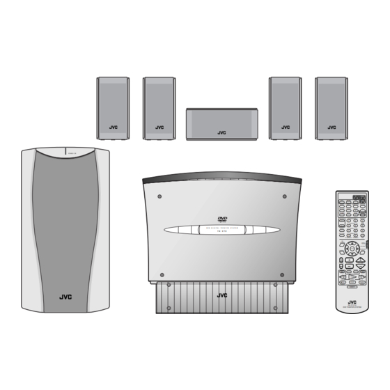
SP-XSV70
SP-PWV70
Contents
Safety precautions
Preventing static electricity
Importance administering point
on the safety
SP-XSV70
SP-XCV70
XV-THV70
1-2
1-3
1-4
COPYRIGHT
2002 VICTOR COMPANY OF JAPAN, LTD.
J ----------------------------- U.S.A.
C -------------------------- Canada
SP-XSV70
SP-XSV70
Area suffix
1-6
1-21
1-22~54
No.21089
Jul. 2002
Advertisement

Related Manuals for JVC TH-V70


Summary of Contents for JVC TH-V70
-
Page 1: Table Of Contents
TH-V70 SERVICE MANUAL DVD DIGITAL THEATER SYSTEM TH-V70 Area suffix J ----------------------------- U.S.A. C -------------------------- Canada SP-XSV70 SP-XSV70 SP-XCV70 SP-XSV70 SP-XSV70 SP-PWV70 XV-THV70 Contents Safety precautions Disassembly method Preventing static electricity Adjustment method 1-21 Importance administering point Description of major ICs... -
Page 2: Th-V70
TH-V70 1. This design of this product contains special hardware and many circuits and components specially for safety purposes. For continued protection, no changes should be made to the original design unless authorized in writing by the manufacturer. Replacement parts must be identical to those used in the original circuits. Services should be performed by qualified personnel only. - Page 3 TH-V70 Preventing static electricity 1. Grounding to prevent damage by static electricity Electrostatic discharge (ESD), which occurs when static electricity stored in the body, fabric, etc. is discharged, can destroy the laser diode in the traverse unit (optical pickup). Take care to prevent this when performing repairs.
- Page 4 TH-V70 Importance administering point on the safety <Main body section> Main board F901 Caution: For continued protection against risk of fire, replace only with same type 1.6A/125V for F901. This symbol specifies type of fast operating fuse. Precaution: Pour eviter risques de feux, remplacez le fusible de surete de F901 comme le meme type que 1.6A/125V.
- Page 5 TH-V70 <Speaker section> Power supply & SP terminal board F403 Mother board F505 F504 Caution: For continued protection against risk of fire, replace only with same type 4A/125V for F403, 8A/125V for F504, 8A/125V for F505. This symbol specifies type of fast operating fuse.
-
Page 6: Disassembly Method
TH-V70 Disassembly method Top plate <Main body section> Removing the top plate (See Fig. 1.) From the top side of the main body, remove the four screws A attaching the top plate. Fig.1 Top panel Removing the bottom panel (See Figs. 2 and 3.) From the rear side of the main body, remove the three screws B attaching the bottom panel. - Page 7 TH-V70 Removing the DVD mechanism DVD mechanism assembly (See Figs. 5 and 6.) assembly Remove the top plate. Remove the bottom panel. Remove the top panel. LED board From the top side of the main body, disengage the CN812 claw c of the DVD mechanism assembly and then remove the push button.
- Page 8 TH-V70 Removing the DSP/Audio board (See Figs. 9 and 10.) Remove the top plate. Remove the bottom panel. Compulink board Tuner Remove the top panel. Remove the DVD mechanism assembly. DSP/Audio CN592 board From the top side of the main body, remove a screw G attaching the DSP/Audio board.
- Page 9 TH-V70 Removing the main board (See Figs. 11 and 12.) Insert this wire into the notch. Remove the top plate. Compulink board Main board Remove the bottom panel. Tuner Remove the top panel. Remove the DVD mechanism assembly. Card wire Remove the front panel assembly.
- Page 10 TH-V70 <Front panel assembly section> Door motor assembly Remove the top plate. Switch board Remove the bottom panel. Remove the top panel. Remove the DVD mechanism assembly. Remove the front panel assembly. Removing the switch board (See Fig. 15.) Front panel assembly...
- Page 11 TH-V70 <DVD mechanism assembly section> Claw a Remove the top plate. Remove the bottom panel. LED board Remove the top panel. Remove the DVD mechanism assembly. Removing the LED board (See Fig. 1.) From the top side of the DVD mechanism...
- Page 12 TH-V70 Removing the DVD traverse mechanism assembly (See Fig. 4.) DVD traverse mechanism assembly Remove the DVD servo board. Remove the two screws C attaching the DVD traverse mechanism assembly. Disengage the claw f attaching the DVD traverse mechanism assembly and then take out the DVD traverse mechanism assembly.
- Page 13 TH-V70 Attaching the DVD pickup unit Section j (See Figs. 5 to 9.) DVD pickup unit [Reference] Refer to the explanation of "Removing the DVD pickup unit" on the preceding page. Attach the SW. actuator and shaft to the DVD pickup unit.
- Page 14 TH-V70 Removing the feed motor (See Figs. 12 to 14.) Remove the DVD servo board. Remove the DVD traverse mechanism assembly. Remove the four screws G attaching the traverse Traverse mechanism assembly. mechanism Mechanism assembly base Take out the traverse mechanism assembly from the mechanism base.
- Page 15 TH-V70 Removing the switch board (See Fig.15.) CD mechanism assembly Clamper base assembly Remove the DVD mechanism assembly. From the top side of the CD mechanism assembly, remove the screw J attaching the switch board. Lift the switch board slightly and then remove the wire from connector CN101 on the switch board.
- Page 16 TH-V70 <Speaker section> Amplifier assembly Removing the amplifier assembly (See Figs. 1 and 2.) From the rear side of the speaker main body, remove the four screws A attaching the heat sink cover and then remove the heat sink cover.
- Page 17 TH-V70 Removing the pre-amplifier board (See Figs. 4 to 6.) Mother board Remove the rear panel. Remove the two screws F attaching the volume bracket. Heat sink Disconnect the pre-amplifier board from the Volume bracket connector CN201 on the mother board and take out the pre-amplifier board.
- Page 18 TH-V70 Removing the mother board Mother board (See Figs. 7 and 8.) Remove the rear panel. Power amplifier Remove the pre-amplifier board. board (A) Remove the power supply & SP terminal board. Disconnect the wire from the connector CN104 on the mother board.
- Page 19 TH-V70 Removing the power amplifier board (B) (See Figs. 9 and 11.) Remove the mother board. Remove the four screws N attaching the heat sink CN106 to the power amplifier board (B). (See Fig.9.) P.TR holder (B) (Bottom side) From the bottom side of the power amplifier board Power amplifier (B), disengage the four engagement sections c.
- Page 20 TH-V70 Removing the LED indicator (See Figs. 14 to 16.) Insert the tip of a flat-bladed screwdriver or a similar tool into the space between the speaker main body and the ornament panel (the section Ornament panel indicated by the arrows), and lift the net little by little to remove.
-
Page 21: Adjustment Method
TH-V70 Adjustment method Initializing in TEST MODE Initializing in TEST MODE Press the power button on the main unit, and put Moving panel close? it in standby. Make sure that the panel has closed. While pressing both the STOP button (fourth button from left) Pull out the power plug. -
Page 22: Description Of Major Ics 1-22~54
TH-V70 Description of major ICs AN8703FH (IC101) : Frontend processor for DVD 1.Terminal layout LPC1 RFINN LPCO1 RFINP LPC2 TESTSG LPCO2 AGCO VFOSHORT AGCG TBAL PEAK FBAL BOTTOM AN8703FH POFLT RFENV DTRD IDGT OFTR STANDBY DCRF VCC3 STDIO RFOUT RSCL... - Page 23 TH-V70 Pin No. Symbol Function DFLTOP Filter amplifier positive output DCFLT Filter output capacitance connection GND3 Ground 3 RFDIFO Radial differential output (Not use) RFOUT RF full-addition amplifier output VCC3 Power supply 3 (3.3V) Filter for RF-group delay correction amplifier...
- Page 24 TH-V70 MN101C49GKD1 (IC801) : System micon 1.Terminal layout 2. Pin function Pin No. Symbol Function VREF- Connect to ground NTSEL(RGB--SEL) NTSC/PAL discrimination(RGB/YC switching discrimination) signal VER/HOR SEL Vertical/Horizontal setting discrimination signal Slide door switch1 PHOTOSW Loading mechanism photo switch LOCK...
- Page 25 TH-V70 Pin No. Symbol Function DSP-STAT DSP serial communication data input DSP-CLK DSP serial communication clock VOL-DATA VOLUME serial communication data output VOL-STB VOLUME serial communication strobe VOL-CLK VOLUME serial communication clock Slide door switch2 INT/PROG D terminal LINE2 switching...
- Page 26 TH-V70 MN102L62GLF1 (IC401) : Unit CPU 1. Terminal layout 2. Pin function Pin No. Symbol Function WAIT Micro computer wait signal input Read enable /SPMUTE Spindle muting output to IC251 Write enable Not connect Chip select for ODC Chip select for ZIVA (Not connect)
- Page 27 TH-V70 Pin No. Symbol Function Not connect Communication request Connect to TP405 (REQ) Not connect Ground EPCS EEPROM chip select EPSK EEPROM clock EPDI EEPROM data input EPDO EEPROM data output Power supply SCLKO Communication clock S2UTD Communication input data...
- Page 28 TH-V70 MN103S26EGA (IC301) : Optical disc controller 1.Terminal layout 2. Pin function Pin No. Symbol Function NINT0 System control interruption 0 NINT1 System control interruption 1 VDD3 Power supply (3.3V) Ground NINT2 System control interruption 2 WAITODC System control wait control...
- Page 29 TH-V70 Pin No. Symbol Function TILT Not connect TILTN Not connect Not connect DTRD Not connect IDGT Not connect VDD18 Power supply (1.8V) Ground VDD3 Power supply (1.8V) OSCI1 16.9MHz clock input OSCO1 Not connect Ground TSTSG Calibration signal VFOSHORT...
- Page 30 TH-V70 Pin No. Symbol Function RF envelope input DVD laser current control terminal Tracking drive IC input offset CD laser current control terminal TECAPA Not connect VDD3 Power supply (3.3V) Ground 127 - 130 MONI0 - 3 Internal goods title monitor (Connect to TP306 - TP309)
- Page 31 TH-V70 TC9446F-025 (IC403) : DSP 1.Terminal layout 2. Pin function Pin No. Symbol Function Reset signal input terminal (L: reset, H: normal operation) MIMD Mode select input for MCU interface (L: serial, H: IIC bus) MICS Chip select input for MCU interface...
- Page 32 TH-V70 Pin No. Symbol Function PLON Clock selection input (L: external clock, H: VCO clock) AMPI Amplifier input for low pass filter AMPO Amplifier output for low pass filter External clock input VSSA Analog ground DIR clock output LOCK VCO lock output...
- Page 33 TH-V70 Pin No. Symbol Function LPFO Low pass filter output for DLL circuit DLON DLCKS pin DLON pin DLL clock setting DLCKS "L" "L" SCKI input (DLL = off) "L" "H" 4th times of XI clock "H" "L" 3rd times of XI clock "H"...
- Page 34 TH-V70 NDV8601VWA-BB (IC501) : DVD on a chip processor 1.Terminal layout 2. Pin function Pin No. Symbol Function Vddio Power supply (3.3V) MD10,MD11 SDRAM data bus Power supply (1.8V) MD12 SDRAM data bus Vssio Ground 7 - 9 MD13 - MD15...
- Page 35 TH-V70 Pin No. Symbol Function 54 - 56 MD23 - MD25 SDRAM data bus Vssio Ground 58 - 61 MD26 - MD29 SDRAM data bus Vddio Power supply (3.3V) 63,64 MD30,MD31 SDRAM data bus DQM3 SDRAM data byte enable CS1-...
- Page 36 TH-V70 Pin No. Symbol Function OSCVss Oscillator ground OSCVdd Oscillator power supply (1.8V) MVCKVdd Main and video clock PLL power supply (3.3V) SCEN Scan chain test enable MVCKVss Main and video clock PLL ground ACLKVss Audio clock PLL ground SCMD...
- Page 37 TH-V70 Pin No. Symbol Function Vssio Ground 163 - 168 AD13 - AD8 P multiplexed address/data bus Vddio Power supply (3.3V) PWE1- Byte write enable for FLASH, EEPROM,SRAM or peripherals Ground 172 - 176 AD7 - AD3 P multiplexed address/data bus...
- Page 38 TH-V70 UPD784215AGC167 (IC406) : DSP micom 1. Terminal layout 2. Pin function Pin No. Symbol Function 1 - 8 Not connect Power supply OSC connect pin OSC connect pin Ground Not connect Not connect RESET Reset input AUTODATA Data request signal...
- Page 39 TH-V70 Pin No. Symbol Function CODEC_D-OUT CO decoder digital data output CODEC_D-IN CO decoder digital data input (Not connect) CODEC_CLK CO decoder clock signal CODEC_CS CO decoder chip select signal CODEC_XTS Not connect 69,70 Not connect Power down and Reset in...
- Page 40 TH-V70 MN101C35DKB (IC701) : FL driver microcomputer 1. Terminal layout 2. Pin function Pin No. Symbol Function Not connect DATAIN FL driver communication data input/output CLOCK FL driver communication clock input Not connect INITIAL FL driver communication CS(INITIAL) Not connect...
- Page 41 TH-V70 AK93C65AF (IC510) : EEPROM 1. Terminal layout 2. Pin function Pin No. Symbol Function Not connect, Program enable (With built-in pull-up resistor) Power supply Chip selection Cereal clock input Cereal data input Cereal data output Ground Not connect 8 PIN SOP NOTE : The pull-up resistor of the PE pin is about 2.5M...
- Page 42 TH-V70 AK4527BVQP (IC401) : A/D,D/A Converter 1.Terminal layout 2.Block diagram Audio LIN+ LIN- DZF2 SDOS RIN+ RIN+ RIN- RIN- SMUTE LIN+ BICK LRCK LIN- LRCK LOUT1 DATT BICK ROUT1 SDTI1 D.AUX MCLK LOUT1 SDTI2 ROUT1 DATT ROUT2 SDTI3 Format LOUT2...
- Page 43 TH-V70 Pin No. Symbol Function X'tal oscillator Select/Test mode pin "H" : X'tal Oscillator selected "L" : External clock source selected Input clock select 1 pin (Not connect) ADIF Input clock select 0 pin CAD1 Chip address pin Used during the serial control mode.
- Page 44 TH-V70 BA15218F (IC510,IC511,IC531,IC561,IC581,IC591) : Dual operational amplifier 1. Terminal layout & Block diagram OUT1 IN1- OUT2 IN1+ IN2- IN2+ BA15218N (IC103,IC104,IC108,IC109,IC110,IC201,IC202) : Dual operational amplifier 1. Terminal layout & Block diagram BA15218N OUT1 -IN1 +IN1 +IN2 -IN2 OUT2 BA3121 (IC100,IC101,IC102) : Ground isolation amplifier 1.
- Page 45 TH-V70 BA5983FM (IC201) : 4-channel driver 1. Terminal layout & Block diagram 2. Pin function Pin No. Symbol Function BIASIN Input for Bias-amplifier OPIN1+ Non inverting input for CH1 OP-AMP OPIN1- Inverting input for CH1 OP-AMP OPOUT1 Output for CH1 OP-AMP...
- Page 46 TH-V70 BA6664FM (IC251) : Motor driver 1. Terminal layout & Block diagram GAIN SHORT BRAKE SWITCH TORQE BRAKE MODE SENSE AMP. HALL BIAS CURRENT SENSE AMP. GAIN DRIVER CONTROL HALL AMP. 2. Pin function Pin No. Symbol Function Not connect...
- Page 47 TH-V70 CY24203SC (IC502) : Clock generator 1. Terminal layout 2. Block diagram XOUT OUTPUT DIVIDERS 16.9344M XOUT 7 bit 7 bit VCXO 13.5M 11bit VCXO 16.9344M 8 bit 13.5M GP1FA351RZ (IC409) : Fiber optic receiver 1. Terminal layout 2. Block diagram Vout Comp &...
- Page 48 TH-V70 K4S643232E-TC60 (IC505) : 512K x 32 bit x 4 banks synchronous DRAM 1. Terminal layout 2. Block diagram Data Input Register Bank Select LDQM 512K x 32 512K x 32 512K x 32 512K x 32 Column Decoder Latency & Burst Length...
- Page 49 TH-V70 LA73054 (IC601) : Video driver 1. Terminal layout & block diagram DRIVER DRIVER DRIVER DRIVER DRIVER DRIVER LPF2 LPF1 2Step Amp1 LPF2 LPF1 LPF2 LPF1 2Step Amp4 LPF1 SYNC C_OFFSET LPF1 2Step 2Step DC_CTL 2Step Amp5 Amp6 PEDESTAL Amp3...
- Page 50 TH-V70 M62446FP (IC153) : 6CH Master volume 1. Terminal layout & Block Diagram DVDD OUTPUT volume DATA PORT DGND AVDD volume LFE IN AGND AGND LFE OUT volume RR IN RR OUT RL IN RL OUT AGND C OUT volume...
- Page 51 TH-V70 Pin No. Symbol Function L/R volume input terminal AVSS Analog negative power supply terminal L ch output L OUT R OUT R ch output C OUT Center volume signal output terminal RL OUT L ch volume signal output terminal for rear speaker...
- Page 52 TH-V70 NJM4580M (IC158,IC159,IC160) : Dual operational amplifier 1. Terminal layout & Block diagram B OUT B -IN B +IN A OUT A -IN A +IN NJM78M05FA (IC805,IC953) : Regulator 1. Terminal layout 2. Block diagram INPUT 1.INPUT 2.GND OUTPUT 3.OUTPUT PQ05RD21 (IC951) : Regulator 1.
- Page 53 TH-V70 SST39VF160-7CEK (IC509) : 16 Mbit multi-purpose flash memory 1. Terminal layout */BYTE */RST Top view *R/B 2. Block diagram Super flash memory X-Decoder Memory Address Address buffer & Latches Y-Decoder I/O Buffers and Data Latches Control Logic D15 - D0 3.
- Page 54 TH-V70 STK402-030 (IC106) : Power amplifier 1.Terminal layout 2.Block diagram ch. 1 ch. 2 STK402-030 +Vcc BIAS +VCC -VCC -Vcc STK402-230 (IC107) : Power amplifier 1. Terminal layout STK402-230 2.Block diagram ch. 1 ch. 2 ch. 3 -Vcc +Vcc BIAS...
- Page 55 TH-V70 < M E M O > 1-55...
-
Page 56: Th-V70
TH-V70 VICTOR COMPANY OF JAPAN, LIMITED AUDIO & COMMUNICATION BUSINESS DIVISION PERSONAL & MOBILE NETWORK BUSINESS UNIT. 10-1,1Chome,Ohwatari-machi,maebashi-city,371-8543,Japan No.21089 200207...
Need help?
Do you have a question about the TH-V70 and is the answer not in the manual?
Questions and answers