Table of Contents
Advertisement
Quick Links
SERVICE MANUAL
XV-S500BK / XV-S502SL
TV
DVD
STANDBY/ON
OPEN/
CLOSE
TV
DVD
TV1
TV2
TV3
1
2
3
TV4
TV5
TV6
4
5
6
TV7
TV8
TV9
7
8
9
TV-/--
TV0
MUTING
10
0
+10
TITLE/
TV/VIDEO
RETURN
SUBTITLE
GROUP
CANCEL
CH
+
VOL-
VOL+
ENTER
CH
-
PREVIOUS
NEXT
CLEAR
SELECT
STROBE
SLOW-
SLOW+
REPEAT
SUBTITLE
AUDIO
VFP
PROGRESSSIVE
STANDBY/ON
SCAN
DIGEST
ANGLE
ZOOM
3D
PHONIC
AMP VOL
RM-SXV008J
REMOTE CONTROL
Contents
Safety precautions ------------------------- 1-2
Preventing static electricity -------------- 1-3
Importance admistering
point on the safety --------- 1-4
Precautions for service ------------------- 1-5
Disassembly method ---------------------- 1-6
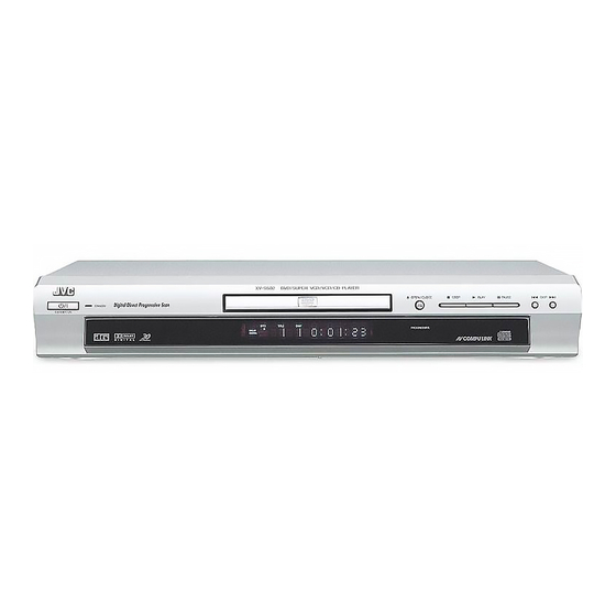
DVD VIDEO PLAYER
DVD/SUPER VCD/VCD/CD PLAYER
STANDBY
Each difference point
Model
XV-S500BK
XV-S502SL
This service manual is printed on 100% recycled paper.
COPYRIGHT
2002 VICTOR COMPANY OF JAPAN, LTD.
XV-S500BK / XV-S502SL
0
7
3
8
OPEN/CLOSE
STOP
PLAY
PAUSE
PROGRESSIVE
Body color
Black
Silver
Adjustment method ------------------------ 1-15
Confirm method of operation ------------- 1-20
Troubleshooting ---------------------------- 1-21
Description of major ICs ------------------ 1-25
Glossary of term and abbreviations ---- 1-46
Area Suffix
J ------------- U.S.A.
C ---------- Canada
4
SKIP
No.A0027
Feb. 2002
Advertisement
Table of Contents

Related Manuals for JVC XV-S500BK


Summary of Contents for JVC XV-S500BK
-
Page 1: Table Of Contents
XV-S500BK / XV-S502SL SERVICE MANUAL DVD VIDEO PLAYER XV-S500BK / XV-S502SL Area Suffix J ------------- U.S.A. C ---------- Canada STANDBY/ON OPEN/ CLOSE TV-/-- MUTING TITLE/ TV/VIDEO RETURN SUBTITLE GROUP CANCEL VOL- VOL+ ENTER PREVIOUS NEXT CLEAR SELECT STROBE DVD/SUPER VCD/VCD/CD PLAYER... - Page 2 XV-S500BK/XV-S502SL 1. This design of this product contains special hardware and many circuits and components specially for safety purposes. For continued protection, no changes should be made to the original design unless authorized in writing by the manufacturer. Replacement parts must be identical to those used in the original circuits. Services should be performed by qualified personnel only.
-
Page 3: Preventing Static Electricity
XV-S500BK/XV-S502SL Preventing static electricity Electrostatic discharge (ESD), which occurs when static electricity stored in the body, fabric, etc. is discharged, can destroy the laser diode in the traverse unit (optical pickup). Take care to prevent this when performing repairs. 1.1. Grounding to prevent damage by static electricity Static electricity in the work area can destroy the optical pickup (laser diode) in devices such as DVD players. -
Page 4: Point On The Safety
XV-S500BK/XV-S502SL Importance Admistering point on the Safety P901 J703 S802 J700 B118 S801 J802 J702 C1800 C707 J701 J804 J801 C747 R777 B229 C757 C813 Q753 Q743 R765 R775 R766 B102 C1701 C815 C808 L1701 T1701 C746 R1721 C756 B875... -
Page 5: Precautions For Service
XV-S500BK/XV-S502SL Precautions for Service Handling of Traverse Unit and Laser Pickup 1. Do not touch any peripheral element of the pickup or the actuator. 2. The traverse unit and the pickup are precision devices and therefore must not be subjected to strong shock. -
Page 6: Disassembly Method
XV-S500BK/XV-S502SL Disassembly method <Main body> Removing the top cover (see Fig.1) 1.Remove the two screws A attaching the top cover on both sides of the body. 2.Remove the three screws B attaching the top A x 2 cover on the back of the body. - Page 7 XV-S500BK/XV-S502SL Removing the rear panel (see Fig.5) *Prior to performing the following procedure, remove Rear panel the top cover. 1.Remove the nine screws D attaching the rear panel on the back of the body. Fig.5 Removing the front panel assembly Hook d (see Fig.6,7)
- Page 8 XV-S500BK/XV-S502SL <Loading assembly section> Removing the clamper assembly Joint a Joint a (See Fig.1) Remove the four screws A attaching the clamper assembly. Move the clamper in the direction of the arrow to release the two joints a on both sides.
- Page 9 XV-S500BK/XV-S502SL Removing the traverse mechanism assembly (See Fig.4 and 5) Prior to performing the following procedure, remove the clamper assembly and the tray. Traverse mechanism Remove the four screws B attaching the traverse assembly mechanism assembly. ATTENTION: Before reattaching the traverse...
- Page 10 XV-S500BK/XV-S502SL Removing the motor assembly (See Fig.8 and 9) Belt Prior to performing the following procedure, remove the clamper assembly, the tray, the traverse mechanism assembly and the elevator. Remove the belt from the pulley. Remove the screw C attaching the motor assembly.
- Page 11 XV-S500BK/XV-S502SL Pulley gear Idle gear Pulley gear bracket Pulley gear Idle gear Pulley gear bracket Tads h Pulley gear Motor assembly Fig.10 Slide cam Removing the Idle gear / pulley gear / middle gear / slide cam (See Fig.10 to 12)
- Page 12 XV-S500BK/XV-S502SL <Traverse mechanism assembly section> Feed motor assembly Removing the feed motor assembly (See Fig.13) Unsolder the two soldering j on the spindle motor board. Remove the two screws F attaching the feed motor assembly. Pickup Notch k Soldering j...
- Page 13 XV-S500BK/XV-S502SL Removing the pickup (See Fig.16 and 17) Pickup Joint n Remove the screw I attaching the T spring (S) and Shaft holder the shaft holder. Remove also the plate. ATTENTION: When reattaching, make sure that the T spring (S) presses the shaft.
- Page 14 XV-S500BK/XV-S502SL Spindle motor Removing the spindle motor assembly (See Fig.19 to 21) Remove the three screws L attaching the spindle motor on the bottom of the mechanism base. ATTENTION: When reattaching, pass the card wire extending from the spindle motor board through the notch of the spindle base.
-
Page 15: Adjustment Method
XV-S500BK/XV-S502SL Adjustment method (1) Test mode setting method 1) Take out the disc and close the tray. 2) Unplug the power plug. 3) Insert power plug into outlet while pressing both "PLAY" key and "STOP" key of the main body. - Page 16 XV-S500BK/XV-S502SL (4) Display of current value of laser 1) Makes to test mode and initializes. 2) When "CHOICE" key of remote controller is pushed three times, It is displayed on the FL display, "CHECK". 3) Afterwards, the laser current value can be switched by pushing the key to remote controller without turning on the disc.
- Page 17 XV-S500BK/XV-S502SL (6) Upgrading of firmware 1) The power supply is turned on pushing the "POWER" key. 2) The up-grade disc is inserted. 3) When FL display of the main body changes from "READING" into "UPGRADE", cursor "UP" key ( ) of remote controller is pushed.
- Page 18 XV-S500BK/XV-S502SL Flap adjustment of the pick-up guide shaft Assistance board <Tool list for adjustment> (Connect to main board) Stud (four pieces set) Parts No. : JIGXVS40 XV-S40 MAIN CONNECT Extension cord set (two cord and two board) Parts No. : EXTXVS40CB...
-
Page 19: Attention When Pick-Up Is Exchanged
XV-S500BK/XV-S502SL Attention when pick-up is exchanged Switch actuator 1.Flexible wire, pick-up spring, switch actuator, and lead spring are removed from an old pick-up Lead spring (broken the one). < Guide > Pick-up Flexible wire, pick-up spring and switch actuator, lead spring are removed without each decomposing while assembled. -
Page 20: Confirm Method Of Operation
The EEPROM is initialized. Refer to the initialization method. Opening picture check (Power ON) It should be display "JVC" Muting working The noise must not be had to the performance beginning when you push "PLAY" button or at ON/STANDBY. -
Page 21: Troubleshooting
XV-S500BK/XV-S502SL Troubleshooting Servo volume Press OPEN /CLOSE key Is tray Confirmation of tray drive circuit operation and circuit in surrounding correct? Is the traverse moving See "(3) Traverse movement error" along the innermost in "Check points for individual errors" perimeter for SW detection? "NO DISC"... - Page 22 XV-S500BK/XV-S502SL Check points for each error (1) Spindle start error 1.Defective spindle motor *Are there several ohms resistance between each pin of CN201 "5-6","6-7","5-7"? (The power supply is turned off and measured.) *Is the sign wave of about 100mVp-p in the voltage had from each terminal? [ CN201"9"(H1-),"10"(H1+),"11"(H2-),"12"(H2+),"13"(H3-),"14"(H3+) ]...
- Page 23 XV-S500BK/XV-S502SL (3) Traverse movement NG 1.Defective traverse driver *Has the voltage come between terminal of CN101 "1" and "2" ? 2.Defective BTL driver (IC201) *Has the motor drive voltage gone out to IC201"17" or "18"? 3.Has the control signal come from servo IC or the microcomputer? *Is it "H"...
- Page 24 XV-S500BK/XV-S502SL (9) Neither picture nor sound is output 1.It is not possible to search *Has the tracking been turned on? *To "(5) Tracking ON NG" in "Check points for each error" when the tracking is not normal. *Is the feed operation normal? To "(3) traverse movement NG"...
-
Page 25: Description Of Major Ics
XV-S500BK/XV-S502SL Description of major ICs 74LCX373MTC-X(IC512,IC513) 1.Pin layout 2.Pin function 3.Truth table INPUTS OUTPUTS Symbol Description D0~D7 Data inputs Latch enable input Output enable input Q0~Q7 3-State latch outputs H = HIGH Voltage level L = LOW Voltage level Z = High impedance... - Page 26 XV-S500BK/XV-S502SL AN8703FH-V (IC101) : Frontend processor 1.Pin layout 2.Pin function Symbol Description Symbol Description Pin No. Pin No. Laser input terminal (DVD) RFDIFO LPC1 Non connect LPC01 Laser drive signal output terminal (DVD) RFOUT Connect to TP103 LPC2 Laser input terminal (CD) VCC3 Power supply terminal 3.3V...
- Page 27 XV-S500BK/XV-S502SL BA6664FM-X (IC251) : 3Phase Motor Driver 1.Pin layout 2.Block diagram DRIVER GAIN SWITCH GAIN CONTROL CURRENT SENSE AMP HALL AMP TOROUE SENSE AMP SHORT BRAKE CK Q BRAKE MODE Hall Bias 1-27...
- Page 28 XV-S500BK/XV-S502SL 3.Pin function BA6664FM-X Symbol Description Pin No. Non connect Output 3 for spindle motor Non connect Output 2 for spindle motor Non connect Non connect Output 1 for spindle motor Connect to ground Positive input for hall input AMP 1...
- Page 29 XV-S500BK/XV-S502SL K4S643232E-TC60(IC505):DRAM 1.Block diagram Data input register LDQM Bank select 512K x 32 512K x 32 512K x 32 512K x 32 Column decoder Latency & burst length LCKE Programming register LRAS LCBR LDQM LCAS LWCBR Timing register 2.Pin function...
- Page 30 XV-S500BK/XV-S502SL MM1568AJ-X (IC801) : Video driver 1.Pin layout and block diagram Vcc1 Vcc2 BIAS 150kohm 75ohm COUT Driver 6.75MHz MUTE1 GND2 sync tip clamp 75ohm VOUT Driver 6.75MHz YC MIX VSAG sync tip clamp GND2 6.75MHz 75ohm BIAS YOUT BIAS...
- Page 31 XV-S500BK/XV-S502SL MN101C35DLE (IC2) : System controller 1.Pin layout 2.Pin function (1/2) Symbol Description Pin No. Unused RS232COUT Unused RS232CIN Unused Power supply terminal (+5V) Clock output terminal OSC2 Clock input terminal OSC1 Connect to ground Connect to ground Non connect...
- Page 32 XV-S500BK/XV-S502SL 2.Pin function (MN101C35DLE 2/2) Symbol Description Pin No. Standby LED control signal output (RED) Standby LED control signal output (GREEN) Progressive LED control signal output (RED) Progressive LED control signal output (GREEN) Unused FL Grid control signal output 52~64...
- Page 33 XV-S500BK/XV-S502SL MN102L62GLF1 (IC401) : Unit CPU Pin function Symbol Function Symbol Function Pin No. Pin No. Micon wait signal input Non connect WAIT SWUPDN Read enable Connect to ground MECHA_H/V Spindle muting output to IC251 Mechanism state signal input SPMUTE...
- Page 34 XV-S500BK/XV-S502SL MN103S26EGA (IC301) : Super optical disc controller 1.Terminal layout 2.Block diagram Host I/F DVD-ROM Analog MPEG I/F Formatter CD-PRE ATAPI High speed IO bus Instruction Servo I/O CGEN memory (core 1 I/O) (40KB) 32 bit CPU core 2Mbit Servo core...
- Page 35 XV-S500BK/XV-S502SL 3.Pin function (MN103S26EGA : 2/4) Symbol Description Pin No. Read signal input from system controller System control data 37~44 CPUDT7~0 Non connect CLKOUT1 Test mode switch signal MMOD System reset NRST Master terminal polarity switch input MSTPOL Non connect...
- Page 36 XV-S500BK/XV-S502SL 3.Pin function (MN103S26EGA : 3/4) Symbol Description Pin No. PLFLT1 Connect to capacitor 1 for PLL AVSS Connect to ground for analog circuit Connect to resistor for VREF reference current source VREFH Reference voltage input (2.2V) PLPG Non connect VHALF Reference voltage input (1.65V)
- Page 37 XV-S500BK/XV-S502SL 3.Pin function (MN103S26EGA : 4/4) Symbol Description Pin No. Connect to ground VDD3 Power supply terminal for I/O (3.3V) HDD1 ATAPI host data 1 HDD13 ATAPI host data 13 HDD2 ATAPI host data 2 HDD12 ATAPI host data 12...
- Page 38 XV-S500BK/XV-S502SL MN35505-X (IC703) : DAC 1.Terminal layout LRCK DVDD1 DVDD2 VCOF DVSS2 XOUT DVSS1 OUT1C OUT2C AVDD1 AVDD2 OUT1D OUT2D AVSS1 AVSS2 2. Pin function Pin No. Symbol Description Control signal for DAC Digital data input LRCK L and R clock for DAC...
- Page 39 XV-S500BK/XV-S502SL NDV8601VWA-BB(IC501):AV Decoder 1.Pin layout 2.Block diagram digital audio Video I/O port audio DAC NTSC Audio MPEG Video Audio digital audio output Video output Video SCART processor decoder processor encoder Serial serial XBUS port XBUS peripherals controller controller DVD,A/V RISC...
- Page 40 XV-S500BK/XV-S502SL 3.Pin function (NDV8601VWA-BB 2/4) Symbol Description Pin No. Non connect MA11 Connect to ground VSSio 32,33 SDRAM Address bus, reserved for terminal compatibility with 64Mb SDRAM MA12,13 Power supply terminal 1.8V SDRAM Primary bank chip select Power supply terminal 3.3V...
- Page 41 XV-S500BK/XV-S502SL 3.Pin function (NDV8601VWA-BB 3/4) Symbol Description Pin No. Power supply terminal 3.3V VDDio SSP0 Data out or UART0 data-terminal-ready signal SSPOUT0 UART0 Serial data output to an external serial device TXD0 UART0 Serial data input from external serial device...
- Page 42 XV-S500BK/XV-S502SL 3.Pin function (NDV8601VWA-BB 4/4) Symbol Description Pin No. External bus clock used for programmable host peripherals SCLK Programmable WAIT/ACK/RDY control Connect to ground VSSio 163~168 Multiplexed address / data bus terminal AD13~8 Power supply terminal 3.3V VDDio Byte write enable for FLASH,EEPROM,SRAM or peripherals terminal...
- Page 43 XV-S500BK/XV-S502SL S-93C66AFJ-X (IC451,IC510) : EEPROM 1.Pin layout 2.Pin function Pin No. Symbol Description Non connect Power supply terminal Chip select input Serial clock input Serial data input Serial data output Connect to ground Non connect 3.Block diagram Memory Address array...
- Page 44 XV-S500BK/XV-S502SL SST39VF160-7CEK (IC509) : 16M EEPROM 1. Pin layout /BYTE /RST 2. Block diagram 16,777,216Bit EEPROM X-Decoder Cell Array A19~A0 Address Buffer & Latches Y-Decoder Control Logic I/O Buffers & Data Latches DQ15~DQ0 3. Pin function Symbol Pin name Function...
- Page 45 XV-S500BK/XV-S502SL STR-G6651-F8 (IC901) : Switch regulator 1.Block diagram 2.Pin function Pin No. Symbol Description Function Drain terminal MOS FET drain Source terminal MOS FET source Ground terminal Ground Power supply terminal Input of power supply for control circuit O.C.P/F.B Over current / Feedback terminal...
-
Page 46: Glossary Of Term And Abbreviations
XV-S500BK/XV-S502SL Glossary of term and abbreviations (for AV Decoder section) 3-dimension 1)audio/video 2)audio/visual alternating current ACLK audio serial-data (bit) clock multiplexed address / data bus analog-to-digital converter digital audio input address latch enable ANSI/SMPTE American National Standards Institute / Society of Motion Pictures and Television Engineers... - Page 47 XV-S500BK/XV-S502SL MCLK primary or master clock Megahertz MIPS Million Instructions Per Second MmCPU Mediamatics CPU (synonym for internal RISC CPU) Moving Picture Experts Group Layer-3 Audio (audio file format / extension) MPEG1 audio A digital audio format mainly used in video CDs. It is based on the moving picture expert group (MPEG1) format, a data compression technology.
- Page 48 XV-S500BK / XV-S502SL VICTOR COMPANY OF JAPAN, LIMITED PERSONAL & MOBILE NETWORK BUSINESS UNIT 1644, Shimotsuruma, Yamato, Kanagawa 242-8514, Japan Printed in Japan No.A0027 200202(S)
Need help?
Do you have a question about the XV-S500BK and is the answer not in the manual?
Questions and answers