Advertisement
Quick Links
Download this manual
See also:
Instruction Manual
SERVICE MANUAL
DVD AUDIO/VIDEO PLAYER
Contents
Safety precautions ------------------------ 1-2
Preventing static electricity ------------- 1-3
the traverse unit ----- 1-4
Important for laser products ------------ 1-5
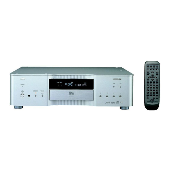
XV-D9000
Disassembly method -------------------- 1-7
Description of major ICs ---------------- 1-19
This service manual is printed on 100% recycled paper.
COPYRIGHT
2001 VICTOR COMPANY OF JAPAN, LTD.
J ------------- U.S.A.
on the safety ----- 1-6
and display of jitter value ----- 1-18
XV-D9000
Area Suffix
No.A0004
Mar. 2001
Advertisement

Subscribe to Our Youtube Channel
Related Manuals for JVC XV-D9000


Summary of Contents for JVC XV-D9000
-
Page 1: Table Of Contents
XV-D9000 SERVICE MANUAL DVD AUDIO/VIDEO PLAYER XV-D9000 Area Suffix J ------------- U.S.A. Contents Safety precautions ------------------------ 1-2 Importance admistering point Preventing static electricity ------------- 1-3 on the safety ----- 1-6 Dismantling and assembling Disassembly method -------------------- 1-7 the traverse unit ----- 1-4... - Page 2 XV-D9000 1. This design of this product contains special hardware and many circuits and components specially for safety purposes. For continued protection, no changes should be made to the original design unless authorized in writing by the manufacturer. Replacement parts must be identical to those used in the original circuits.
-
Page 3: Preventing Static Electricity
XV-D9000 Preventing static electricity Electrostatic discharge (ESD), which occurs when static electricity stored in the body, fabric, etc. is discharged, can destroy the laser diode in the traverse unit (optical pickup). Take care to prevent this when performing repairs. 1.1. Grounding to prevent damage by static electricity Static electricity in the work area can destroy the optical pickup (laser diode) in devices such as DVD players. -
Page 4: Dismantling And Assembling
XV-D9000 Dismantling and assembling the traverse unit 1. Notice regarding replacement of optical pickup Electrostatic discharge (ESD), which occurs when static electricity stored in the body, fabric, etc. is discharged, can destroy the laser diode in the traverse unit (optical pickup). Take care to prevent this when performing repairs to the optical pickup or connected devices. -
Page 5: Important For Laser Products
XV-D9000 Important for Laser Products 5.CAUTION : If safety switches malfunction, the laser is able 1.CLASS 1 LASER PRODUCT to function. 2.DANGER : Invisible laser radiation when open and inter 6.CAUTION : Use of controls, adjustments or performance of lock failed or defeated. Avoid direct exposure to beam. -
Page 6: Importance Admistering Point
XV-D9000 Importance Admistering point on the Safety Full Fuse Replacement Marking Marquage Pour Le Remplacement Complet De Fusible Graphic symbol mark Le symbole graphique (Ce symbole signifie (This symbol means fast blow type fuse.) fusible de type a fusion rapide.) should be read as follows ;... -
Page 7: Disassembly Method
XV-D9000 Disassembly method Top panel <Main body> Removing the top panel(See Fig.1) 1.Remove the eight screws A by hexagonal driver attaching the top panel. 2.A top panel is lifted up and it is removed. Removing the side panel(See Fig.1) Fig.1 1.Remove the four screws B by hexagonal driver... - Page 8 XV-D9000 Rear cover Removing the rear cover(See Fig.6~8) *Prior to performing the following procedure, remove the top panel. 1.Remove the eighteen screws E attaching the rear cover from back of the main body. 2.Remove the three screws F attaching the Fig.6...
- Page 9 XV-D9000 Removing the DVD mechanism assembly DVD Mechanism assembly cover (See Fig.9~11) *Prior to performing the following procedure, remove the top panel and main board. 1.Remove the four screws I attaching the DVD mechanism assembly cover, and DVD mechanism assembly cover lifted up and it is removed.
- Page 10 XV-D9000 Removing the audio(rear L/R) board (See Fig.12~13) *Prior to performing the following procedure, remove the top panel and rear cover. 1.Remove the three screws L attaching the audio(rear L/R) board. 2.Remove the four screws M attaching the audio(rear L/R) board from back of the body.
- Page 11 XV-D9000 Removing the video signal board(See Fig.15,16) CN503 CN502 *Prior to performing the following procedure, remove the top panel and rear cover. 1.Remove the three screws P attaching the video signal board. 2.Remove the five screws Q attaching the video signal board from back of the body.
- Page 12 XV-D9000 Removing the signal processing board (See Fig.19) Signal processing board *Prior to performing the following procedure, remove the top panel. CN711 1.Remove the four screws V attaching the signal processing board. CN741 2.Disconnect the connector from CN711 and CN741 on the signal processing board.
- Page 13 XV-D9000 Removing the operation switch board/ FL and operation switch board(See Fig.22) 1.Remove the front panel assembly.(See Fig.1~5) 2.Remove the ten screws Y attaching the FL and operation switch board. 3.Remove the seven screws Z attaching the operation switch board.
- Page 14 XV-D9000 Loading tray <Removing DVD mechanism unit> Removing the clamper base (See Fig.1) * Remove the top cover. * Remove the DVD mechanism unit. 1. Remove the two screws A attaching the clamper base. Clamper base Removing the loading tray (See Fig.2~4) * Remove the clamper base.
- Page 15 XV-D9000 Traverse mechanism unit Removing the traverse mechanism unit (See Fig.5) * Remove the loading tray. 1. Remove the three screws B attaching the traverse mechanism unit. Protecting the optical pickup * Solder the flexible ground point on the optical pickup when replacing the pickup or before detaching the mechanism control board.
- Page 16 XV-D9000 Traverse chassis Removing the turntable and spindle motor assembly (See Fig.8~9) * Remove the traverse mechanism unit. * Solder the flexible ground point on the optical pickup. (See Fig.6) * Remove the mechanism control board. 1. Remove the flexible harness from the feed motor connector on the spindle motor board assembly.
- Page 17 XV-D9000 Loading base Lever Removing the loading mechanism parts (See Fig.10~11) * Remove the clamper base. Up-down * Remove the disk tray. Pawl a 1. Turn the lever counterclockwise until it stops (position 1), while pushing the switch lever in the direction of the arrow and pushing up the pawl at a using a screwdriver.
-
Page 18: Method Of Initializing Eeprom
XV-D9000 Method of initializing EEPROM and display of jitter value Initializing EEPROM Please initialize EEPROM when you exchange Microcomputer(IC401,IC402) and optical pick-up by the undermentioned method. 1. It is confirmed that there is no disk in the tray. 2. The power supply plug is inserted while pushing the PLAY key and the OPEN/CLOSE key to the main body. -
Page 19: Description Of Major Ics
XV-D9000 Description of major ICs ADV7123KST50(IC359):Video DAC BLANK BLANK AND SYNK SYNK LOGIC DATA R9-R0 REGISTER DATA G9-G0 REGISTER DATA B9-B0 REGISTER POWER-DOWN VOLTAGE PSAVE VREF REFERENCE MODE CIRCUIT CLOCK RSET COMP Pin Function (1/2) Function Symbol Pin No. 1~10... - Page 20 XV-D9000 AN8706FHQ (IC101) : Front end processor 1.Pin layout RDCKP CBDOFS RDCKN RBCA RDTP TESTSG RDTN RFINP GND5 RFINN GND4 VCC2 VCC4 GND2 DTMONN VREF2 DTMONP COFTFS DSLFLT COFTSL DSLO RFON FLTOUT RFOP DCFLT AN8706FHQ VREF3 DCRF VPWBDO VPWOFT VIN6...
- Page 21 XV-D9000 3.Pin function AN8706FHQ (1/2) Pin No. Symbol Functions LDONB Laser ON (CD Head) terminal LDONA Laser ON (DVD Head) terminal LPCOA Laser drive output terminal LPC1 Laser PIN input terminal VHARF VHALF voltage output terminal TGBAL Tangential phase balance control terminal...
- Page 22 XV-D9000 3.Pin function AN8706FHQ(2/2) Pin No. Symbol Functions Power terminal 5 (3.3V) VCC5 IDGT Data slice part address part gate signal input terminal (For RAM) DTRD Data slice data read signal input terminal(For RAM) CAPA Data slice CAPA(Address)signal input terminal (For RAM)
- Page 23 XV-D9000 BA5983FM-X (IC271) : 4CH DRIVER 1.Block diagram STAND BY Level Shift Level Shift Level Shift Level Shift STAND BY CH1/2/3 2.Pin function Function Symbol Symbol Function Pin No. Pin No. Input for Bias-amplifier VO4(+) Non inverted output of CH4...
- Page 24 XV-D9000 IS61LV256-12T(IC163,IC164,IC165,IC173):32k X 8 Low voltage CMOS Static RAM 1.Pin layout 2.Block diagram I/O7 256 X 1024 A0-A14 DECODER I/O6 MEMORY ARRAY I/O5 I/O4 I/O3 I/O2 I/O1 I/O0 I/O0-I/O7 COLUMN I/O DATA CIRCUIT 3.Pin function CONTROL Function Pin No. Symbol...
- Page 25 XV-D9000 JCE8011(IC551):Graphic controller Pin No. Symbol Function VD0~7 DVD Image signal input (Multi plex data Y,Cr,Cb) VCLKI Dot clock signal input (27MHz) HSYNCI The horizontal synchronous signal input VSYNCI Vertical synchronous signal input Power supply VCLKO Dot clock signal output (27MHz)
- Page 26 XV-D9000 JCV8005-2(IC471):CPPM 1.Pin layout 2.Pin function JCV8005-2 1/2 Description Pin No. Symbol Power supply Connect to ground Data input/output terminal (both by 8 bits) 3~10 HDATA0~7 Power supply Connect to ground 8 bit address bus to internal address (connect to host)
- Page 27 XV-D9000 2.Pin function JCV8005-2 2/2 Symbol Description Pin No. Connect to ground Glue logic output signal to host WAIT1 Non connect WAIT2 Glue logic input signal (connect to 27 pin) WAITIN Power supply Connect to ground Connect to ground TEST_IN...
- Page 28 XV-D9000 M27C1602CZ(IC402,IC553):16M ROM 1.Pin layout BYTE 2.Pin function Symbol Symbol Pin No. Function Pin No. Function Write enable Power supply +3.3V Address bus 19 Data bus 4 Address bus 18 Data bus 12 Address bus 8 Data bus 5 Address bus 7...
- Page 29 XV-D9000 M30622EC-FP(IC451):System controller 1.Pin layout 100 ~ 81 31 ~ 50 2.Key Matrix KEY IN 0 KEY IN 1 KEY IN 2 KEY OUT 0 DISPLAY OFF POWER KEY OUT 1 PAUSE OPEN/CLOSE STOP KEY OUT 2 PLAY 3.Pin Function (1/2)
- Page 30 XV-D9000 3.Pin Function (2/2) M30622EC-FP Function Symbol Pin No. Latch output for K2 K2LATCH Switch output for PLL PLLSEL1 Switch output for PLL PLLSEL0 Sub woofer mute output LMUTE Center mute output CMUTE Surround mute output SMUTE Front mute output...
- Page 31 XV-D9000 M66004SP(IC802):FL DRIVER 1.Block diagram Vcc2 SEG35 Display code SEG27 CGROM register (35bit 160) (8bit 16) SEG26 SEG00 FLCS Serial reception FLCK circuit CGRAM FLDATA (35bit 16) RAM write Output port (2bit) Display control RESET code select register DIG11 Clock...
- Page 32 XV-D9000 MBM29LV2TC9TN(IC357):2Mbit Flash memory 1.Pin layout 2.Pin function (TOP VIEW) Symbol Pin function Address inputs A-1,A0~A16 BYTE Data inputs / outputs DQ0~DQ15 Chip enable Output enable Write enable Ready / busy output RY/BY Hardware reset pin / Temporary sector RESET N.C.
- Page 33 XV-D9000 MC44724AVFU (IC554) : VIDEO ENCODER 1.Terminal layout 2.Block diagrams 64 ~ Y/G1Vdd DVdd Copy, Sync_ generator CVBS/Cb/B1Vdd protection DVss C/Cr/R1Vdd CGMS, CCwss gen wss gen Y/G1 Y/G1 CVBS/Cb/B1 off_set DVIA[7:0] CVBS/Cb/B1 DEMAX C/Cr/R1 DVIB[7:0] C/Cr/R1 Modulator A/B_sel Vref1 iBIAS1...
- Page 34 XV-D9000 MN102LP25G(IC401):UNIT CPU Function Symbol Symbol Function Pin No. Pin No. Micon wait signal input Detection switch of tray close WAIT SWCLOSE Read enable Detection switch of tray open SWOPEN Driver mute Serial enable signal for ADSC MUTE ADSCEN Write enable...
- Page 35 XV-D9000 MN103007BGA (IC301) : Optical disc controller 1.Pin layout HDD15 SBCK HDD0 HDD14 5VDD HDD1 PVDD HDD13 PVSS HDD2 OSC01 HDD12 OSCI1 HDD3 LRCK HDD11 BLKCK HDD4 IPFLAG HDD10 DACCLK 5VDD DACLRCK HDD5 DACDATA HDD9 NTRON MN103007BGA HDD6 JMPINH HDD8...
- Page 36 XV-D9000 3.Pin function MN103007BGA(1/2) Symbol Function Symbol Function Pin NO. Pin NO. HDD15 ATAPI data CPUADR8 System control address CPUADR7 HDD0 ATAPI data System control address HDD14 ATAPI data CPUADR6 System control address CPUADR5 5VDD System control address HDD1 ATAPI data...
- Page 37 XV-D9000 3.Pin function MN103007BGA(2/2) Symbol I/O Function Symbol I/O Function Pin NO. Pin NO. ATAPI slave master diagnosis input Land / group switch NPDIAG NTRON Tracking ON ATAPI host address DACDATA Cereal output ATAPI output of selection of width DACLRCK...
- Page 38 XV-D9000 MN4SV17160BT-10(IC504,IC505,IC352,IC353):16MB SDRAM 1.Block diagram Column decoder Sense amplifier Bank 0 Memory cell array Column 2048 Row x 256 address Column x 16 bit counter Column address Column decoder buffer Sense amplifier DQ15 Bank 1 Memory cell array address buffer...
-
Page 39: Block Diagram
XV-D9000 MN67705EA(IC201):Digital servo controller 1.Pin layout AVSS LDONA TS(AD1) LDONB FS(AD2) PULIN FE(AD3) TROFS(AD4) DVSS TE(AD5) TRAYSET1 VREFLDA TRAYSET2 VREFMDA DRVMUTE VREFHDA DVDD TG(AD6) TRVSW N.C.(AD7) TRAY-CLOSE N.C.(AD8) TRAY-OPEN RFENV(AD9) ST/SP VREFOP MN67705 HFMON LDCUR(AD10) JITOUT(AD11) DVSS VREFC PLLOK AVDD(AD12) N.C. - Page 40 XV-D9000 3.Pin function MN67705EA (1/3) Pin No. Symbol Function H fixation LDONA Laser drive controlA (ON / OFF) LDONB Laser drive controlB (ON / OFF) PULIN DSL and PLL high boost signal (FEP) Head amplifier gain H/L selection DVSS Ground for digital circuit...
- Page 41 XV-D9000 3.Pin function MN67705EA (2/3) Pin No. Symbol Function IREF3 Connects with unused DVSS VCOF2 Connects with unused DVSS DVSS Ground for digital circuit VCOE3 Connects with unused DVSS DVSS Ground for digital cirucuit DVDD Power supply for digital cirucuit...
- Page 42 XV-D9000 3.Pin function MN67705EA(3/3) Pin No. Symbol Function FS (FEP) FS(AD2) TS (FEP) TS(AD1) Ground for analog circuit AVSS Power supply for analog circuit AVDD Focus balance(FEP) FBAL(DA1) Cutting off frequency (FEP) FC(DA2) Amount of boost (FEP) BOOST(DA3) DSL offset balance (FEP)
- Page 43 XV-D9000 MN8271AT(IC351):I/P Converter Pin Function (1/3) Function Symbol Pin No. VIN6~0 Video data signal input Connect to ground 9~11 IICAD0~2 IIC Slave address input IICSCL IIC Transfer clock input IICSDA IIC Data input/output Power supply terminal XRST Processor reset signal input (L:active)
- Page 44 XV-D9000 Pin Function (2/3) MN8271AT Function Symbol Pin No. PPLLPDN SVP-PE PLL,power down Power supply terminal Video data signal output 60~63 VOUT0~3 Connect to ground 65~68 VOUT4~7 Video data signal output Power supply terminal 70~73 VOUT8~11 Video data signal output...
- Page 45 XV-D9000 Pin Function (3/3) MN8271AT Function Symbol Pin No. SDCK SDRAM Clock signal output Power supply terminal SDRAM Clock enable SDCKE 153,154 SDA9,SDA8 SDRAM Address data output Power supply terminal 156~159 SDA7~4 SDRAM Address data output Connect to ground 161,162...
- Page 46 XV-D9000 MX27L1000TC-15(IC172,IC162):PROM 1.Pin layout 2. Block diagram Control Output Q0-Q7 Logic Buffer Y-Decoder Y-Select A0-A16 Address Input 1M Bit X-Decoder cell matrix 3.Pin function TC74AC393FT-X(IC715) : Dual binary counter 1.Pin layout 2.Truth table INPUTS OUTPUTS 1CLR 2CLR COUNT UP NO CHANGE...
- Page 47 XV-D9000 TC74ACT153F-X(IC183):Dual 4-channel multiplexer 1.Pin layout (TOP VIEW) 2.Truth table SELECT DATA INPUTS OUTPUT STORE INPUTS X:Don't Care TC74HC08AP(IC915) / TC74HCT08AP(IC916):2-input and gate TC74VHC08FT-X(IC722) / TC74VHCT08AFT-X(IC721):2-input and gate 1.Pin layout 2.Truth table (TOP VIEW) 1-47...
- Page 48 XV-D9000 TC74HC74AF-W(IC181):Dual D-type flip flop preset and clear TC74VHC74FT-X (IC726,IC725) 1.Pin layout 2.Truth table 1CLR INPUTS OUTPUTS FUNCTION 2CLR CLEAR PRESET (TOP VIEW) NO CHANGE X : Don't Care TC74VHC03F-X(IC182):2-input nand gate 1.Pin layout 2.Truth table L : High impedance...
- Page 49 XV-D9000 TC74VHCT32AF-X (IC723) : Buffer 1. Pin layout 2.Truth table 1A 1 14 Vcc 1B 2 13 4B 1Y 3 12 4A 2A 4 11 4Y 2B 5 10 3B 2Y 6 GND 7 TC74VHCT541AFTX (IC358) : Buffer 1. Pin layout, Block diagram 2.
- Page 50 XV-D9000 TC7WH74FU-X(IC713,IC716) : Clock buffer 1.Pin layout 2.Truth table INPUTS OUTPUTS FUNCTION CLEAR PRESET NO CHANGE X : Don't Care 1-50...
- Page 51 XV-D9000 XCF56362PV100(IC161,IC171):DSP Pin Function (1/2) Function Symbol Pin No. SCK/SCL SPI Serial clock / IC Serial clock SS/HA2 SPI Slave select signal input / IC Slave address 2 input HREQ Host request signal input/output SDO0 Serial data output 0 SDO1...
- Page 52 XV-D9000 Pin Function (2/2) XCF56362PV100 Function Symbol Pin No. GNDP1 PLL Ground 1 terminal VCCQH Quiet external (high) power supply terminal AA3/RAS3 Address attribute or Row address strobe AA2/RAS2 Address attribute or Row address strobe Column address strobe Debug event...
- Page 53 XV-D9000 ZIVA3-PE0(IC501) : AV Decoder ZIVA3-PEO (1/5) Function Symbol Pin No. Programmable I/O pins.Input mode after reset. PIO0 8-bit bi-directional host data bus. writes data to the decoder Code FIFO via HDATA. HDATA0 MSB of the 32-bit word is written first. The host also reads and writes the decoder HDATA1 internal registers and local SDRAM via HDATA.
- Page 54 XV-D9000 ZIVA3-PEO (2/5) Function Symbol Pin No. PIO28 PIO29 Programmable I/O pins. Output mode after reset PIO30 VDD-3.3 3.3-V supply voltage for I/O signals. PIO31 Programmable I/O pins. Output mode after reset Ground for core logic and I/O signals. No Connection Programmable I/O pins.
- Page 55 XV-D9000 ZIVA3-PEO (3/5) Function Symbol Pin No. MADDR8 Memory address. MADDR10 VDD-3.3 3.3-V supply voltage for I/O signals. MADDR7 Memory address. Ground for core logic and I/O signals. MADDR0 MADDR6 Memory address. MADDR1 VDD-3.3 3.3-V supply voltage for I/O signals.
- Page 56 XV-D9000 ZIVA3-PEO (4/5) Function Symbol Pin No. VDD-3.3 3.3-V supply voltage for I/O signals. VDATA4 Video data bus. Byte serial CbYCrY data synchronous with VCLK. At power-up, the decoder does not drive VDATA. During boot-up, the decoder uses configuration parameters to drive or 3-state VDATA Ground for core logic and I/O signals.
- Page 57 XV-D9000 ZIVA3-PEO (5/5) Function Symbol Pin No. DVD parallel compressed data from DVD DSP. When DVD DSP sends 32-bit words, it must write DVD-DATA7 the MSB first. /CDG-SCLK CDG-SDATA:CD+G (Sub code) Data.Indicates serial sub code data input. DVD-DATA6 CDG-VSFY:CD+G (Sub code)Frame Sync. Indicates frame-start or composite synchronization /CDG-SOS1 input.
- Page 58 XV-D9000 VICTOR COMPANY OF JAPAN, LIMITED PERSONAL & MOBILE NETWORK BUSINESS UNIT 1644, Shimotsuruma, Yamato, Kanagawa 242-8514, Japan Printed in Japan No.A0004 200103(S)
Need help?
Do you have a question about the XV-D9000 and is the answer not in the manual?
Questions and answers