Yamaha DCU5D Service Manual
Digital cabling unit
Hide thumbs
Also See for DCU5D:
- Owner's manual (8 pages) ,
- Brochure & specs (14 pages) ,
- Manual de instrucciones (13 pages)
Table of Contents
Advertisement
Quick Links
Download this manual
See also:
Owner's Manual
QQ
3 7 63 1515 0
TE
L 13942296513
.
PA
011861
200706- オープンプライス
DIGITAL CABLING UNIT
x
u163
y
i
2 9
8
SERVICE MANUAL
SERVICE MANUAL
Q Q
3
6 7
1 3
1 5
CONTENTS(目次)
SPECIFICATIONS(総合仕様) ..................................................3
DIMENSIONS(寸法図) .............................................................3
PANEL LAYOUT(パネルレイアウト) .......................................4
CIRCUIT BOARD LAYOUT(ユニットレイアウト) .....................5
DISASSEMBLY PROCEDURE (分解手順) ...............................6
LSI PIN DESCRIPTION(LSI 端子機能表) ..............................10
IC BLOCK DIAGRAM(IC ブロック図) ...................................15
CIRCUIT BOARDS(シート基板図) ........................................18
BLOCK DIAGRAM(ブロックダイアグラム)
co
.
Copyright (c) Yamaha Corporation. All rights reserved. PDF
9 4
2 8
0 5
8
2 9
9 4
2 8
m
HAMAMATSU, JAPAN
9 9
9 9
'07.09
Advertisement
Table of Contents

Related Manuals for Yamaha DCU5D


Summary of Contents for Yamaha DCU5D
-
Page 1: Table Of Contents
CIRCUIT BOARD LAYOUT(ユニットレイアウト) .....5 DISASSEMBLY PROCEDURE (分解手順) .......6 LSI PIN DESCRIPTION(LSI 端子機能表) ......10 IC BLOCK DIAGRAM(IC ブロック図) ........15 CIRCUIT BOARDS(シート基板図) ........18 PARTS LIST BLOCK DIAGRAM(ブロックダイアグラム) u163 CIRCUIT DIAGRAM(回路図) 011861 HAMAMATSU, JAPAN 200706- オープンプライス Copyright (c) Yamaha Corporation. All rights reserved. PDF ’07.09... -
Page 2: Http://Www.xiaoyu163.Com
IMPORTANT NOTICE This manual has been provided for the use of authorized Yamaha Retailers and their service personnel. It has been assumed that basic service procedures inherent to the industry, and more specifically Yamaha Products, are already known and understood by the users, and have therefore not been restated. -
Page 3: Specifications(総合仕様
DCU5D 3 7 63 1515 0 SPECIFICATIONS(総合仕様) • General Specifi cations Normal Rate: 42.9975–49.200 kHz Sampling Frequency Double Rate: 85.995–98.400 kHz Power Requirements 12 W Dimensions 480 x 150 x 44 mm (W x D x H) Net Weight 2.3 kg... -
Page 4: Panel Layout(パネルレイアウト
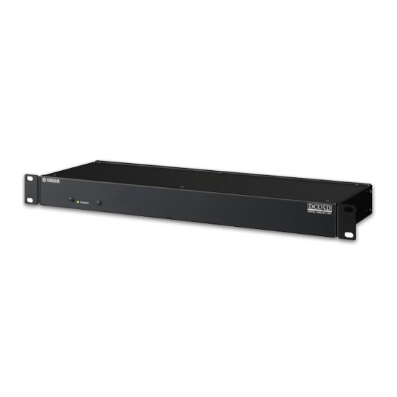
DCU5D 3 7 63 1515 0 PANEL LAYOUT(パネルレイアウト) • Front Panel(フロントパネル) POWER • Rear Panel(リアパネル) CASCADE IN TX RX TX RX POWER AC IN 1P:GND 4P:12V L 13942296513 q [POWER] Indicator q [POWER]インジケーター w Mode switch w モードスイッチ e Ground screw e アース用ネジ... -
Page 5: Circuit Board Layout(ユニットレイアウト
DCU5D 3 7 63 1515 0 CIRCUIT BOARD LAYOUT(ユニットレイアウト) Power supply unit (電源ユニット) AC inlet (ACインレット) ES-CS L 13942296513 u163... -
Page 6: Disassembly Procedure(分解手順
DCU5D 3 7 63 1515 0 DISASSEMBLY PROCEDURE(分解手順) Precautions ( 注意事項) Install the fi lament tape and the harness clamp in the ※ フィラメントテープ、束線止めは、取り外す前と同じよ うに取り付けてください。 same way as they were before removal. Notes on Flat Cable ※ フラットケーブルの注意 Contacts are visible from the back. Pay attention 接点が裏面から透けて見えます。コネクタにケーブルの... - Page 7 DCU5D 3 7 63 1515 0 ES シート、 ES-CS シート ES Circuit Board, ES-CS Circuit Board (所要時間 : 約 6 分) (Time required: About 6 minutes) 左右のラック金具とトップカバーを外します。 Remove the left and right rack angles and top (1 項参照) cover. (See procedure 1.) [180] のネジ...
- Page 8 DCU5D 3 7 63 1515 0 <Front view> [310] PS angle [380] [80] [80] (PS金具) <Top view> [380] ES-CS [80] [190] [60] [180] <Rear view> ES-CS L 13942296513 [60]: Bind Head Tapping Screw-B (Bタイト+BIND) 3.0X8 MFZN2B3 (WE774400) [80]: Bind Head Tapping Screw-B (Bタイト+BIND) 3.0X6 MFZN2W3 (WE936300) [180]: Bind Head Tapping Screw-B (Bタイト+BIND)...
- Page 9 DCU5D 3 7 63 1515 0 LED シート LED Circuit Board (所要時間 : 約 5 分) 左右のラック金具とトップカバーを外します。 (Time required: About 5 minutes) Remove the left and right rack angles and top (1 項参照) cover. (See procedure 1.) リア側から [310] のネジ 2 本を外して、LED シー...
-
Page 10: Lsi Pin Description(Lsi 端子機能表
DCU5D 3 7 63 1515 0 LSI PIN DESCRIPTION(LSI 端子機能表) XC9572XL-10TQG100C (X4765C00) CPLD (Complex Programmable Logic Device) ......10 LC4064V-75TN100C (X8955A00) CPLD (Complex Programmable Logic Device) ......11 RD-0759 (X7792A00) DC-DC MODULE ....................11 S1L51252F32S200 (X3775A00) PLLP2 (Gate Array) .................12 MBCG61594-130-E1 (X3299A00) ATSC2A ..................13 YM3436D-VZ (XG948F00) DIR2 ......................14... -
Page 11: Lc4064V-75Tn100C (X8955A00) Cpld (Complex Programmable Logic Device)
DCU5D 3 7 63 1515 0 LC4064V-75TN100C (X8955A00) CPLD (Complex Programmable Logic Device) ES: IC002 NAME FUNCTION NAME FUNCTION – Ground – Ground Test data in Test mode select input General purpose I/O General purpose I/O – Ground –... -
Page 12: S1L51252F32S200 (X3775A00) Pllp2 (Gate Array)
DCU5D 3 7 63 1515 0 S1L51252F32S200 (X3775A00) PLLP2 (Gate Array) DM: IC6 NAME FUNCTION NAME FUNCTION (NC) (Connected to VSS on P.C.B.) (NC) (Pulled up on P.C.B.) (NC) (Pulled up on P.C.B.) Power supply Output port B8 (NC) (Connected to VSS on P.C.B.) -
Page 13: Mbcg61594-130-E1 (X3299A00) Atsc2A
DCU5D 3 7 63 1515 0 MBCG61594-130-E1 (X3299A00) ATSC2A DM: IC12, 13 NAME FUNCTION NAME FUNCTION Power supply +3.3V Power supply +3.3V XTST LSI test pin PB_H_M4_SEL Port B audio data input buffer active select Ground PB_O_MUTE Port B mute... - Page 14 DCU5D 3 7 63 1515 0 YM3436D-VZ (XG948F00) DIR2 (Digital Format Interface Receiver) DM: IC11 NAME FUNCTION NAME FUNCTION DAUX Auxiliary input for audio data RSTN System reset input HDLT Asynchronous buffer operation flag Vdda VCO section power (+5V)
-
Page 15: Ic Block Diagram(Ic ブロック図
DCU5D 3 7 63 1515 0 IC BLOCK DIAGRAM(IC ブロック図) TC74VHC00F (XT229B00) TC74VHC14F (XW876B00) 74VHC138SJX (XY873A00) DM: IC5, 15 DM: IC17 DM: IC29 Quad 2 Input NAND Hex Inverter 3 to 8 Demultiplexer Select Output Enable Output TC74VHCT245AF (XV242B00) - Page 16 DCU5D 3 7 63 1515 0 TC7SH32FU (XW633A00) TC7SH04FU (XS775A00) TC7WU04FU (XQ805A00) DM: IC22 DM: IC18, 28, 301, 302 ES: IC001 2-Input OR Gate Inverter Gate Triple Inverter IN B IN A IN A OUT Y OUT Y SN74AHCT1G08DCKR (X0158A00)
- Page 17 DCU5D 3 7 63 1515 0 TLC2932IPWRG4 (XV064A00) DM: IC10, 20 LOGIC V PFD INHIBIT VCO INHBIT VCO V VCO OUT SELECT LOGIC V VCO V DETECTOR CHARGE PUMP SELECT BIAS VCO OUT COIN VCO GND VCO INHBIT PFD OUT...
-
Page 18: Circuit Boards(シート基板図
DCU5D 3 7 63 1515 0 CIRCUIT BOARDS(シート基板図) DM Circuit Board (X8312C0) ............... 18/20 ES Circuit Board (X8308D0) ..............22 LED Circuit Board (X8312C0) ..............20 Note: See parts list for details of circuit board component parts. 注 : シートの部品詳細はパーツリストをご参照ください。... - Page 19 DCU5D 3 7 63 1515 0 Scale: 90/100 to LED-CN501 to ES-CN002 to ES-CN001 L 13942296513 Component side(部品側) A’ CASCADE IN CADE u163 2NA-WJ02270-1...
- Page 20 DCU5D 3 7 63 1515 0 DM Circuit Board L 13942296513 B’ LED Circuit Board to DM-CN4 IP RESET Component side(部品側) Pattern side(パターン側) u163 DM: 2NA-WJ02270-2 LED: 2NA-WJ02270...
- Page 21 DCU5D 3 7 63 1515 0 Scale: 90/100 L 13942296513 Pattern side(パターン側) B’ u163 2NA-WJ02270-2...
- Page 22 DCU5D 3 7 63 1515 0 ES Circuit Board CASCADE to AVDM-ES Module (AVDM-ESモジュール) L 13942296513 to DM-CN8 to DM-CN7 Component side(部品側) u163 Pattern side(パターン側) 2NA-WJ37400...
-
Page 23: Parts List
http://www.xiaoyu163.com 3 7 63 1515 0 DIGITAL CABLING UNIT PARTS LIST CONTENTS(目次) OVERALL ASSEMBLY(総組立) ..............2 ELECTRICAL PARTS(電気部品) ..............4–8 L 13942296513 Notes : DESTINATION ABBREVIATIONS A : Australian model M : South African model B : British model O : Chinese model C : Canadian model Q : South-east Asia model D : German model... -
Page 24: Www Ao
DCU5D 3 7 63 1515 0 OVERALL ASSEMBLY(総組立) AVDM-ES module (AVDM-ESモジュール) (WJ395000) P100 L 13942296513 P30 P30a Power supply assembly (電源Ass'y) u163... - Page 25 3 7 63 1515 0 DESCRIPTION PART NO. 部 品 名 REMARKS REF NO. QTY RANK OVERALL ASSEMBLY 立 DCU5D 総 組 Overall Assembly (WJ34970) 総 組 立 WJ350800 Bottom Chassis ボ ト ム シ ャ ー シ 印 刷 品...
-
Page 26: Electrical Parts
3 7 63 1515 0 ELECTRICAL PARTS(電気部品) DM/LED PART NO. DESCRIPTION 部 品 名 REMARKS REF NO. QTY RANK ELECTRICAL PARTS 電 気 部 品 DCU5D WJ431400 Circuit Board D M シ ー ト (WJ02270)(X8312C0) WJ199700 Circuit Board L E D シ ー ト... - Page 27 DCU5D 3 7 63 1515 0 DM/LED PART NO. DESCRIPTION 部 品 名 REMARKS REF NO. QTY RANK WC199000 Connector, FMN FMN 40P TE F M N コ ネ ク タ ー WC199000 Connector, FMN FMN 40P TE F M N コ ネ ク タ ー...
- Page 28 DCU5D 3 7 63 1515 0 DM/LED PART NO. DESCRIPTION 部 品 名 REMARKS REF NO. QTY RANK RD356100 Carbon Resistor (chip) 1.0K 63M J RECT. チ ッ プ 抵 抗 RD357100 Carbon Resistor (chip) 10.0K 63M J RECT.
- Page 29 DCU5D 3 7 63 1515 0 DM/LED and ES/ES-CS PART NO. DESCRIPTION 部 品 名 REMARKS REF NO. QTY RANK R248 RD356100 Carbon Resistor (chip) 1.0K 63M J RECT. チ ッ プ 抵 抗 R249 RD356100 Carbon Resistor (chip) 1.0K 63M J RECT.
- Page 30 DCU5D 3 7 63 1515 0 ES/ES-CS PART NO. DESCRIPTION 部 品 名 REMARKS REF NO. QTY RANK CN002 WC199000 Connector, FMN FMN 40P TE F M N コ ネ ク タ ー CN005 VT388700 Base Post Connector PH 6P TE ベ...
-
Page 31: Circuit Diagram(回路図
http://www.xiaoyu163.com 3 7 63 1515 0 DIGITAL CABLING UNIT CIRCUIT DIAGRAM CONTENTS(目次) BLOCK DIAGRAM(ブロックダイアグラム) ....3 CIRCUIT DIAGRAM(回路図) ......... 4 L 13942296513 ES ................4 DM (001-008) ............. 5-12 LED ............... 13 u163 Note: See parts list for details of circuit board component parts. 注:... - Page 32 DCU5D 3 7 63 1515 0 Notation for Circuit Diagrams (回路図表記上の注意) 1. How to identify inter-sheet connectors (シート間コネクタの読み方について) This indicates the destination page. Signal name (信号の行先ページ数を示します。) (信号名) This indicates the location of the counter inter-sheet connector. (The alphabet indicates horizontal direction and the number indicates vertical direction) 対応するシート間のコネクタのあるロケーションを示します。...
- Page 33 BLOCK DIAGRAM 001 (DCU5D) 3 7 6 3 1 5 1 5 0 DCU5D Power LED EXT DC INPUT +3.3D 1P: GND 4P: 12V +12V +3.3D SCI:230.4Kbps CN001 About 1A (25P) AC/DC (約1A) CASCADE DC-DC A0–A7, D8–D15, FL301 +16V...
- Page 34 ES CIRCUIT DIAGRAM (DCU5D) 3 7 6 3 1 5 1 5 0 DCU5D <ES module Section> <HOST & CARD I/F Section> DTC123JKA (VY677600) <CPLD Section> DIGITAL TRANSISTOR TR001-004 1: GND 2: IN 3: OUT to DM-CN8 <Page 12: B-2>...
- Page 35 DM CIRCUIT DIAGRAM 001 (DCU5D) 3 7 6 3 1 5 1 5 0 DCU5D to LED-CN501 <Page 13: E-2> INVERTER CPU H8S/2215 LATCH INVERTER 1 3 9 4 2 2 9 6 5 1 3 M2FM3 TP (WD475700)
- Page 36 BUFFER DM CIRCUIT DIAGRAM 002 (DCU5D) 3 7 6 3 1 5 1 5 0 DCU5D TRANSCEIVER TRANSCEIVER NAND NAND 1 3 9 4 2 2 9 6 5 1 3 DIR2 PLLP2 (GATE ARRAY) (inspection jigs use (検査ジグ用) )...
- Page 37 DM CIRCUIT DIAGRAM 003 (DCU5D) 3 7 6 3 1 5 1 5 0 DCU5D ATSC2A 1 3 9 4 2 2 9 6 5 1 3 ATSC2A w w w u 1 6 3 CASCADE IN OUT DM CIRCUIT DIAGRAM 003 (DCU5D)
- Page 38 DM CIRCUIT DIAGRAM 004 (DCU5D) 3 7 6 3 1 5 1 5 0 DCU5D INVERTER INVERTER SYSTEM RESET TRANSCEIVER CPLD 1 3 9 4 2 2 9 6 5 1 3 INVERTER 1SS355 TE-17 (VT332900) KDS4148U-RTK/P (WG139300) DIODE...
- Page 39 DM CIRCUIT DIAGRAM 005 (DCU5D) 3 7 6 3 1 5 1 5 0 DCU5D TRANSCEIVER INVERTER INVERTER DECODER TRANSCEIVER TRANSCEIVER TRANSCEIVER 1 3 9 4 2 2 9 6 5 1 3 D-FF TRANSCEIVER BUFFER w w w...
- Page 40 DM CIRCUIT DIAGRAM 006 (DCU5D) 3 7 6 3 1 5 1 5 0 DCU5D LINE RECEIVER LINE RECEIVER CASCADE IN 1 3 9 4 2 2 9 6 5 1 3 LINE RECEIVER LINE RECEIVER for factory use (検査ジグ専用)...
- Page 41 DM CIRCUIT DIAGRAM 007 (DCU5D) 3 7 6 3 1 5 1 5 0 DCU5D LINE DRIVER LINE DRIVER CASCADE OUT 1 3 9 4 2 2 9 6 5 1 3 LINE DRIVER LINE DRIVER for factory use (検査ジグ専用)...
- Page 42 DM CIRCUIT DIAGRAM 008 (DCU5D) 3 7 6 3 1 5 1 5 0 DCU5D to ES-CN001 <Page 4: K-2> TRANSCEIVER 1 3 9 4 2 2 9 6 5 1 3 TRANSCEIVER to ES-CN002 <Page 4: K-5> TRANSCEIVER...
- Page 43 LED CIRCUIT DIAGRAM (DCU5D) 3 7 6 3 1 5 1 5 0 DCU5D IP RESET to DM-CN4 <Page 5: B-4> 1 3 9 4 2 2 9 6 5 1 3 w w w u 1 6 3...
Need help?
Do you have a question about the DCU5D and is the answer not in the manual?
Questions and answers