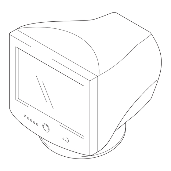
Dell P992 Service Manual
17.32 inches
Hide thumbs
Also See for P992:
- Quick setup manual (4 pages) ,
- Quick setup manual (54 pages) ,
- Service manual (75 pages)
Table of Contents
Advertisement
Quick Links
SERVICE MANUAL
Screen dimensions
Preset Image Size
4:3
Viewable Image Size (VIS)
Aperture Grille Pitch
Deflection angle
Faceplate coating
Resolution
Horizontal scan range
Vertical scan range
Optimal preset resolution
Highest preset resolution
Highest addressable resolution*
* Addressable means the monitor will sync up to this mode. However, Dell
does not guarantee the image will be sized and centered correctly.
Dell guarantees image size and centering for all preset modes listed in the
following table.
Electrical
Video input signals
Synchronization input signals
SPECIFICATIONS
Diagonal 17.32 inches (440 mm)
Horizontal 13.86 inches (352 mm)
Vertical 10.39 inches (264 mm)
Diagonal 17.97 inches (456.4 mm)
Horizontal 14.37 inches (365 mm)
Vertical 10.79 inches (274 mm)
0.24 - 0.25 mm
90°
AR Coating
30 kHz to 107 kHz (automatic)
48 Hz to 170 Hz (automatic)
1024 x 768 at 85 Hz
1600 x 1200 at 85 Hz
1920 x 1200 at 75 Hz
Analog, 0.7 Vpp, positive at 75 ohm
Separate horizontal and vertical; and
composite TTL level, positive or
negative Sync on Green at 0.3 Vp-p
Canadian Model
N. Hemisphere Model
S. Hemisphere Model
Equator Model
Chinese Model
AC input voltage / frequency /
current
Inrush current at 120 V
Inrush current at 240 V
Physical Characteristics
Connector type
Signal cable type
Dimensions:
Height
Width
Depth
Weight (monitor only)
Weight (with packaging)
Environmental
Temperature:
Operating
Nonoperating
Humidity:
Operating
Nonoperating
Altitude:
Operating
Nonoperating
Thermal dissipation
P992 COLOR MONITOR
P992
US Model
Chassis No. SCC-L42A-A
AEP Model
Chassis No. SCC-L42E-A
Japan Model
Chassis No. SCC-L42B-A
CRV
CHASSIS
100 to 240 VAC / 50 or 60 Hz ± 3 Hz /
2.0 A (RMS) at 120 VAC and
1.0 A (RMS) at 220 VAC
50 A
80 A
15-pin D-subminiature
Attached to monitor
471 mm (18.54 inches)
451 mm (17.76 inches)
461 mm (18.15 inches)
25.5 kg (56.1 lb)
30.0 kg (66.0 lb)
32° to 104°F (0° to 40°C)
-4° to 140°F (-20° to 60°C)
10% to 80% (noncondensing)
5% to 90% (noncondensing)
3,048 m (10,000 ft)
10,675 m (35,000 ft)
461 BTU/hour (maximum)
427 BTU/hour (typical)
R
Advertisement
Table of Contents

Summary of Contents for Dell P992
-
Page 1: Service Manual
1920 x 1200 at 75 Hz Temperature: Operating 32° to 104°F (0° to 40°C) * Addressable means the monitor will sync up to this mode. However, Dell Nonoperating -4° to 140°F (-20° to 60°C) does not guarantee the image will be sized and centered correctly. - Page 2 T503 OP1+ Q506 HSHAPE :LCT OP2+ REFDC Hdrive REFDC T509 HD OUT HD OUT :HCC H DY HFBP H.LINBAL H LIN BAL SW HFBP Q510 D.TILT D.TILT S501 (RASTER CENTER TAP SWITCH) LCC NS LCC NS B-SS9330<U/C>-BD3-EPS05 P992 (E) 4-3...
-
Page 3: Hv Regulator Circuit Check
Check T901 (FBT) Source Transistor Drain (FET) Gate • Mounted D Board Emitter Transistor Collector N Board IC1001, RB1001 Base – • Mounted N Board Discrete semiconductot Ver.1.6 (Chip semiconductors that are not actually used are included.) P992 (E) 4-7... -
Page 4: Schematic Diagram Of A Board
TO D-b BOARD TO D-c BOARD CN1102 CN604 TO D-b BOARD • A BOARD WAVEFORMS 0.74 Vp-p (H) 1.03 Vp-p (H) 54.0 Vp-p (H) 52.8 Vp-p (H) 0.73 Vp-p (H) 53.6 Vp-p (H) 5.1 Vp-p (24.5 MHz) P992 (E) 4-8... -
Page 5: Schematic Diagrams Of D (A, B, C) Board
R755 8.2k B:CHIP :RN-CP R567 R566 R565 R564 R563 :CHIP :CHIP :CHIP :CHIP :CHIP :CHIP :CHIP :CHIP :CHIP :CHIP :CHIP :CHIP :CHIP :CHIP :CHIP :CHIP :CHIP :CHIP :CHIP :CHIP :CHIP :CHIP :CHIP :CHIP :CHIP :CHIP -a(DEFLECTION) B-SSS9330<U/C>-D..-P1-EPS05 P992 (E) 4-10... - Page 6 :MPS R954 R919 C921 R920 D912 C923 R923 0.47 RD15ES-T1B3 :CHIP :CHIP :RN-CP F:CHIP C938 Q907 2SB709A R921 ABL DET 4.7k G2 MUTE R955 C929 :CHIP CN904 CN1102 CN510 TO A1 BOARD TO A BOARD CN318 CN311 P992 (E) 4-11...
- Page 7 :SURGE :SURGE :SURGE 0.0022 FH601 D628 250V F601 1SS133T-77 AC IN 6.3A R675 AC L JW(5) Q608 FH602 DTC143ESA-TP SG603 11.8 RELAY AC N DRIVE TH601 DGS SW ADA_3.3V 200V CN601 B-SSS9330<U/C>-D..-P3-EPS05 CN604 TO A BOARD CN312 P992 (E) 4-12...
-
Page 8: Schematic Diagram Of Da Board
1.6k :CHIP :RN-CP :CHIP :CHIP A.GND :CHIP C1133 C1132 220 4V :CHIP 0.01 B:CHIP PLL LOCK HD OUT C1138 D1105 A.GND 100p H FBP STZ6.8 CH:CHIP A.GND A.GND V.DF D1107 H.DF STZ6.8 TO D-a BOARD CN502 B-SS9330<U/C>-DA..-P1-EPS05 P992 (E) 4-14... - Page 9 S1401 S1400 LED 2 CN1103 MENU CONT- BRT+ C1498 CHASSIS GND R1421 Q1400 DTC114ESA-TP LED DRIVE FB1404 R1419 TH1400 R1424 R1406 100k Q1401 R1420 C1407 R1407 DTC114TSA D1403 LED DRIVE RD5.1ESB POWER D1400 SML79423C-TP15 (USER CONTROL) B-SS9330<U/C>-H4..-EPS05 P992 (E) 4-16...
-
Page 10: Schematic Diagram Of N Board
DDC GND2 47 :CHIP DDC SDA DSCL2 HV DET DSDA2 ECO SW DSCL1 R1040 DSDA1 100 :CHIP IIC SCL R1017 1k :CHIP IIC SDA R1016 TO D- a BOARD R1043 R1044 100 :CHIP CN1104 :CHIP :CHIP B-SS9330<U/C>-N..-EPS05 P992 (E) 4-18...


Need help?
Do you have a question about the P992 and is the answer not in the manual?
Questions and answers