Table of Contents
Advertisement
Quick Links
Download this manual
See also:
Owner's Manual
Advertisement
Table of Contents

Related Manuals for Emerson EWD7002


Summary of Contents for Emerson EWD7002
- Page 1 SERVICE MANUAL DVD PLAYER EWD7002...
-
Page 2: Table Of Contents
IMPORTANT SAFETY NOTICE Proper service and repair is important to the safe, reliable operation of all Funai Equipment. The service procedures recommended by Funai and described in this service manual are effective methods of performing service operations. Some of these service special tools should be used when and as recommended. - Page 3 Manufactured under license from Dolby Laboratories. "Dolby" and the double-D symbol are trademarks of Dolby Laboratories. "DTS" and "DTS Digital Out" are trademarks of Digital Theater Systems Inc.
-
Page 4: Specifications
SPECIFICATIONS ITEM CONDITIONS UNIT NOMINAL LIMIT 1. Video Output 75 ohm load 2. Coaxial Digital Out mVpp 3. Audio (PCM) 3-1. Output Level 1kHz 0dB Vrms 3-2. S/N 3-3. Freq. Response fs=48kHz 20~22kHz ± 2 fs=44.1kHz 20~20 kHz ± 2 3-4. -
Page 5: Laser Beam Safety Precautions
LASER BEAM SAFETY PRECAUTIONS This DVD player uses a pickup that emits a laser beam. Do not look directly at the laser beam coming from the pickup or allow it to strike against your skin. The laser beam is emitted from the location shown in the figure. When checking the laser diode, be sure to keep your eyes at least 30cm away from the pickup lens when the diode is turned on. -
Page 6: Important Safety Precautions
IMPORTANT SAFETY PRECAUTIONS Product Safety Notice I. Also check areas surrounding repaired locations. J. Be careful that foreign objects (screws, solder Some electrical and mechanical parts have special droplets, etc.) do not remain inside the set. safety-related characteristics which are often not evi- K. -
Page 7: Safety Check After Servicing
Safety Check after Servicing Examine the area surrounding the repaired location for damage or deterioration. Observe that screws, parts, Chassis or Secondary Conductor and wires have been returned to their original posi- tions. Afterwards, do the following tests and confirm the specified values to verify compliance with safety Primary Circuit Terminals standards. -
Page 8: Standard Notes For Servicing
STANDARD NOTES FOR SERVICING Circuit Board Indications How to Remove / Install Flat Pack-IC a. The output pin of the 3 pin Regulator ICs is indi- 1. Removal cated as shown. With Hot-Air Flat Pack-IC Desoldering Machine:. (1) Prepare the hot-air flat pack-IC desoldering Top View Bottom View machine, then apply hot air to the Flat Pack-IC... - Page 9 With Soldering Iron: (4) Bottom of the flat pack-IC is fixed with glue to the CBA; when removing entire flat pack-IC, first apply (1) Using desoldering braid, remove the solder from all soldering iron to center of the flat pack-IC and heat pins of the flat pack-IC.
- Page 10 Instructions for Handling 2. Installation Semi-conductors (1) Using desoldering braid, remove the solder from the foil of each pin of the flat pack-IC on the CBA Electrostatic breakdown of the semi-conductors may so you can install a replacement flat pack-IC more occur due to a potential difference caused by electro- easily.
-
Page 11: Operating Controls And Functions
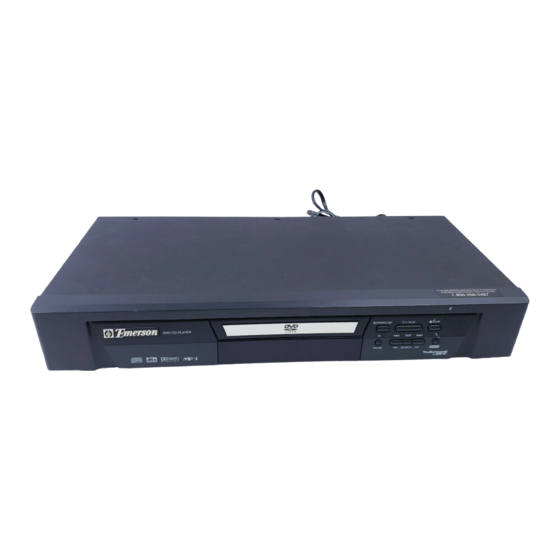
OPERATING CONTROLS AND FUNCTIONS FRONT PANEL OPEN/CLOSE PLAY STOP SKIP PAUSE SEARCH POWER 10. SKIP DOWN Button (remote control) REMOTE CONTROL Plays back from the beginning of the current chapter or track. 11. OPEN/CLOSE Button Press to insert discs into or remove them from the tray. SEARCH OPEN/ POWER... -
Page 12: Rear View
REAR VIEW COAXIAL AUDIO OUT VIDEO S-VIDEO 32 33 34 35 36 37 31. Power Cord 35. VIDEO OUT Jack 32. COAXIAL DIGITAL AUDIO OUT Jack 36. Component Video Out Jacks 33. Right AUDIO OUT Jack 37. S-VIDEO OUT Jack 34. -
Page 13: Cabinet Disassembly Instructions
CABINET DISASSEMBLY INSTRUCTIONS 1. Disassembly Flowchart (1): Identification (location) No. of parts in the figures (2): Name of the part This flowchart indicates the disassembly steps to gain (3): Figure Number for reference access to item(s) to be serviced. When reassembling, (4): Identification of parts to be removed, unhooked, follow the steps in reverse order. - Page 14 (S-1) DVD Mecha [1] Top Cover (S-1) Short the three short lands by soldering (S-1) Fig. D1 Tray Panel (L-2) (L-1) (L-1) View for A Short the three short lands by soldering Slide [2] Front Assembly (L-3) Fig. D2 Pickup Unit View for C (S-2) View for B...
- Page 15 (S-6) [4] AV CBA (S-4) CN1601 [6] Rear Panel CN1001 (S-5) (S-4) (S-3) (S-3) Fig. D6 [5] DVD Main CBA Unit Fig. D5 HOW TO MANUAL EJECT 1. Remove the Top Case. 2. Insert the eject-bar (length = approximately 80 mm, diameter = approximately 3 mm) into the manual eject hole on the DVD Mecha.
-
Page 16: Block Diagrams
BLOCK DIAGRAMS System Control Block Diagram IC601 (DVD HOST PROCESSOR) IC301 TFWD (FRONT END PROCESSOR) TREV TFWD TOUT TFWD TREV TREV TOUT IC605 TOUT +3.3V STDIO RESET RESET FROM/TO STDIO RF SIGNAL PROCESS MUTE HANG 46 MUTE /SERVO Q701 47 PS BLOCK DIAGRAM CD/DVD... - Page 17 RF Signal Process/Servo Block Diagram DATA(VIDEO/AUDIO) SIGNAL FOCUS SERVO SIGNAL TRACKING SERVO SIGNAL SLIDE SERVO SIGNAL DISK SERVO SIGNAL IC101 (RF SIGNAL PROCESS) PICK-UP UNIT DVD MAIN CBA UNIT HOLD TESTSG CN101 FROM/TO DVD SIGNAL PROCESS BLOCK DIAGRAM NARF C 10 DETECTOR BDO DET INPUT...
- Page 18 DVD Signal Process Block Diagram DATA(VIDEO/AUDIO) SIGNAL DVD MAIN CBA UNIT IC201 (DVD SIGNAL PROCESS) PARA0 PARA1 PARA2 DATA VIDEO/AUDIO PARA3 SLICER PARA0-PARA7 TO VIDEO DEMODULATOR FROM/TO RF SIGNAL INTERFACE NARF PARA4 BLOCK DIAGRAM PROCESS/SERVO PARA5 BLOCK DIAGRAM TESTSG PARA6 PARA7 MEMORY MANAGER...
-
Page 19: Video Block Diagram
Video Block Diagram DATA(VIDEO) SIGNAL DATA(AUDIO) SIGNAL VIDEO SIGNAL DATA(VIDEO/AUDIO) SIGNAL IC601 (DVD HOST PROCESSOR) CACHE SUBSYSTEM FROM DVD PARA0 INTERNAL CENTRAL FRONT-END PCM-BCK SIGNAL PROCESS PARA0-PARA7 PERIPHERALS COMMAND & LINK PCM-DATA0 BLOCK DIAGRAM PARA7 TO AUDIO PORTS PORT INTERFACE PCM-SCLK BLOCK AUDIO... -
Page 20: Audio Block Diagram
Audio Block Diagram DATA(AUDIO) SIGNAL AUDIO SIGNAL WF 6 JK1202 CN701 CN1601 Q1351 SPDIF DIGITAL AUDIO OUT IC801 (AUDIO DAC) IC1201 (AMP) SPDIF CN701 CN1601 4X/8X L-CH PCM-BCK AUDIO-L ENPHANCED LPF+AMP AUDIO-L OVERSAMPLING PCM-DATA0 SERIAL MULTI-LEVEL AUDIO-R DIGITAL FILTER PORT PCM-LRCLK DELTA-SIGMA /FUNCTION... -
Page 21: Power Supply Block Diagram
Power Supply Block Diagram CAUTION ! CAUTION Switching power supply circuit is used in this unit. FOR CONTINUED PROTECTION AGAINST FIRE HAZARD, NOTE : If Main Fuse (F1001) is blown, check to see that all components in the REPLACE ONLY WITH THE SAME TYPE FUSE. The voltage for parts in hot circuit is measured using power supply circuit are not defective before you connect the AC plug to ATTENTION : POUR UNE PROTECTION CONTINUE LES RISQES... -
Page 22: Schematic Diagrams / Cba's And Test Points
SCHEMATIC DIAGRAMS / CBA’S AND TEST POINTS Standard Notes Notes: WARNING 1. Do not use the part number shown on these draw- ings for ordering. The correct part number is Many electrical and mechanical parts in this chassis shown in the parts list, and may be slightly different have special characteristics. - Page 23 LIST OF CAUTION, NOTES, AND SYMBOLS USED IN THE SCHEMATIC DIAGRAMS ON THE FOLLOWING PAGES: 1. CAUTION: FOR CONTINUED PROTECTION AGAINST FIRE HAZARD, REPLACE ONLY WITH THE SAME TYPE FUSE. ATTENTION: POUR UNE PROTECTION CONTINUE LES RISQES D'INCELE N'UTILISER QUE DES FUSIBLE DE MEMO TYPE.
- Page 24 DVD Main 1/4 Schematic Diagram DATA(VIDEO+AUDIO) FOCUS SERVO SIGNAL TRACKING SERVO SIGNAL MAIN 1/4 Ref No. Position IC101 IC102 IC103 IC301 TRANSISTORS Q101 Q102 CONNECTORS CN101 CN302 CN501 1-8-3 1-8-4 E5662SCD1 1-8-5...
- Page 25 DVD Main 2/4 Schematic Diagram DATA(VIDEO+AUDIO) FOCUS SERVO SIGNAL TRACKING SERVO SIGNAL SPINDLE SERVO SIGNAL SLIDE SERVO SIGNAL MAIN 2/4 Ref No. Position IC201 IC401 TRANSISTORS Q401 CONNECTORS CN201 CN401 1-8-6 1-8-7 1-8-8 E5662SCD2...
- Page 26 DVD Main 3/4 Schematic Diagram DATA(VIDEO+AUDIO) DATA(VIDEO) VIDEO SIGNAL DATA(AUDIO) MAIN 3/4 Ref No. Position IC601 IC602 IC605 IC606 TRANSISTORS Q701 1-8-9 1-8-10 1-8-11 E5662SCD3...
- Page 27 DVD Main 4/4 Schematic Diagram VIDEO SIGNAL DATA(AUDIO) AUDIO SIGNAL MAIN 4/4 Ref No. Position IC604 IC801 CONNECTOR CN701 AA-2 E5662SCD4 AV 1/3 Schematic Diagram AV 1/3 NOTE : Ref No. Position The voltage for parts in hot circuit is measured using hot GND as a common terminal.
- Page 28 AV 2/3 Schematic Diagram AV 2/3 Ref No. Position IC1201 IC1402 VIDEO SIGNAL TRANSISTORS Q1201 DATA(AUDIO) Q1202 Q1203 AUDIO SIGNAL Q1204 Q1351 CONNECTORS CN1601 1-8-15 1-8-16 E5662SCAV2...
- Page 29 AV 3/3 & Function Schematic Diagram FL2001 MATRIX CHART STANDBY STANDBY TITLE CHP. TRK. REPEAT REPEAT TITLE CHP. TRK. AV 3/3 Ref No. Position IC2001 1-8-17 1-8-18 E5662SCAV3...
- Page 30 AV CBA Top View CAUTION ! Switching power supply circuit is used in this unit. If Main Fuse (F1001) is blown, check to see that all components in the power supply circuit are not defective before you connect the AC plug to the AC power supply.
-
Page 31: Av Cba Bottom View
AV CBA Bottom View CAUTION ! Switching power supply circuit is used in this unit. PIN 5 OF PIN 7 OF PIN 9 OF PIN 13 OF PIN 15 OF PIN 18 OF If Main Fuse (F1001) is blown, check to see that all components in the CN1601 CN1601 CN1601... -
Page 32: Waveforms
WAVEFORMS Pin 5 of CN1601 Pin 15 of CN1601 NOTE: Input CD: 1kHz PLAY (WF4~WF6) DVD: POWER ON (STOP) MODE (WF1~WF3) VIDEO-Y 0.2V 20usec AUDIO-R 0.5msec Pin 7 of CN1601 Pin 18 of CN1601 VIDEO-CVBS 0.5V 20usec SPDIF 0.2usec Pin 9 of CN1601 VIDEO-C 0.2V 20usec... -
Page 33: Wiring Diagram
WIRING DIAGRAM VIDEO-Y VIDEO-U VIDEO-V VIDEO AUDIO AUDIO DIGITAL S-VIDEO AC CORD OUT(L) OUT(R) AUDIO OUT AV CBA (BE5600F01013-A) CN1001 CN1601 CN501 CN701 DVD MAIN CBA UNIT CN302 CN101 CN201 CN401 (NO CONNECTION) (NO CONNECTION) LOADING MOTOR SENSOR TRAY-OUT TRAY-IN FG CBA SPINDLE SW CBA... -
Page 34: Rom Renewal Mode
ROM RENEWAL MODE 1. Turn the power on and remove the disc on the tray. 2. To put the DVD player into version up mode, press [9], [8], [7], [6], and [SEARCH MODE] buttons on the remote control unit in that order. The tray will open automatically. -
Page 35: System Control Timing Charts
SYSTEM CONTROL TIMING CHARTS Tray close ~ Play / Play ~ Tray open Eject key on Eject key on Tray close Play Tray open Disc Rotation LSW2 LSW1 4.4s (TL123) 700ms 2.0s 1.2s ( TP122 ) 1.7s ( TL122 ) 1-12-1 DVDTI... -
Page 36: Ic Pin Function Descriptions
IC PIN FUNCTION DESCRIPTIONS IC2001 [ PT6315-S/ PT6315-S(-TP) ] Signal In/Out Name Function Name Clock Input Serial Interface Strobe Key Data 1 Input Key Data 2 Input Power Supply a / KEY-1 Segment Output / Key Source-1 Segment Output / Key b / Key-2 Source-2 Segment Output / Key... -
Page 37: Lead Identifications
LEAD IDENTIFICATIONS 2SK3374 2SC2785 (H) 2SA1015-Y (TPE2) KTC3199 (GR) KTA1266 (Y) KRA110M 2SA966 (Y) KTA1273 (Y) 2SC2236-Y-TPE6,C KRC110M-AT BA1L3Z-T BN1L3Z (P) KTC3205 (Y) G D S E C B E C B PT6315-S NJM4558D MM1567AJ PT6315-S(-TP) KIA431-AT KIA4558P MM1566AF PQ018EF01SZ R A K LTV-817(B,C)-F Note:... -
Page 38: Exploded Views
EXPLODED VIEWS Cabinet 2L011 2L011 See Electrical Parts List for parts with this mark. Some Ref. Numbers are not in sequence. 2L021 2L021 2L021 2L031 2L011 W1601 JK1401 JK1403 DVD Main W1001 CBA Unit JK1201 2L031 F1001 AC1001 2L031 AV CBA 2L031 2L071 2L071... - Page 39 Packing Unit 1-15-2 E5662EX...
-
Page 40: Mechanical Parts List
LABEL, MODEL NO. E5662UD --------- LABEL, BAR CODE HB400UD or 0VM412678 LABEL, BAR CODE E5662UD 0VM413321 LABEL, TELEPHONE NUMBER 0VM411684 H7931UD(EMERSON) DVD MECHA 0838 VCDVM030 N79F1FVM 2L011 SCREW, C-TIGHT M3X5 BIND HEAD + GBKC3050 2L021 SCREW, S-TIGHT M3X10 BIND HEAD+... -
Page 41: Electrical Parts List
ELECTRICAL PARTS LIST PRODUCT SAFETY NOTE: Products marked with a Ref. No. Description Part No. # have special characteristics important to safety. C1038 ELECTROLYTIC CAP. 470µF/6.3V M CE0KMASDL471 Before replacing any of these components, read care- C1039 ELECTROLYTIC CAP. 47µF/16V M CE1CMASDL470 fully the product safety notice in this service manual. - Page 42 Ref. No. Description Part No. Ref. No. Description Part No. D1001 RECTIFIER DIODE 1N4005 or NDQZ001N4005 PHOTOCOUPLER LTV-817C-F NPEC0LTV817F RECTIFIER DIODE 1N4005 ND8Z001N4005 IC1002# 1.8V REGULATOR PQ018EF01SZ QSZBA0SSH012 D1002 RECTIFIER DIODE 1N4005 or NDQZ001N4005 IC1003 IC KIA431-AT NSZLA0TJY001 RECTIFIER DIODE 1N4005 ND8Z001N4005 IC1006 IC KIA431-AT...
- Page 43 Ref. No. Description Part No. Ref. No. Description Part No. CARBON RES. 1/4W J 1k Ω METAL OXIDE FILM RES. 2W J 10 Ω R1008 RCX4JATZ0102 RN02100KE009 CARBON RES. 1/6W J 15k Ω or R1010 RCX6JATZ0153 R1075 PCB JUMPER D0.6-P5.0 JW5.0T CARBON RES.
- Page 44 Ref. No. Description Part No. Ref. No. Description Part No. CHIP RES.(1608) 1/16W J 33k Ω CHIP RES.(1608) 1/10W 0 Ω or RRXGJR5Z0333 R2059 RRXAZR5Z0000 CHIP RES.(1608) 1/10W J 39k Ω or CHIP RES.(1608) 1/16W 0 Ω R1247 RRXAJR5Z0393 RRXGZR5Z0000 CHIP RES.(1608) 1/16W J 39k Ω...
- Page 45 Printed in Japan 2002-03-22 HO...
Need help?
Do you have a question about the EWD7002 and is the answer not in the manual?
Questions and answers