Table of Contents
Advertisement
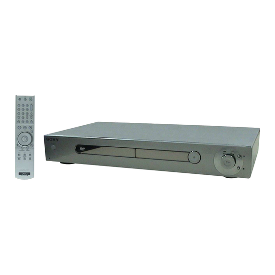
SERVICE MANUAL
System
Laser: Semiconductor laser
Signal format system: PAL (NTSC)
Audio characteristics
Frequency response: DVD VIDEO (PCM
96 kHz): 2 Hz to 44 kHz ( 1.0 dB)/DVD
VIDEO (PCM 48 kHz): 2 Hz to 22 kHz
( 0.5 dB)/CD: 2 Hz to 20 kHz ( 0.5 dB)
Signal-to-noise ratio (S/N ratio): 115 dB
(LINE OUT L/R (AUDIO) jacks only)
Harmonic distortion: 0.003 %
Dynamic range: DVD VIDEO: 103 dB/CD:
99 dB
Wow and flutter: Less than detected value
( 0.001% W PEAK)
The signals from LINE OUT L/R (AUDIO)
jacks are measured. When you play PCM
sound tracks with a 96 kHz sampling
frequency, the output signals from the
DIGITAL OUT (OPTICAL or COAXIAL)
jack are converted to 48 kHz sampling
frequency.
SPECIFICATIONS
Outputs
(Jack name: Jack type/Output level/Load
impedance)
LINE OUT (AUDIO): Phono jack/2 Vrms/
10 kilohms
DIGITAL OUT (OPTICAL): Optical
output jack/ 18 dBm (wave length
660 nm)
DIGITAL OUT (COAXIAL): Phono jack/
0.5 Vp-p/75 ohms
LINE OUT (VIDEO): Phono jack/1.0 Vp-p/
75 ohms
S VIDEO OUT: 4-pin mini DIN/Y:
1.0 Vp-p, C: 0.3 Vp-p (PAL), 0.286 Vp-p
(NTSC)/75 ohms
COMPONENT VIDEO OUT (Y, C
Phono jack/Y: 1.0 Vp-p, C
, C
B
0.7 Vp-p/75 ohms
DVP-LS500
General
Power requirements:
220 240 V AC, 50/60 Hz
Power consumption: 14 W
Dimensions (approx.):
430 × 65 × 242 mm (width/height/depth)
incl. projecting parts
Mass (approx.): 2.2 kg
Operating temperature: 5 °C to 35 °C
Operating humidity: 25 % to 80 %
Supplied accessories
Check that you have the following items:
Audio/video cord
(pinplug × 3 y pinplug × 3) (1) (UK)
, C
):
Remote commander (remote) (1)
B
R
:
Size AA (R6) batteries (2)
R
Specifications and design are subject to
change without notice.
CD/DVD PLAYER
RMT-D162P
AEP Model
UK Model
Russian Model
Advertisement
Table of Contents

Subscribe to Our Youtube Channel
Related Manuals for Sony DVP-LS500


Summary of Contents for Sony DVP-LS500
- Page 1 DVP-LS500 RMT-D162P SERVICE MANUAL AEP Model UK Model Russian Model SPECIFICATIONS System Outputs General (Jack name: Jack type/Output level/Load Laser: Semiconductor laser Power requirements: impedance) Signal format system: PAL (NTSC) 220 240 V AC, 50/60 Hz LINE OUT (AUDIO): Phono jack/2 Vrms/...
- Page 2 IC pins, etc. OPERATION. REPLACE THESE COMPONENTS WITH • Usable with ordinary solder SONY PARTS WHOSE PART NUMBERS APPEAR AS It is best to use only unleaded solder but unleaded solder may SHOWN IN THIS MANUAL OR IN SUPPLEMENTS PUB- also be added to ordinary solder.
-
Page 3: Table Of Contents
TABLE OF CONTENTS Section Title Page Section Title Page Service Note ................4 POWER SUPPLY BLOCK (ETXNY410E0F) Printed Wiring Board ............. 4-41 GENERAL POWER SUPPLY BLOCK (ETXNY410E0F) Schematic Diagram ............4-43 Index to Parts and Controls .......... 1-1 IC PIN FUNCTION DESCRIPTION Hookups ................ -
Page 4: Service Note
SERVICE NOTE 1. DISC REMOVAL PROCEDURE (at POWER OFF) 1) Open dust cover to access to a hole insert a tapering driver into the aperture of the unit bottom, and move the lever of chuck cam in the direction of arrow A. (See Fig. 1) 2) Draw out the tray in the direction of arrow B, and remove a disc. - Page 5 4) Set the board in the place where the MB-108 board is removed, as shown in Fig. 4. Flexible flat cable (FMM-48: CN105) Flexible flat cable (FMS-23: CN103) Flexible flat cable (FMO-8: CN101) CK-120 board Connector (CN113) Two screws Two screws (B3) (B3) Connector...
-
Page 6: General
DVP-LS500 SECTION 1 This section is extracted from instruction GENERAL manual (3-083-624-11). MP3 format that conforms to ISO9660* software producers. Since this player plays About this Manual This Player Can Play the Level 1/Level 2, or its extended format, DVDs and VIDEO CDs according to the disc... - Page 7 Rear panel Remote 1 TV [/1 (on/standby) button (61) (open/close) button (27) 3 Number buttons (30) DIGITAL OUT LINE OUT S VIDEO COMPONENT VIDEO OUT LINE (RGB) -TV The number 5 button has a tactile dot.* PCM/DTS/MPEG/ 4 CLEAR button (35) DOLBY DIGITAL 5 ./>...
-
Page 8: Hookups
PROGRAM (page 35) Selects the title, chapter, or track to play in the order you want. Hookups SHUFFLE (page 36) Hooking Up the Player Plays the title, chapter, or track in random order. REPEAT (page 37) Follow steps 1 to 6 to hook up and adjust the settings of the player. Plays the entire disc (all titles/all tracks/all albums) repeatedly or one title/chapter/ track/album repeatedly. - Page 9 When connecting to a standard 4:3 screen TV Step 4: Connecting the Audio Cords Depending on the disc, the image may not fit your TV screen. If you want to change the aspect ratio, please refer to page 64. Refer to the chart below to select the connection that best suits your system. Be sure to also read Notes the instructions for the components you wish to connect.
- Page 10 Connecting to an AV amplifier (receiver) having a Dolby Surround (Pro Connecting to an AV amplifier (receiver) with a digital input jack having Logic) decoder and 3 to 6 speakers a Dolby Digital, MPEG audio or DTS decoder and 6 speakers This connection will allow you to use the Dolby Digital, MPEG audio, or DTS decoder function You can enjoy the Dolby Surround effects only when playing Dolby Surround audio or multi- of your AV amplifier (receiver).
-
Page 11: Playing Discs
Press X/x to select whether or Press A on the player, and place a disc on the disc tray. not you wish to send a DTS signal Playing Discs to your amplifier (receiver). Playing Discs Choose the item that matches the audio connection you selected on pages 21 to 23 ( through... - Page 12 Press X/x to select the setting. Notes Using the DVD’s Menu Selecting “ORIGINAL” or PLAY LIST: plays the titles created MULTI-DISC RESUME in CUSTOM SETUP must be set to ON (default) for this from ORIGINAL for editing. “PLAY LIST” on a DVD- function to work (page 65).
- Page 13 See the instructions of the CD-R/CD-RW When you insert a DATA CD and press H, 1 2 ( 2 7 ) Various Play Mode device or recording software (not supplied) the numbered tracks are played sequentially, 1 8 ( 3 4 ) DVD VIDEO for details on the recording format.
-
Page 14: Searching For A Scene
◆ When playing a VIDEO CD or CD Press X/x to select (A-B To return to normal play DISC: repeats all of the tracks. REPEAT), then press ENTER. Press CLEAR, or select OFF in step 3. TRACK: repeats the current track. The options for A-B REPEAT ◆... -
Page 15: Viewing Information About The Disc
◆ When playing a VIDEO CD with PBC To turn off the Control Menu z Hint Playback Searching by Scene Yo u can also select PICTURE NAVIGATION Press DISPLAY repeatedly until the Control from the Control Menu (page 12). SCENE Menu is turned off. -
Page 16: Sound Adjustments
To turn off the Control Menu Checking the play information of Checking the Play Press DISPLAY repeatedly until the Control a DATA CD Menu is turned off. Information By pressing TIME/TEXT while playing MP3 Display of each item audio tracks on a DATA CD, you can display By pressing DISPLAY repeatedly, you can You can check information such as the bit the audio bit rate (the amount of data per... -
Page 17: Enjoying Movies
R: right) without using actual rear speakers. L: Front speaker (left) between the front L and R speakers is short, TVS was developed by Sony to produce R: Front speaker (right) such as with built-in speakers on a stereo TV. -
Page 18: Using Various Additional Functions
further increasing the picture contrast C 0 1 : 3 2 : 5 5 Adjusting the Playback Enhancing the Playback and the colour intensity. CINEMA 1: enhances details in dark PICTURE Picture Picture (CUSTOM PICTURE MODE) BRIGHTNESS (DIGITAL VIDEO areas by increasing the black level. COLOR CINEMA 2: White colours become ENHANCER) - Page 19 2047 You can control the sound level, input source, If your TV is listed in the table below, set the Press X/x to select and power switch of your Sony TV with the Austria 2046 appropriate manufacturer s code. (PARENTAL CONTROL), then press supplied remote.
-
Page 20: Settings And Adjustments
Press X/x to select “CUSTOM,” Selected setting Setting the Display or then press ENTER. SCREEN SETUP Settings and Adjustments TV TYPE: 4:3 PAN SCAN Sound Track Language The Setup Display appears. SCREEN SAVER: BACKGROUND: JACKET PICTURE Using the Setup Display LANGUAGE SETUP LINE: VIDEO... -
Page 21: Additional Information
, AUTO PLAY in CUSTOM SETUP is any problem persist, consult your nearest The disc does not play. set to ON (page 65). Sony dealer. Sound , The disc is turned over. Insert the disc with the playback side facing Power There is no sound. -
Page 22: Language Code List
DVD VIDEO. number is digital. The DVD-RW has two different modes: VR , Contact your Sony dealer or local mode and Video mode. DVD-RWs created in authorized Sony service facility. C 13 The disc is dirty. -
Page 23: Disassembly
DVP-LS500 SECTION 2 DISASSEMBLY 2-1. DISASSEMBLY • This set can be disassembled in the order shown below. Upper case (Page 2-1) Tray panel MB-108 board (Page 2-2) (Page 2-4) Front panel section (Page 2-2) Mechanism deck Power block AF-98 board... -
Page 24: Tray Panel
2-3. TRAY PANEL 1 Open the dust cover. 5 Tray panel 2 Slide the lever. 4 Two claws 3 Draw out the tray. 2-4. FRONT PANEL SECTION 3 Claw 2 Claw 4 Claw 1 Flexible flat cable 5 Claw (FFS-10: CN402) 6 Claw 7 Front panel section... -
Page 25: Mechanism Deck
2-5. MECHANISM DECK 5 Three screws (B3) 1 Connector (CN201) 6 Mechanism deck 2 Connector (CN471) 3 Two flexible flat cables (FMO-8: CN203/FMS-23: CN204) 4 Flexible flat cable (FMM-48: CN201) 2-6. OPTICAL PICK-UP 7 Insulator 3 Insulator screw 5 Insulator 4 Optical pick-up 6 Insulator 1 Insulator screw... -
Page 26: Board
2-7. ER-26 BOARD 3 ER-26 board 1 Flexible flat cable (FAE-9: CN901) 2 Two screws (B3) 2-8. MB-108 BOARD 4 Flexible flat cable (FMM-48: CN201) 3 Two flexible flat cables (FMO-8: CN203/FMS-23: CN204) 8 Screw (B3) 7 Screw (B3) 5 Connector 1 Connector (CN102) (CN601) -
Page 27: Power Block
2-9. POWER BLOCK 3 Four screws (B3) 1 Connector (CN101) 2 Connector (CN201) 4 Power block 2-10. AF-98 BOARD 2 Connector (CN471) 4 Two screws 1 Flexible flat cable (B3) (FAE-9: CN102) 5 AF-98 board 3 Seven screws (B3) -
Page 28: Internal Views
2-11. INTERNAL VIEWS — Top view — — Bottom view — M001 Loading motor 1-763-967-11 Optical pick-up (KHM-290AAA) A-6061-908-A... -
Page 29: Circuit Boards Location
2-12. CIRCUIT BOARDS LOCATION ER-26 board Power supply block (EURO AV) (ETXNY410E0F) AF-98 board (INTERFACE CONTROL AUDIO/VIDEO OUT) MS-128 board (LOADING MOTOR) MB-108 board (SIGNAL PROCESS SERVO) SW-384 board (FUNCTION SWITCH) 2-7 E... -
Page 30: Block Diagrams
DVP-LS500 SECTION 3 BLOCK DIAGRAMS 3-1. OVERALL BLOCK DIAGRAM MB-108 BOARD AF-98 BOARD (SEE PAGE 4-9 to 4-22) (SEE PAGE 4-27 to 4-34) IC404 IC405 16M SDRAM J103 S VIDEO OUT V, Y, C V, Y, C IC303 BASE UNIT... -
Page 31: Rf/Servo Block Diagram
DVP-LS500 3-2. RF/SERVO BLOCK DIAGRAM IC201 tl (DVD play) IC201 tl (CD play) IC201 1 (DVD play) IC201 1 (CD play) IC201 rs (DVD play) IC201 rs (CD play) 500 mV/DIV 100 ns/DIV 500 mV/DIV 200 ns/DIV 500 mV/DIV 100 ns/DIV... -
Page 32: Signal Processor Block Diagram
DVP-LS500 3-3. SIGNAL PROCESSOR BLOCK DIAGRAM MB-108 BOARD (2/4) (SEE PAGE 4-11 to 4-14) IC404, 405 16M SDRAM IC303 16M DRAM IC301 <zzz (DVD play) 105 – 108·110 – 113· 135 – 138·140 – 143· 121·122·124· 500 mV/DIV 100 ns/DIV IC403 tj 115·116·118·120... -
Page 33: System Control Block Diagram
DVP-LS500 3-4. SYSTEM CONTROL BLOCK DIAGRAM MB-108 BOARD (3/4) (SEE PAGE 4-17, 19) IC108 IC106 IC107 1M SRAM 32M FLASH HA 0 – 21 HA 0 – 21 HD 0 – 15 HD 0 – 15 IC104 td 1 – 5 102 – 109 111 – 118 120 85 – 100 59 72 84 3.2 Vp-p (16.5 MHz) -
Page 34: Video Block Diagram
DVP-LS500 3-5. VIDEO BLOCK DIAGRAM IC102 wl AF-98 BOARD (1/3) (LINE : S VIDEO mode) IC102 ed (SEE PAGE 4-27) IC102 VIDEO BUFFER 2.4 Vp-p (H) 2.0 Vp-p (H) J104 (1/2) CN203 (1/2) VIDEO IN VIDEO OUT VIDEO LINE OUT... -
Page 35: Audio Block Diagram
DVP-LS500 3-6. AUDIO BLOCK DIAGRAM AF-98 BOARD (2/3) (SEE PAGE 4-29) MB-108 BOARD (4/4) IC601 2 IC601 4 (SEE PAGE 4-21) IC204 D IN OPTICAL DVD: 3.8 Vp-p (3.1 MHz) DVD: 3.6 Vp-p (48 kHz) CD: 3.8 Vp-p (2.8 MHz) CD: 3.6 Vp-p (44.1 kHz) -
Page 36: Interface Control Block Diagram
DVP-LS500 3-7. INTERFACE CONTROL BLOCK DIAGRAM AF-98 BOARD (3/3) (SEE PAGE 4-33) CN401 SW-384 BOARD (SEE PAGE 4-36) SYSTEM CONTROL XIFCS XIFCS (SEE PAGE 3-8) XIFBUSY IC820 XIFBUSY BUSY REMOTE COMMANDER RECEIVER CN402 CN801 S801 S802 S803 S816 S805 VOUT... -
Page 37: Power 1 Block Diagram
DVP-LS500 3-8. POWER 1 BLOCK DIAGRAM POWER SUPPLY BLOCK (ETXNY410E0F) (SEE PAGE 4-43) CN201 Q301 L301 D301 SW+11V • T101 L205 D201 L201 EVER+11V Q203 D202 F201 L202 SW+5V CN101 D104-D107 AC IN F101 L101, 102 LINE FILTER Q204 D203... -
Page 38: Power 2 Block Diagram
DVP-LS500 3-9. POWER 2 BLOCK DIAGRAM ER-26 BOARD AF-98 BOARD (SEE PAGE 4-39) (SEE PAGE 4-27 to 4-34) IC902 CN471 PS472 CN102 CN901 -5V REG IC901 EVER+11V +11V +11V VIDEO -15V BUFFER, Q472, 473 PS471 SELECT IC103 L905 SWITCH EVER-15.5V... -
Page 39: Printed Wiring Boards And Schematic Diagrams
DVP-LS500 SECTION 4 PRINTED WIRING BOARDS AND SCHEMATIC DIAGRAMS For schematic diagram: THIS NOTE IS COMMON FOR PRINTED WIRING • Caution when replacing chip parts. BOARDS AND SCHEMATIC DIAGRAMS. New parts must be attached after removal of chip. Be careful not to heat the minus side of tantalum capacitor, For printed wiring boards: because it is damaged by the heat. -
Page 40: Frame Schematic Diagram
DVP-LS500 4-1. FRAME SCHEMATIC DIAGRAM CN102 21P CN901 21P CNJ902 GND(E) -15V -15V V_IN V/Y_OUT D_GND_VIDEO D_GND_VIDEO GND(E) GND(E) D_GND_VIDEO D_GND_VIDEO BLANKING_OUT R/C_OUT D_GND_VIDEO D_GND_VIDEO GND(E) Cb/R_Cb/B Cb/R_Cb/B GND(E) D_GND_VIDEO D_GND_VIDEO N.C. ER-26 BOARD LINE Cr/B_Cr/R Cr/B_Cr/R G_OUT (FAE-9) (RGB)-TV... -
Page 41: Printed Wiring Boards And Schematic Diagrams
DVP-LS500 4-2. PRINTED WIRING BOARDS AND SCHEMATIC DIAGRAMS There are a few cases that the part isn't mounted in this model is printed on this diagram. MB-108 (SIGNAL PROCESS, SERVO) PRINTED WIRING BOARD – Ref. No.: MB-108 board; 2,000 series –... - Page 42 DVP-LS500 MB-108 BOARD (SIDE B) MB-108 BOARD(SIDE B) IC101 IC103 IC505 IC106 IC108 IC201 IC202 R577 IC503 C538 IC303 C518 IC401 R417 C243 Q202 IC404 R436 R416 C602 L202 IC405 C429 C415 IC406 Q201 C439 R522 JL505 R526 Q202 FL403...
-
Page 43: Rf Amp, Servo) Schematic Diagram
DVP-LS500 The components identified by mark 0 or dotted MB-108 (RF AMP, SERVO) SCHEMATIC DIAGRAM • See page 4-5 for printed wiring board. line with mark 0 are critical for safety. – Ref. No.: MB-108 board; 2,000 series – Replace only with part number specified. -
Page 44: Arp, Servo Dsp) Schematic Diagram
DVP-LS500 MB-108 (ARP, SERVO DSP) SCHEMATIC DIAGRAM • See page 4-5 for printed wiring board. – Ref. No.: MB-108 board; 2,000 series – R360 SDI0 MB-108 BOARD (2/7) SDI0 XRST MB-108 BOARD (5/7) SDI1 SDI1 SDEF SDI2 SDEF XX MARK:NO MOUNT... -
Page 45: Mb-108 (Av Decoder) Schematic Diagram
DVP-LS500 MB-108 (AV DECODER) SCHEMATIC DIAGRAM • See page 4-5 for printed wiring board. • See page 4-15 for Waveforms. – Ref. No.: MB-108 board; 2,000 series – MB-108 BOARD (3/7) NO MARK:DVD/CD PLAY D:DVD PLAY XX MARK:NO MOUNT C:CD PLAY... -
Page 46: Motor Drive) Schematic Diagram
DVP-LS500 MB-108 (MOTOR DRIVE) SCHEMATIC DIAGRAM • See page 4-5 for printed wiring board. – Ref. No.: MB-108 board; 2,000 series – MB-108 BOARD (4/7) XX MARK:NO MOUNT NO MARK:DVD/CD PLAY D:DVD PLAY C:CD PLAY +3.3V MB-108 BOARD R259 (6/7) -
Page 47: Mb-108 (System Control) Schematic Diagram
DVP-LS500 MB-108 (SYSTEM CONTROL) SCHEMATIC DIAGRAM • See page 4-5 for printed wiring board. – Ref. No.: MB-108 board; 2,000 series – MB-108 BOARD (5/7) XX MARK:NO MOUNT NO MARK:DVD/CD PLAY FL106 +3.3V MB-108 BOARD (6/7) IC106 HA16 HA17 HA15... -
Page 48: Clock Generator) Schematic Diagram
DVP-LS500 MB-108 (CLOCK GENERATOR) SCHEMATIC DIAGRAM • See page 4-5 for printed wiring board. – Ref. No.: MB-108 board; 2,000 series – • Waveforms 1 IC103 3 MB-108 BOARD (6/7) FSEL MB-108 BOARD (5/7) R116 R176 XX MARK:NO MOUNT 27MAVD... -
Page 49: Audio D/A Converter) Schematic Diagram
DVP-LS500 MB-108 (AUDIO D/A CONVERTER) SCHEMATIC DIAGRAM – Ref. No.: MB-108 board; 2,000 series – R612 MB-108 BOARD (7/7) COMPOUT FB602 COUT FB603 XX MARK:NO MOUNT YOUT R609 NO MARK:DVD/CD PLAY MB-108 BOARD R608 D:DVD PLAY (3/7) CB/R R607 C:CD PLAY... -
Page 50: Loading Motor) Printed Wiring Board And Schematic Diagram
DVP-LS500 MS-128 (LOADING MOTOR) PRINTED WIRING BOARD AND SCHEMATIC DIAGRAM – Ref. No.: MS-128 board; 1,000 series – : Uses unleaded solder. There are a few cases that the part isn't mounted in this model is printed on this diagram. -
Page 51: Interface Control Audio/Video Out) Printed Wiring Board
DVP-LS500 DIGITAL OUT COMPONENT AF-98 (INTERFACE CONTROL AUDIO/VIDEO OUT) PRINTED WIRING BOARD LINE OUT VIDEO OUT OPTICAL COAXIAL AUDIO VIDEO – Ref. No.: AF-98 board; 1,000 series – S VIDEO AF-98 BOARD : Uses unleaded solder. J104 J201 J103 JL204... -
Page 52: Af-98 (Video Out) Schematic Diagram
DVP-LS500 AF-98 (VIDEO OUT) SCHEMATIC DIAGRAM • See page 4-25 for printed wiring board. – Ref. No.: AF-98 board; 1,000 series – AF-98 BOARD (1/4) XX MARK:NO MOUNT NO MARK:DVD/CD PLAY R125 JL136 LCH_OUT V_MUTE JL118 L101 AF-98 BOARD AF-98 BOARD (4/4) -
Page 53: Af-98 (Audio Out) Schematic Diagram
DVP-LS500 AF-98 (AUDIO OUT) SCHEMATIC DIAGRAM • See page 4-25 for printed wiring board. – Ref. No.: AF-98 board; 1,000 series – SIGNAL PATH AF-98 BOARD (2/4) VIDEO SIGNAL AUDIO XX MARK:NO MOUNT SIGNAL NO MARK:DVD/CD PLAY CHROMA Y/CHROMA R201 4700 0.5%... -
Page 54: Regulator) Schematic Diagram
DVP-LS500 AF-98 (REGULATOR) SCHEMATIC DIAGRAM • See page 4-25 for printed wiring board. – Ref. No.: AF-98 board; 1,000 series – AF-98 BOARD (3/4) XX MARK:NO MOUNT IC473 NO MARK:DVD/CD PLAY +1.8V REG IC473 LMS8117ADTX-1.8/NOPB C488 C487 C489 C485 FB471 SW+1.8V... -
Page 55: If Con) Schematic Diagram
DVP-LS500 AF-98 (IF CON) SCHEMATIC DIAGRAM – Ref. No.: AF-98 board; 1,000 series – MB-108 BOARD (6/7) MB-108 BOARD (6/7) CN102 CN101 DOWNLOAD • Waveforms AF-98 BOARD (4/4) (SEE PAGE 4-20) (SEE PAGE 4-20) (JIG) XX MARK:NO MOUNT 1 IC404 3 NO MARK:DVD/CD PLAY ∗:IMPOSSIBLE TO MEASURE THE... -
Page 56: Function Switch) Printed Wiring Board And Schematic Diagram
DVP-LS500 SW-384 (FUNCTION SWITCH) PRINTED WIRING BOARD AND SCHEMATIC DIAGRAM – Ref. No.: SW-384 board; 1,000 series – : Uses unleaded solder. There are a few cases that the part isn't mounted in this model is printed on this diagram. -
Page 57: Euro Av) Printed Wiring Board
DVP-LS500 ER-26 (EURO AV) PRINTED WIRING BOARD – Ref. No.: ER-26 board; 1,000 series – : Uses unleaded solder. LINE (RGB) -TV There are a few cases that the part isn't mounted in this model is printed on this diagram. -
Page 58: Euro Av) Schematic Diagram
DVP-LS500 ER-26 (EURO AV) SCHEMATIC DIAGRAM • Waveforms – Ref. No.: ER-26 board; 1,000 series – 1 IC901 ef (LINE : RGB mode) ER-26 BOARD IC902 -5V REG XX MARK:NO MOUNT IC902 L79M05TLL-SONY-TL NO MARK:DVD/CD PLAY R920 R921 SIGNAL PATH -11.2... -
Page 59: Power Supply Block (Etxny410E0F) Printed Wiring Board
DVP-LS500 POWER SUPPLY BLOCK (ETXNY410E0F) PRINTED WIRING BOARD – Ref. No.: ETXNY410E0F board; 3,000 series – : Uses unleaded solder. There are a few cases that the part isn't mounted in this model is printed on this diagram. POWER SUPPLY BLOCK... -
Page 60: Power Supply Block (Etxny410E0F) Schematic Diagram
DVP-LS500 POWER SUPPLY BLOCK (ETXNY410E0F) SCHEMATIC DIAGRAM – Ref. No.: ETXNY410E0F board; 3,000 series – POWER SUPPLY BLOCK (ETXNY410E0F) -REF.NO.:3000 SERIES- XX MARK:NO MOUNT NO MARK:PB MODE 10.3 B+ SWITCH 10.5 2A/250V EVER+11V B+ SWITCH AC IN 311.5 AF-98 BOARD (3/4) -
Page 61: Ic Pin Function Description
DVP-LS500 SECTION 5 IC PIN FUNCTION DESCRIPTION... - Page 62 5-2 E...
-
Page 63: Test Mode
DVP-LS500 SECTION 6 TEST MODE 6-1. GENERAL DESCRIPTION 6-3. SYSCON DIAGNOSIS The Test Mode allows you to make diagnosis and adjustment eas- The same contents as board detail check by serial interface can be ily using the remote commander and monitor TV. The instructions, checked from the remote commander. - Page 64 * In "All item continuous check", pressing stop or enter will not (2-6) M't check quit the diagnosis. Mount resistance is checked. Error 22: The region code does not accord. Selecting 2 and subsequent items calls the submenu screen of Check wether the region code that is deduced from model each item.
- Page 65 5. Data Supply System (5-5) ARP RAM Check (5-2) ARP Register Check Data write → read, and accord check Data write → read, and accord check Error 11: ARP RAM read data discord Error 08: ARP register write, and read data discord The program code data stored in ROM are copied to all Data 0x00 to 0xFF is written sequentially to the ARP TMAX areas of RAM (IC303) connected to the ARP (IC301)
- Page 66 7. Video Output Diagnosis Check Items List (7-2) Color Bar AVD color bar command write → Video OUT 2) Version Error: Not detected. (2-2) Revision The command is transferred to the AVD, and the color bar (2-3) ROM Check Sum signals are output from video terminals.
- Page 67 Error Codes List 00: Error not detected 01: RAM write/read data discord 03: EEPROM NG 04: Flash memory clear error 05: Flash memory write error 06: Flash memory read data discord 08: ARP register read data discord 09: ARP ←→ RAM data bus error 10: ARP ←→...
-
Page 68: Drive Auto Adjustment
1. DVD Single Layer Disc 6-4. DRIVE AUTO ADJUSTMENT [ENTER] Select , insert DVD single layer disc, and press key, and the adjustment will be made through the following steps, then DVD reference disc adjusted values will be written to the EEPROM. Single Layer HLX-503 (J-6090-069-A) (NTSC) DVD Single Layer Disc Adjustment Steps... - Page 69 2. CD 3. DVD Dual Layer Disc [ENTER] [ENTER] Select , insert CD disc, and press key, and the adjust- Select , insert DVD dual layer disc, and press key, ment will be made through the following steps, then adjusted val- and the adjustment will be made through the following steps, then ues will be written to the EEPROM.
-
Page 70: Drive Manual Operation
0. Disc Check Memory 6-5. DRIVE MANUAL OPERATION Disc Check On the Test Mode Menu screen, select , and the manual opera- tion menu will be displayed. For the manual operation, each servo on/off control and adjustment can be executed manually. 1. - Page 71 Focus : Search the focus and turn on the focus. Disc Type 1. Disc Type Auto Check 2. DVD SL 12cm : Turn ON/OFF the tracking servo. 3. DVD DL 12cm 4. CD 12cm Sled : Turn ON/OFF the sled servo. 5.
- Page 72 5. Auto Adjustment ← Fj (L0 → L1) : Focus jump reverse. (Trk/Sled Servo OFF) Auto Adjustment ↑ Lj (L1 → L0) : Layer jump forward. 1. Auto TRK. Offset 2. Auto FCS Balance (Trk/Sled Servo ON) 3. Auto Focus Offset 4.
-
Page 73: Mecha Aging
6-7. EMERGENCY HISTORY EEPROM Data 3 -– DL -– CD LCD Analog FRSW xx xx ### EMG. History ### PLL Dac Gain xx xx Mirror Time xx xx Laser Hours xxhxxm TRK. Balance xxhxxm THR A&L: xx xx xx/xx xx 1. -
Page 74: Version Information
6-8. VERSION INFORMATION 6-10. IF CON SELF DIAGNOSTIC FUNCTION 1. AF-98 BOARD (IF CON) TEST MODE ### Version Infomation ### The AF-98 board (IF CON) test mode is the IF CON self diagnos- IF con. Ver:x.xxx(xxxx) tic mode. The IF CON can diagnose the functions of the AF-98 Group board that the IF CON controls. - Page 75 2-2. Operation of Auto Self Check When the Self Check mode becomes active at the AC Power ON or by key input, the test display of the following steps (1) to (4) is repeated. (1) FLD and LED all ON (for 5 seconds) (2) MODEL display (for 2 seconds) (3) Version display (for 2 seconds) (4) ROM creation date display (for 2 seconds)
- Page 76 2-3. Each Self Check Function Each Self Check function tests the FLD display, LED display, and key input. IC404: Pin No. (Signal) Input Voltage [V] Pin ef (AD1) Pin eg (O/C) Pin eh (AD2) Pin ej (POWER) 0 – 0.21 PLAY OPEN/CLOSE –...
- Page 77 Key code display (at input of key, Key code: 0Ah) At input of faulty voltage When key is pressed double 2-3-3. Remote Commander Key Name Display and Key Code Display 2-3-3-1. Transition Keys in Self Check Mode • Remote commander keys except keys transited in Self Check Mode 2-3-3-2.
- Page 78 2-3-4. Communication Monitoring Display The communication state is monitored and displayed while the key name on the main unit and the remote commander is displayed. When the communication to the System Controller failed, DVD and VCD segments turn on. Communication error display (at no input of key and remote com- mander) Communication error display (at code display without input of the remote commander)
- Page 79 2-3-6. FLD Grid Test Display and SHUTTLE Click Operation Test 2-3-6-1. Transition Keys in Self Check Mode • Key on the remote commander ↑ • SHUTTLE on the remote commander during Grid Test display 2-3-6-2. Operation and Display The Self Check Mode transits to this mode when key is en- ↑...
- Page 80 (7G-1G) ANODE CONNECTION 6-18...
-
Page 81: Troubleshooting
1-3. Clock signal check 6-11. TROUBLESHOOTING Measure the clock signal frequency at CPUCK (CL101) of 6-11-1. Cannot Enter Test Mode SYSCON (IC104) with an oscilloscope. You cannot enter the Test mode when either button has been pressed If the 8.25 MHz signal appears. t Check the machine ac- by any reason with the board assembled in the front panel. - Page 82 1-3-2. When the 33 MHz signal appears at CPUCK 3. If the message “SDSP No Ack” appears after the menu • WAIT signal check is displayed. 3-1. ARP & SERVO clock signal check Observe XWAIT (pin-yj) of SYSCON (IC104) with an os- cilloscope.
- Page 83 6-11-3. Drive Auto Adjustment stops due to error. 2-2. Check XFRRST (pin-8) at CN101 on the MB-108 The ARP & SERVO (IC301) analog circuit of MB-108 board is board. If it is fixed to “L”. t The signal line has defective solder- defective or RF-Amp (IC201) or M-Driver (IC202) peripheral cir- cuit is defective or optical pickup block is defective or flat cable ing, or is short-circuited with other signal lines, or parts are...
-
Page 84: Electrical Adjustment
DVP-LS500 SECTION 7 ELECTRICAL ADJUSTMENT 7-1. POWER SUPPLY CHECK In making adjustment, refer to 7-6. Adjustment Related Parts Arrangement. 1. ETXNY410E0F Board Note: During diagnostic check, the characters and color bars can Mode be seen only with the NTSC monitor. Therefore, for diag-... -
Page 85: Adjustment Of Video System
7-2. ADJUSTMENT OF VIDEO SYSTEM 3. Checking S Video Output S-C <Purpose> This checks whether the S video output S-C satisfies the NTSC/ 1. Video Level Adjustment (MB-108 BOARD) PAL Standard. If it is not correct, the colors will be too dark or <Purpose>... -
Page 86: Checking Component Video Output B-Y
5. Checking Component Video Output B-Y 7. Checking RGB Output R <Purpose> <Purpose> This checks component video output B-Y. If it is incorrect, cor- This checks RGB output R. If it is incorrect, pictures will not be rect colors will not be displayed when connected to, for instance, displayed correctly in spite of connection to the TV with an EURO component input projector. -
Page 87: Checking Rgb Output B
9. Checking RGB Output B <Purpose> This checks RGB output B. If it is incorrect, pictures will not be displayed correctly in spite of connection to the TV with an EURO AV connecting cord. Mode Play Signal Check the Color-bar (100%) signal on DVD reference disc Test point LINE (RGB)-TV connector... -
Page 88: Adjustment Related Parts Arrangement
7-3. ADJUSTMENT RELATED PARTS ARRANGEMENT MB-108 BOARD (SIDE A) VIDEO LEVEL ADJ RV401 IC403 ETXNY410E0F BOARD (SIDE A) CN201 7-6 E... -
Page 89: Repair Parts List
DVP-LS500 SECTION 8 REPAIR PARTS LIST 8-1. EXPLODED VIEWS NOTE: • -XX and -X mean standardized parts, so they may • The mechanical parts with no reference number in The components identified by mark have some difference from the original one. -
Page 90: Chassis Section
8-1-2. CHASSIS SECTION supplied supplied supplied The components identified by mark 0 or dotted line with mark 0 are critical for safety. Replace only with part number speci- fied. Ref. No. Part No. Description Remark Ref. No. Part No. Description Remark 0 51 1-468-744-11 POWER SUPPLY BLOCK... -
Page 91: Mechanism Deck Assembly
8-1-3. MECHANISM DECK ASSEMBLY supplied supplied supplied supplied supplied M001 supplied supplied supplied supplied supplied The components identified by mark 0 or dotted line with mark 0 are critical for safety. Replace only with part number speci- fied. Ref. No. Part No. -
Page 92: Electrical Parts List
AF-98 8-2. ELECTRICAL PARTS LIST NOTE: The components identified by mark • Due to standardization, replacements in the • Items marked “*” are not stocked since they 0 or dotted line with mark 0 are parts list may be different from the parts speci- are seldom required for routine service. - Page 93 AF-98 Ref. No. Part No. Description Remark Ref. No. Part No. Description Remark IC201 6-701-937-01 IC TJM4558CDT < FLUORESCENT INDICATOR > IC203 8-759-711-59 IC NJM78L05UA-TE1 IC204 6-600-185-01 IC GP1FA553TZ0F (DIGITAL OUT OPTICAL) ND401 1-518-876-11 VACUUM FLUORESCENT DISPLAY IC404 6-802-768-01 IC 86CK74AFG-4H19 (M) <...
- Page 94 < IC > R447 1-216-025-11 RES-CHIP 1/10W R453 1-218-616-91 METAL CHIP IC901 8-759-826-47 IC LA73052-TLM R457 1-218-628-11 METAL CHIP IC902 8-759-667-17 IC L79M05TLL-SONY-TL R458 1-218-628-11 METAL CHIP R459 1-216-298-00 METAL CHIP 1/10W < JUMPER RESISTOR > R460 1-216-073-91 RES-CHIP 1/10W JR901...
- Page 95 ER-26 MB-108 Ref. No. Part No. Description Remark Ref. No. Part No. Description Remark < COIL > C120 1-162-970-11 CERAMIC CHIP 0.01uF C121 1-162-970-11 CERAMIC CHIP 0.01uF L905 1-412-064-11 INDUCTOR 100uH C122 1-162-970-11 CERAMIC CHIP 0.01uF C125 1-126-607-11 ELECT CHIP 47uF <...
- Page 96 MB-108 Ref. No. Part No. Description Remark Ref. No. Part No. Description Remark C263 1-124-779-00 ELECT CHIP 10uF C420 1-107-826-11 CERAMIC CHIP 0.1uF C264 1-117-863-11 CERAMIC CHIP 0.47uF 6.3V C422 1-162-970-11 CERAMIC CHIP 0.01uF C265 1-107-826-11 CERAMIC CHIP 0.1uF C423 1-162-970-11 CERAMIC CHIP 0.01uF C266...
- Page 97 MB-108 Ref. No. Part No. Description Remark Ref. No. Part No. Description Remark IC202 6-701-878-01 IC FAN8034L R166 1-216-295-91 SHORT CHIP IC301 6-701-876-01 IC CXD9703R R168 1-216-827-11 METAL CHIP 3.3K 1/10W IC302 6-702-302-01 IC TK11133CSCL-G R169 1-216-089-91 RES-CHIP 1/10W IC303 6-703-843-01 IC GLT4161L16P-50TCT (AEP, UK) R169...
- Page 98 MB-108 MS-128 SW-384 Ref. No. Part No. Description Remark Ref. No. Part No. Description Remark R259 1-216-833-11 METAL CHIP 1/10W R423 1-216-833-11 METAL CHIP 1/10W R260 1-216-834-11 METAL CHIP 1/10W R426 1-216-833-11 METAL CHIP 1/10W R261 1-216-833-11 METAL CHIP 1/10W R430 1-216-797-11 METAL CHIP 1/10W...
- Page 99 SW-384 POWER SUPPLY BLOCK (ETXNY410E0F) Ref. No. Part No. Description Remark Ref. No. Part No. Description Remark R820 1-216-017-91 RES-CHIP 1/10W R821 1-216-097-11 RES-CHIP 100K 1/10W < SWITCH > S801 1-762-875-21 SWITCH, TACT (H) S802 1-762-875-21 SWITCH, TACT (.) S803 1-762-875-21 SWITCH, TACT (>) S805 1-762-875-21 SWITCH, TACT (x)
- Page 100 DVP-LS500 Sony Corporation 2003G0500-1 9-929-759-11 Home Storage Company © 2003. 7 – 142 – Published by Customer Support Dept.
Need help?
Do you have a question about the DVP-LS500 and is the answer not in the manual?
Questions and answers