Sony DVP-NS999ES Service Manual
Hide thumbs
Also See for DVP-NS999ES:
- Operating instructions manual (96 pages) ,
- Specifications (2 pages) ,
- Technical details (53 pages)
Table of Contents
Advertisement
Quick Links
SERVICE MANUAL
System
Laser: Semiconductor laser
Signal format system:
NT
SC: US, CND
PAL/(NTSC): AEP, UK, KR
Audio characteristics
Frequency response: DVD VIDEO (PCM
96 kHz): 2 Hz to 44 kHz (44 kHz: –2 dB
±1 dB), Super Audio CD: 2 Hz to
100 kHz (50 kHz: –3 dB ±1 dB), CD:
2 Hz to 20 kHz (±0.5 dB)
Harmonic distortion: DVD VIDEO/Super
Audio CD: 0.0012 %, CD: 0.0016 %
Dynamic range: DVD VIDEO/Super Audio
CD: 103 dB, CD: 99 dB
Wow and flutter: Less than detected value
(±0.001% W PEAK)
Outputs
(Jack name: Jack type/Output level/Load
impedance)
AUDIO OUT 1/2: Phono jack/2 Vrms/
10 kilohms
DIGITAL OUT (OPTICAL): Optical
output jack/–18 dBm (wave length:
660 nm)
DIGITAL OUT (COAXIAL): Phono jack/
0.5 Vp-p/75 ohms
5.1CH OUTPUT: Phono jack/2 Vrms/
10 kilohms
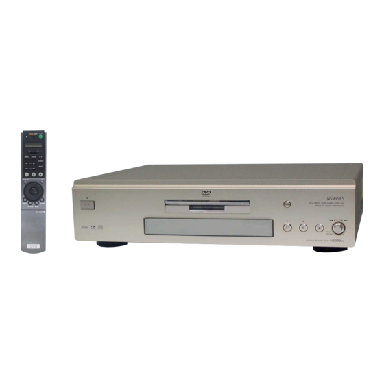
DVP-NS999ES
Photo: Gold type
SPECIFICATIONS
COMPONENT VIDEO OUT(Y, P
Phono jack/Y: 1.0 Vp-p/P
, P
B
interlace*=0.648 Vp-p, progressive or
interlace**=0.7 Vp-p/75 ohms
* BLACK LEVEL is ON
** BLACK LEVEL is OFF
VIDEO OUT 1/2: Phono jack/1.0 Vp-p/
75 ohms
S VIDEO OUT 1/2: 4-pin mini DIN/Y:
1.0 Vp-p, C: 0.286 Vp-p/75 ohms
General
Power requirements:
120 V AC, 60 Hz (US, CND)
220 V – 240 V AC, 50/60 Hz
(AEP, UK, KR)
Power consumption:
20 W (US, CND)
23 W (AEP, UK, KR)
Dimensions (approx.):
430 × 113 × 349 mm (17 × 4
in.) (width/height/depth) incl. projecting
parts
Mass (approx.):6.4 kg (14 lb 2 oz)
Operating temperature: 5 °C to 35 °C
(41 °F to 95 °F)
Operating humidity: 25 % to 80 %
RMT-D150A/D150P
Canadian Model
Korean model
Supplied accessories
, P
):
B
R
:
Check that you have the following items:
R
• Audio/video cord (pinplug × 3 y pinplug
× 3) (1)
• Power cord (1)
• Remote commander (remote) (1)
• Siz
e AA (R6) batteries (2)
Specifications and design are subject to
change without notice.
• Abbreviation
CND : Canadian
KR : Korea
1
/
× 13
3
/
2
4
CD/DVD PLAYER
US Model
AEP Model
UK Model
Advertisement
Table of Contents


Need help?
Do you have a question about the DVP-NS999ES and is the answer not in the manual?
Questions and answers