Table of Contents
Advertisement
Quick Links
SERVICE MANUAL
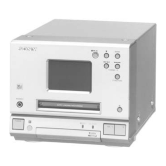
HMD-M11 is the mini disc deck,
tuner and preamplifier section
in CMT-M11C.
U.S and foreign patents licensed from Dolby Labora-
tories Licensing Corporation.
MiniDisc deck section
System
MiniDisc digital audio system
Disc
MiniDisc
Laser
Semiconductor laser (λ = 780 nm)
Laser output power
Less than 44.6 mW*
* This output is the value measured at a distance of 200 mm from the ob-
jective lens surface on the optical pick-up block with 7 mm aperture.
Laser diode properties
Material: GaAlAs
Revolutions (CLV)
Approx. 400 rpm to 900 rpm
Error correction
Advanced Cross
Interleave Reed Solomon Code (ACIRC)
Sampling frequency
44.1 kHz
Modulation system
EFM (Eight-to-Fourteen Modulation)
Number of channels
2 stereo channels
Frequency response
20 to 20,000 Hz ± 0.5 dB
Signal-to-noise ratio
Over 92 dB (during playback)
Wow and flutter
Below measurable limit
Inputs
DIGITAL IN (CD OPTICAL IN):
Square optical connector jack, impedance opti-
cal wave length 660 nm.
MICROFILM
HMD-M11
Model Name Using Similar Mechanism
MD Mechanism Type
Optical Pick-up Name
SPECIFICATIONS
Tuner section
Tuning range
US, CND model
AEP, UK model
E, HK, SP, MY model
Intermediate frequency
Antenna terminals
Timer
Timer setting
Sleep timer
MINI DISC DECK/TUNER/PREAMPLIFIER
US Model
Canadian Model
AEP Model
UK Model
E Model
NEW
MDM-3C
KMS-260A/J1N
FM: 87.5 – 108 MHz
(100 kHz step)
AM: 530 – 1,710 kHz
(at 10 kHz interval)
FM: 87.5 – 108 MHz
(50 kHz step)
AM: 522 – 1,611 kHz
FM: 87.5 – 108 MHz
(50 kHz step)
AM: 531 – 1,602 kHz
(at 9 kHz interval)
530 – 1,710 kHz
(at 10 kHz interval)
FM: 10.7 MHz
AM: 450 kHz
FM: 75 ohm unbalanced
AM: External antenna terminal
Quartz lock system
One-minute step
10-minute step, max. 90 minutes
– Continued on next page –
Advertisement
Table of Contents

Related Manuals for Sony HMD-M11


Summary of Contents for Sony HMD-M11
- Page 1 US Model SERVICE MANUAL Canadian Model AEP Model UK Model E Model HMD-M11 is the mini disc deck, tuner and preamplifier section in CMT-M11C. U.S and foreign patents licensed from Dolby Labora- Model Name Using Similar Mechanism tories Licensing Corporation.
-
Page 2: Table Of Contents
Preamplifier section TABLE OF CONTENTS Inputs TAPE IN jack: Stereo phone jacks, sensitivity 220 mV, imped- SERVICING NOTES ance 47 kilohms 1-1. Check Mode of Fluorescent Indicator Tube, Outputs OUTPUT jack: Buttons, and LED’s ............5 Stereo phone jacks, 1 V, 1 kilohm 1-2. - Page 3 SUR LES DIAGRAMMES SCHÉMATIQUES ET LA LISTE DES PIÈCES SONT CRITIQUES POUR LA SÉCURITÉ DE FONCTIONNEMENT. NE REMPLACER CES COM- POSANTS QUE PAR DES PIÈCES SONY DONT LES NUMÉROS SONT DONNÉS DANS CE MANUEL OU DANS LES SUPPLÉMENTS PUBLIÉS PAR SONY.
- Page 4 CAUTION NOTES ON HANDLING THE OPTICAL PICK-UP Danger of explosion if battery is incorrectly replaced. BLOCK OR BASE UNIT Replace only with the same or equivalent type recommended by The laser diode in the optical pick-up block may suffer electro- the manufacturer.
-
Page 5: Servicing Notes
SECTION 1 SERVICING NOTES 1-1. CHECK MODE OF FLUORESCENT INDICATOR 1-2. CHECK MODE OF AMPLIFIER SECTION TUBE, BUTTONS, AND LED’S Setting the Check Mode: This mode is activated if pressing FUNCTION button Setting the Check Mode: This mode is activated if pressing = 0 button and DISPLAY and YES button simultaneously with the power supply to the set in ON status. - Page 6 SECTION 2 This section is extracted from instruction manual. GENERAL – 6 –...
- Page 7 – 7 –...
- Page 8 – 8 –...
- Page 9 – 9 –...
- Page 10 – 10 –...
- Page 11 – 11 –...
- Page 12 – 12 –...
- Page 13 – 13 –...
- Page 14 – 14 –...
- Page 15 – 15 –...
- Page 16 – 16 –...
- Page 17 – 17 –...
- Page 18 – 18 –...
- Page 19 – 19 –...
- Page 20 – 20 –...
- Page 21 – 21 –...
- Page 22 – 22 –...
-
Page 23: Disassembly
SECTION 3 DISASSEMBLY • This set can be disassembled in the order shown below. COVER, FRONT PANEL SECTION PRE BOARD POWER BOARD (Page 23) (Page 24) (Page 24) MECHANISM DECK SECTION SHIELD CASE (UPPER) (Page 25) (Page 25) SHIELD CASE (LOWER), BRACKET (MDM) (Page 26) BD BOARD SUB CHASSIS... - Page 24 PRE BOARD 1 two screws (BVTT3 × 5) 5 pre board 4 wire (flat type)(27 core) (CN601) 2 three screws (BVTP3 × 10) 3 three connectors (CN602, 603, 820) POWER BOARD 1 two connectors (CN804, 807) 1 connector 2 wire (flat type) (19 core) (CN803) (CN805) 3 two screws...
- Page 25 MECHANISM DECK SECTION (MDM-3C) 1 connector (CN890) 2 screw (BVTP3 × 8) 3 Remove the mechanism deck section to direction of the arrow. 2 screw (BVTP3 × 8) 2 two screws (BVTP3 × 8) SHIELD CASE (UPPER) 1 three screws 2 bracket (ferrite) (M1.7 ×...
- Page 26 SHIELD CASE (LOWER), BRACKET (MDM) 5 sheet (flexible) 4 two rivet 7 bracket (MDM) 6 two screws (BVTT2 × 3) 2 wire (flat type) (19core) (CN100) 2 wire (flat type) (29 core) 1 two screws (CN102) (BVTT2 × 5) 1 two screws (BVTT2 ×...
- Page 27 SUB CHASSIS 1 two step screws 1 two step screws 2 insulator 2 insulator part A part A part A 3 sub chassis Take care so that the part A may be right position when installing. SHUTTER ASS’Y 1 stopper washer 2 shaft (shutter) A shutter ass’y shaft (shutter) B...
- Page 28 OVER WRITE HEAD 1 screw (P1.7 × 6) 2 over write head SLIDER COMPLETE ASS’Y claw 3 Set the shaft of gear (LB) to be at the position in the figure. claw 45° 1 special screw (M1.7 × 1.4) 2 retainer (gear) 4 Remove the slider complete ass’y in the direction of arrow with putting out of two claws.
- Page 29 NOTE FOR INSTALLATION • SLIDER COMPLETE ASS’Y slider ass’y Install the part A of lever (head up) to pass over the slider complete ass’y. part A Take care not to damage the detective switch. – 29 –...
-
Page 30: Precautions For Use Of Test Mode
SECTION 4 TEST MODE 4-1. PRECAUTIONS FOR USE OF TEST MODE 4-5. SELECTING THE TEST MODE Thirteen test modes are selected by pressing the = 0 but- 1. As loading related operations will be performed regardless of ton, and ) + button. the test mode operations being performed, be sure to check that the disc is stopped before setting and removing it. -
Page 31: Operating The Continuous Playback Mode
4-6. OPERATING THE CONTINUOUS PLAYBACK 4-7. OPERATING THE CONTINUOUS RECORDING MODE MODE 4-6-1. Entering the Continuous Playback Mode 4-7-1. Entering the Continuous Recording Mode 1. Set the disc in the unit. (Whichever recordable discs or discs 1. Set the MO disc in the unit. (Refer to note 3.) 2. -
Page 32: Eep Mode
4-8. EEP MODE 1. MODE display This mode reads and writes the contents of the non-volatile Displays “TEMP ADJUST”, “CPLAY MODE”, etc.. memory. It is not used in servicing. If set accidentally, press the NO button 2. Error rate display immediately to exit it. -
Page 33: Precautions For Checking Laser Diode Emission
SECTION 5 ELECTRICAL ADJUSTMENTS 5-3. PRECAUTIONS FOR ADJUSTMENTS 5-1. PRECAUTIONS FOR CHECKING LASER DI- 1) When replacing the following parts, perform the adjustments ODE EMISSION and checks with ® in the order shown in the following table. To check the emission of the laser diode during adjustments, never view directly from the top as this may lose your eyesight. - Page 34 5-5. TEMPERATURE COMPENSATION OFFSET 5-6. LASER POWER ADJUSTMENT ADJUSTMENT Connection: Save the temperature data at that time in the non-volatile memory laser power meter as 25°C reference data. Notes: 1. Usually, do not perform this adjustment. 2. Perform this adjustment in an ambient temperature of 22 °C to Optical pick-up 28 °C.
-
Page 35: Traverse (E-F Balance) Adjustment
5-7. TRAVERSE (E-F BALANCE) ADJUSTMENT 8. Press the = 0 button or ) + button so that the waveforms of the oscilloscope becomes the specified value. Note 1: Data will be erased during MO reading if a recorded (When the = 0 button or ) + button is pressed, disc is used in this adjustment. -
Page 36: Focus Bias Adjustment
5-8. FOCUS BIAS ADJUSTMENT 5-9. ERROR RATE CHECK Adjusting Method: 5-9-1. CD Error Rate Check 1. Load a continuously recorded disc (Refer to “5-4. Creating Checking Method: MO Continuously Recorded Disc”.). 1. Load a test disc TDYS-1. 2. Press the = 0 button or ) + button and display 2. -
Page 37: Adjusting Points And Connecting Points
SECTION 6 DIAGRAMS • Circuit Boards Location 5-11. ADJUSTING POINTS AND CONNECTING POINTS [BD BOARD] (COMPONENT SIDE) PRE board CN110 I+3V CN101 D101 POWER board IC192 SWITCH board DISPLAY board [BD BOARD] (CONDUCTOR SIDE) TRANSFORMER board POSISTOR board CONNECTOR board IC171 SW board IC101... -
Page 38: Block Diagram (1/3)
HMD-M11 6-1. BLOCK DIAGRAM (1/3) ADDT DADT HR901 OVER WRITE HEAD OVER WRITE OVER WRITE EFMO ADDT HEAD DRIVE HEAD DRIVE Q181, 182 IC181 OPTICAL WAVE SHAPER INPUT DIGITAL IN Q180 FILI DIGITAL IC380 RF AMP, IC890 FILO AUDIO FOCUS/TRACKING... -
Page 39: Block Diagram (2/3)
HMD-M11 6-2. BLOCK DIAGRAM (2/3) LINE AMP IC201 • Signal path. INLP AOUTL+ – : MD PLAY INLM ADDT ADDT I/O CIRCUIT CONVERTER (Page 43) INRP : MD REC AOUTL– CIRCUIT R-CH INRM – AINL– (REC) 10 11... -
Page 40: Block Diagram (3/3)
HMD-M11 6-3. BLOCK DIAGRAM (3/3) • Signal path. TM101 : MD PLAY ANTENNA FM-ANT : MD REC R-CH FM/AM R-CH : CD FM 75Ω FM-ANT TUNER UNIT L-CH 17 : FM TB101 : AM AM-ANT AEP, UK TM101 ANTENNA OUTPUT SELECT FM 75Ω... -
Page 41: Md Mechanism Deck Section
• Waveforms – MD MECHANISM DECK Section – 1 IC101 1, 2 (I, J) (Play Mode) 6 IC151 #¡ (CAPA+) (Play Mode) !¡ IC121 @¶ (FS256) Approx. 4.6 Vp-p 500 mVp-p 3.4 Vp-p 11.2896 MHz 1.5 µ sec !™ IC123 1 7 IC121 (º... -
Page 42: A/D, D/A Converter Section
– MECHANISM CONTROL, A/D, D/A CONVERTER Section – 1 IC100 @¶ (XOUT) 6 IC202 @∞ (512FS) 3.4 Vp-p 2.8 Vp-p 12 MHz 22.5792 MHz 2 IC100 @¢ (XOUT-T) 7 IC202 #∞ (XOUT) 1.8 Vp-p 2.5 Vp-p 22.5792 MHz 32.768 kHz 3 IC202 0, @•... -
Page 43: Master Control, Power Supply Section
– MASTER CONTROL, POWER SUPPLY Section – 1 IC700 &£ (XT1) 3 Vp-p 32.768 kHz 2 IC700 &º (X1) 4 Vp-p 5 MHz – DISPLAY Section – 1 IC901 @º (XOUT) 5 Vp-p Approx. 384 kHz 2 IC901 @¡ (XIN) 0.8 Vp-p Approx. - Page 44 – 48 –...
- Page 45 – 49 –...
- Page 46 – 50 –...
- Page 47 – 51 –...
- Page 48 – 52 –...
- Page 49 – 53 –...
- Page 50 – 54 –...
- Page 51 – 55 –...
- Page 52 – 56 –...
- Page 53 – 57 –...
- Page 54 – 58 –...
- Page 55 – 59 –...
- Page 56 – 60 –...
- Page 57 – 61 –...
- Page 58 – 62 –...
- Page 59 – 63 –...
- Page 60 – 64 –...
- Page 61 – 65 –...
- Page 62 – 66 –...
- Page 63 – 67 –...
- Page 64 – 68 –...
- Page 65 – 69 –...
- Page 66 – 70 –...
- Page 67 – 71 –...
- Page 68 – 72 –...
- Page 69 – 73 –...
- Page 70 – 74 –...
- Page 71 – 75 –...
- Page 72 – 76 –...
- Page 73 – 77 –...
- Page 74 – 78 –...
- Page 75 – 79 –...
- Page 76 – 80 –...
- Page 77 • IC Block Diagrams IC121 CXD2650R – MD MECHANISM DECK Section – IC101 CXA2523R 100 99 98 97 96 95 94 93 92 91 90 89 88 87 86 85 84 83 82 81 80 79 78 77 76 75 AUX2 SPINDLE GENERATOR SERVO...
- Page 78 – MECHANISM CONTROL, A/D, D/A CONVERTER Section – IC201 CXA8054M IC361 BA6287F OUT1 – – OUT2 DRIVER DRIVER VREF CONTROL LOGIC – – POWER SAVE IC202 CXD8607N-T6 INRP INLP MODULATOR MODULATOR INRM INLM – – REFI REFO AVDD LVSS AVSS LVDD DECIMATION DECIMATION...
-
Page 79: Master Control, Power Supply Section
– AUDIO/TUNER Section – – MASTER CONTROL, POWER SUPPLY Section – IC640 TC9210P IC820 M5293L L-CH R-CH REFERENCE DATA DATA VOLTAGE L-CH R-CH LATCH LATCH CIRCUIT CIRCUIT A-GND A-GND REFERENCE ON/OFF – VOLTAGE OVERHEAT OVERCURRENT SHIFT RESISTER PROTECTION LIMITTER LEVEL (13bit) LEVEL SHIFT... -
Page 80: Ic Pin Function Description
6-14. IC PIN FUNCTION DESCRIPTION BD BOARD IC101 CXA2523R (RF AMPLIFIER) Pin No. Pin Name I / O Function I-V converted RF signal I input from the optical pick-up block detector I-V converted RF signal J input from the optical pick-up block detector Middle point voltage (+1.65V) generation output terminal 4 to 9 A to F... - Page 81 BD BOARD IC121 CXD2650R (DIGITAL SIGNAL PROCESSOR, DIGITAL SERVO PROCESSOR, EFM/ACIRC ENCODER/DECODER, SHO PROOF MEMORY CONTROLLER, ATRAC ENCODER/DECODER, 2M BIT D-RAM) Pin No. Pin Name I / O Function Focus OK signal output to the mechanism controller (IC100) “H” is output when focus is on SHCK Track jump detection signal output to the mechanism controller (IC100) XBUSY...
- Page 82 Pin No. Pin Name I / O Function DVSS — Ground terminal (digital system) Output enable signal output to the external D-RAM Not used (open) XCAS Column address strobe signal output to the external D-RAM Not used (open) Address signal output to the external D-RAM Not used (open) XRAS Row address strobe signal output to the external D-RAM...
- Page 83 Pin No. Pin Name I / O Function TRDR Tracking servo drive PWM signal output terminal (–) TFDR Tracking servo drive PWM signal output terminal (+) DVDD — Power supply terminal (+3.3V) (digital system) FFDR Focus servo drive PWM signal output terminal (+) FRDR Focus servo drive PWM signal output terminal (–) Clock signal (176.4 kHz) output terminal (X’tal system)
- Page 84 DIGITAL BOARD IC100 RU8X12MF-0012 (MECHANISM CONTROLLER) Pin No. Pin Name I / O Function DAOUT0 Output terminal for the test C1 is output when test mode DAOUT1 Output terminal for the test ADER is output when test mode KEY0 KEY1 Key input terminal Not used (fixed at “H”) KEY2...
- Page 85 Pin No. Pin Name I / O Function LED0 LED drive signal output terminal Not used (open) — Not used (fixed at “L”) — Not used (fixed at “L”) RST-LOW Output of signal to place the reset in “L” status after a backup processing is finished —...
- Page 86 Pin No. Pin Name I / O Function Laser modulation select signal output Playback power: “L”, Stop: “H”, Recording power: 0.5 sec 2 sec REC/PB Not used (open) — Not used (open) Recording data output enable signal output to the CXD2650R (IC121) SCTX Writing data transmission timing output (Also serves as the magnetic head on/off output) XLATCH...
- Page 87 DIGITAL BOARD IC202 CXD8607N (A/D, D/A CONVERTER) Pin No. Pin Name I / O Function INRP R-ch analog signal (+) input terminal INRM R-ch analog signal (–) input terminal REFI Reference voltage (+3.3V) input terminal (for A/D converter section) AVDD —...
- Page 88 Pin No. Pin Name I / O Function VDD1 — Power supply terminal (+5V) (for A/D converter section, digital system) VSS1 — Ground terminal (for A/D converter section, digital system) TEST2 Input terminal for the test (fixed at “L”) TEST3 Input terminal for the test (fixed at “L”) VSS1 —...
- Page 89 µPD78058GC-299-3B9 (MASTER CONTROLLER) POWER BOARD IC700 Pin No. Pin Name I / O Function Not used (fixed at “L”) System reset signal output to the mechanism controller (IC100) “L”: reset MD RESET For several hundreds msec. after the power supply rises, “L” is output, then it changes to “H” Not used (fixed at “L”) AVSS —...
- Page 90 Pin No. Pin Name I / O Function DATA OUT PLL serial data output to the FM/AM (MW) tuner unit (TB101) DATA IN PLL serial data input from the FM/AM (MW) tuner unit (TB101) DBFB DBFB on/off selection signal output to the DBFB circuit “L”: DBFB on, “H”: DBFB off DBFB 1/2 mode selection signal output to the DBFB circuit DBFB 1/2...
-
Page 91: Exploded Views
Ref. No. Part No. Description Remark 4-986-543-01 PANEL (AL), FRONT * 10 A-4392-194-A DISPLAY BOARD, COMPLETE 4-942-636-21 EMBLEM (NO. 3.5), SONY * 11 1-663-485-11 SWITCH BOARD 4-975-365-01 SCREW (ALUMINUM) 4-986-551-01 BUTTON (PLAY) 4-986-546-01 INDICATOR (PLAY) X-4947-774-1 LID ASSY X-4947-787-1 PANEL ASSY, FRONT 4-986-564-01 CUSHION (FOOT) 4-951-620-01 SCREW (2.6X8), +BVTP... - Page 92 (2) CHASSIS SECTION T800 not supplied EXCEPT US, E, SP, MY Canadian US, Canadian not supplied not supplied CNJ800 not supplied not supplied The components identified by Les composants identifiés par une mark ! or dotted line with marque ! sont critiques pour la mark ! are critical for safety.
- Page 93 (3) MECHANISM DECK SECTION-1 (MDM-3C) not supplied US, Canadian, AEP, UK not supplied not supplied not supplied not supplied not supplied Ref. No. Part No. Description Remark Ref. No. Part No. Description Remark * 101 A-4699-092-A BD BOARD, COMPLETE * 109 A-4398-223-A DIGITAL BOARD, COMPLETE 4-987-736-01 SHAFT (SHUTTER) 1-782-052-11 WIRE (FLAT TYPE) (29 CORE)
- Page 94 (4) MECHANISM DECK SECTION-2 (MDM-3C) not supplied not supplied not supplied M902 M903 M901 HR901 The components identified by Les composants identifiés par une mark ! or dotted line with marque ! sont critiques pour la mark ! are critical for safety. sécurité.
-
Page 95: Electrical Parts List
SECTION 8 ELECTRICAL PARTS LIST NOTE: • Due to standardization, replacements in the • Items marked “*” are not stocked since they The components identified by mark are seldom required for routine service. ! or dotted line with mark ! are parts list may be different from the parts speci- critical for safety. - Page 96 CONNECTOR Ref. No. Part No. Description Remark Ref. No. Part No. Description Remark IC181 8-759-095-65 IC TC74ACT540FS R143 1-216-073-00 METAL CHIP 1/10W IC192 8-759-426-95 IC L88MS33T-TL R144 1-216-025-00 METAL CHIP 1/10W < COIL > R146 1-216-037-00 METAL CHIP 1/10W R147 1-216-025-00 METAL CHIP 1/10W L101...
- Page 97 CONNECTOR DIGITAL Ref. No. Part No. Description Remark Ref. No. Part No. Description Remark < IC > C254 1-163-038-00 CERAMIC CHIP 0.1uF C255 1-163-117-00 CERAMIC CHIP 100PF C256 1-163-001-11 CERAMIC CHIP 220PF 10% 50V IC890 8-749-012-70 IC GP1F38R (DIGITAL IN) C257 1-163-017-00 CERAMIC CHIP 0.0047uF 5%...
- Page 98 DIGITAL Ref. No. Part No. Description Remark Ref. No. Part No. Description Remark IC100 8-759-463-76 IC RU8X12MF-0012 R122 1-216-073-00 METAL CHIP 1/10W IC105 8-759-233-66 IC TC74HCT04AF R123 1-216-073-00 METAL CHIP 1/10W IC201 8-759-352-59 IC CXA8054M IC202 8-759-426-99 IC CXD8607N-T6 R124 1-216-073-00 METAL CHIP 1/10W R127...
- Page 99 DIGITAL DISPLAY POSISTOR POWER Ref. No. Part No. Description Remark Ref. No. Part No. Description Remark R312 1-216-017-00 METAL CHIP 1/10W < TRANSISTOR > R321 1-550-907-21 BEAD, FERRITE (CHIP) Q900 8-729-424-08 TRANSISTOR UN2111 R361 1-216-025-00 METAL CHIP 1/10W Q901 8-729-424-08 TRANSISTOR UN2111 R362 1-216-073-00 METAL CHIP 1/10W...
- Page 100 POWER Ref. No. Part No. Description Remark Ref. No. Part No. Description Remark C701 1-102-958-00 CERAMIC 20PF D704 8-719-016-74 DIODE 1SS352 C702 1-126-933-11 ELECT 100uF 20% 16V D711 8-719-210-33 DIODE EC10DS2 C703 1-102-129-00 CERAMIC 10000PF 10% 50V C704 1-125-623-11 DOUBLE LAYER 0.22F 5.5V D810 8-719-210-33 DIODE EC10DS2...
- Page 101 POWER Ref. No. Part No. Description Remark Ref. No. Part No. Description Remark Q800 8-729-801-93 TRANSISTOR 2SD1387 R753 1-216-089-00 METAL CHIP 1/10W Q810 8-729-232-69 TRANSISTOR 2SK208GR3 (US, Canadian, AEP, UK) Q811 8-729-209-15 TRANSISTOR 2SD2012 Q813 8-729-421-19 TRANSISTOR UN2213 R755 1-216-089-00 METAL CHIP 1/10W Q870 8-729-141-83 TRANSISTOR 2SB1094-LK...
- Page 102 Ref. No. Part No. Description Remark Ref. No. Part No. Description Remark C423 1-126-965-11 ELECT 22uF 20% 50V < CONNECTOR > C424 1-126-965-11 ELECT 22uF 20% 50V * CN600 1-564-338-00 PIN, CONNECTOR 4P C425 1-163-101-00 CERAMIC CHIP 22PF C430 1-136-177-00 FILM * CN601 1-568-842-11 SOCKET, CONNECTOR 27P C431...
- Page 103 Ref. No. Part No. Description Remark Ref. No. Part No. Description Remark Q402 8-729-107-43 TRANSISTOR 2SC3624-L18 R463 1-216-025-00 METAL CHIP 1/10W Q420 8-729-107-43 TRANSISTOR 2SC3624-L18 R464 1-216-089-00 METAL CHIP 1/10W R465 1-216-049-00 METAL CHIP 1/10W Q451 8-729-107-43 TRANSISTOR 2SC3624-L18 Q452 8-729-107-43 TRANSISTOR 2SC3624-L18 R466 1-216-061-00 METAL CHIP...
- Page 104 REGULATOR REGULATOR (2) REGULATOR (3) SWITCH Ref. No. Part No. Description Remark Ref. No. Part No. Description Remark R643 1-216-025-00 METAL CHIP 1/10W C865 1-124-589-11 ELECT 47uF 20% 16V R681 1-216-081-00 METAL CHIP 1/10W < CONNECTOR > R682 1-216-049-00 METAL CHIP 1/10W R683 1-216-081-00 METAL CHIP...
- Page 105 HMD-M11 SWITCH TRANSFORMER Ref. No. Part No. Description Remark Ref. No. Part No. Description Remark < JACK > < SWITCH > J660 1-764-106-21 JACK (PHONES) ! S801 1-572-675-11 SWITCH, POWER VOLTAGE CHANGE (VOLTAGE SELECTOR) (E, HK, SP, MY) < RESISTOR >...
Need help?
Do you have a question about the HMD-M11 and is the answer not in the manual?
Questions and answers