Panasonic CQ-5109U Service Manual
Mp3 cd player/weather band receiver
siriusxm ready
Hide thumbs
Also See for CQ-5109U:
- Operating instructions manual (36 pages) ,
- Service manual (40 pages)
Advertisement
Table of Contents
- 1 Table of Contents
- 2 Replacing the Fuse
- 3 Service Navigation
- 4 Specifications
- 5 Features
- 6 Technical Descriptions
- 7 Block Diagram
- 8 Schematic Diagram
- 9 Wiring Connection Diagram
- 10 Schematic Diagram
- 11 Printed Circuit Board
- 12 Exploded View and Replacement Parts List
- 13 Schematic Diagram for Printing with Letter Size
- Download this manual
TABLE OF CONTENTS
1 Service Navigation ----------------------------------------------- 2
2 Specifications ----------------------------------------------------- 3
3 Features ------------------------------------------------------------- 4
4 Technical Descriptions ----------------------------------------- 5
5 Block Diagram----------------------------------------------------17
6 Schematic Diagram ---------------------------------------------18
7 Wiring Connection Diagram ---------------------------------19
8 Schematic Diagram ---------------------------------------------20
9 Printed Circuit Board-------------------------------------------22
10 Exploded View and Replacement Parts List -----------26
Model No.
MP3 CD Player/Weather Band Receiver
SiriusXM Ready
PAGE
© Panasonic Corporation 2011.
Unauthorized copying and distribution is a
violation of law.
ORDER NO.ACED110602CE
CQ-5109U
C1
PAGE
Advertisement
Table of Contents

Related Manuals for Panasonic CQ-5109U


Summary of Contents for Panasonic CQ-5109U
-
Page 1: Table Of Contents
7 Wiring Connection Diagram ---------------------------------19 8 Schematic Diagram ---------------------------------------------20 9 Printed Circuit Board-------------------------------------------22 10 Exploded View and Replacement Parts List -----------26 11 Schematic Diagram for Printing with Letter Size -----36 © Panasonic Corporation 2011. Unauthorized copying and distribution is a violation of law. -
Page 2: Service Navigation
1 Service Navigation 1.4. Maintenance Your products is designed and manufactured to ensure a mini- 1.1. About Lead Free Solder(PbF) mum of maintenance. Use a dry, a soft cloth for routine exterior cleaning. Never use benzine, thinner or other solvents. Distinction of PbF PCB •... -
Page 3: Specifications
2 Specifications Specifications and the design are subject to modification without notice due to improvements in technology. Some figures and illustrations in this manual may be different from 2.1. Specfications your product. 2.2. Dimensions General Power supply 12 V DC (11 V - 16 V), Test Voltage 14.4 V,Negative ground Current Consumption :... -
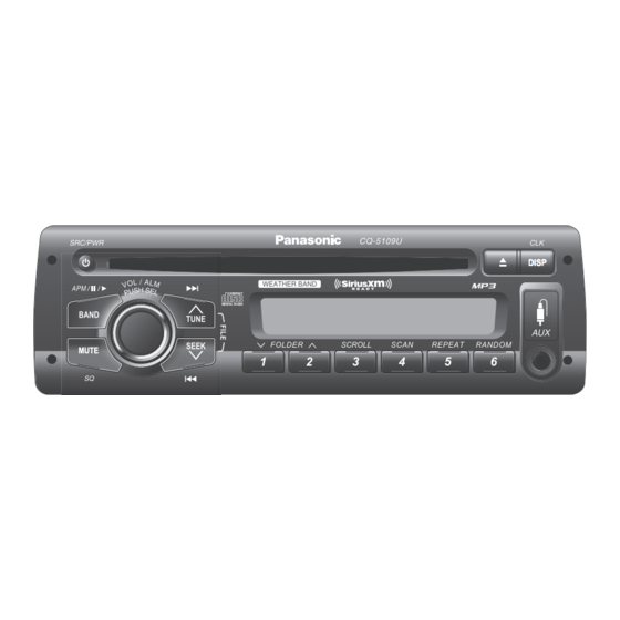
Page 4: Features
3 Features • Front AUX input terminal. • Sound quality control. • SiriusXM Satellite Radio • Alarm function... -
Page 5: Technical Descriptions
4 Technical Descriptions Pin. Port Description FM(V) AM(V) CD(V) 54 E- Electronic Vol-IC clock output. 5.18 5.18 5.19 4.1. Main Block VOL_I2C _SCL IC601:YEAM87835109 55 VDD VDD +5V 5.18 5.18 5.19 56 VSS 57 RADIO_ Radio Tuner EEPROM writing 3.34 3.33 3.36 Pin. - Page 6 Pin No. Port Description Pin No. Port Description D signal input port. 1.81 VPREF 2 Built-in VCO oscillation cooking 0.05 stove setting input terminal. LPF capacitor connection port for 1.76 FE signal. VCOC 2 Built-in VCO control voltage set- 0.05 ting input port.
- Page 7 Pin. PORT Description Segment outputs. 2.58 Segment outputs. 2.58 Segment outputs. 2.58 COM4 Common driver outputs. 2.58 COM3 Common driver outputs. 2.58 COM2 Common driver outputs. 2.58 COM1 Common driver outputs. 2.58 Segment outputs. 2.58 Key scan outputs. 5.17 Key scan outputs. 5.17 Key scan outputs.
- Page 8 4.3. IC Block Diagram 4.3.1. Main Block PAC51:J3CZZZ000003...
- Page 9 IC101:C0CBCYG00004 IC102:C0JBAZ001961...
- Page 10 IC103:C0JBAZ001961 IC104:C0JBAZ001961...
- Page 11 IC301:C1AB00002836...
- Page 12 IC201:C1AA00000788...
- Page 13 IC501:C1BB00001088...
- Page 14 IC51:C0DBEJG00001...
- Page 15 IC701:C0DAZYY00033...
- Page 16 IC702:C0DBEYY00005 IC703:C0EBY0000389...
-
Page 17: Block Diagram
Q900 AUX-IN MODE A/B L/R CH IC501 CTRL2 LCD DI/DO/CD/CLK LOADING MOTOR MOTOR CD+8V D921 KEY MATRIX VR903 DRIVER ILL+9V MODE SW CN902 AUX-IN LCD+5V IC901 LCD COM LCD DISPLAY LCD901 LCD DRIVER LCD SEGMENT SPINDLE MOTOR E-4C413 E-4C425 CQ-5109U... -
Page 18: Schematic Diagram
6 Schematic Diagram 6.1. CD Interface Block... -
Page 19: Wiring Connection Diagram
7 Wiring Connection Diagram 18Pin POWER 4 SPK CONNECTOR BATTERY GROUND Main PCB [E-4C424] <CD Interface Block> Limit SW WIRE Spindle Motor Loading Motor CD Interface PCB Optical Pick-up Assy [E-4C413] Mode SW CQ-5109U... -
Page 20: Schematic Diagram
8 Schematic Diagram 8.1. Main Block... - Page 21 8.2. Display Block...
-
Page 22: Printed Circuit Board
9 Printed Circuit Board 9.1. Main Block (Top View) - Page 23 9.2. Main Block (Bottom View)
- Page 24 9.3. Display Block...
- Page 25 9.4. CD Interface Block...
-
Page 26: Exploded View And Replacement Parts List
10 Exploded View and Replacement Parts List 10.1. Exploded View (Unit) - Page 27 10.2. Replacement Parts List Ref No. Part No. Part Name & DescriptionPart Remarks B0ACCK000005 Diode Notes: B0ECKM000054 Diode 1. Be sure to make your orders of replacement parts accord- B0ECKM000054 Diode B0ECKM000054 Diode ing to this list. D601 B0ACCK000005 Diode 2.
- Page 28 Ref No. Part No. Part Name & DescriptionPart Remarks Ref No. Part No. Part Name & DescriptionPart Remarks C409 F1J1H103A733 Ceramic 0.01μF 50WV C717 F2A1C100A401 Electrolytic 10μF 16WV C410 F1J1H1040014 Ceramic 0.1μF 50WV C718 F2A1C471A035 Electrolytic 470μF 16WV C411 F2A0J101A409 Electrolytic 100μF 6.3WV C719 F2A0J102A031...
- Page 29 Ref No. Part No. Part Name & DescriptionPart Remarks Ref No. Part No. Part Name & DescriptionPart Remarks J161 W6NL Jumper Wire ( 10 mm ) J821 D0YFR00J0001 Chip 0Ω 1/8W J162 W6NL Jumper Wire ( 10 mm ) J823 D0YFR00J0001 Chip 0Ω...
- Page 30 Ref No. Part No. Part Name & DescriptionPart Remarks Ref No. Part No. Part Name & DescriptionPart Remarks R408 D0GD472JA017 Chip 4.7kΩ 1/10W R631 D0GF473JA017 Chip 47kΩ 1/8W R409 D0GD472JA017 Chip 4.7kΩ 1/10W R632 D0GF473JA017 Chip 47kΩ 1/8W R411 D0GD223JA017 Chip 22kΩ...
- Page 31 Ref No. Part No. Part Name & DescriptionPart Remarks Ref No. Part No. Part Name & DescriptionPart Remarks X401 YEXL16M9X54A Crystal SW904 K0H1BA000445 Tack Switch X601 H0A327200171 Crystal SW907 K0H1BA000445 Tack Switch X602 H0A135500004 Crystal SW908 K0H1BA000445 Tack Switch SW909 K0H1BA000445 Tack Switch SURGE PROTECTOR...
- Page 32 Ref No. Part No. Part Name & DescriptionPart Remarks YFS014C110CA Rubber Gum YEXDCM4C174 FX0214C350XA LCD Bracket YFE134C596CA Button (SRC/PWR) YFE134C660ZA Button (TUNE/SEEK/BAND/MUTE) YFE134C597CA Button (EJ/DISP) YFE134C661ZA Button (PRESET) YFC034C265ZA ESC Printing YFE074C092ZA Vol Knob Assy ESC5109U ESC Unit Assy T/RTL YFA054C071CA Under Cover XSB3+6FN...
- Page 33 10.3. Exploded View (CD Deck) YGFD044C017...
- Page 34 10.4. CD Player Parts List Ref No. Part No. Part Name & Description Remarks YDFX02400002 WIRE TUBE MSW Notes: YDFX21800003 ROLLER SHAFT ASSY 1. Be sure to make your orders of replacement parts accord- YDFP05000011 LOADING GEAR PLATE RIVET ASSY YDFP05000012 LOADING PLATE ASSY ing to this list.
- Page 35 10.5. Packing Parts List Item numbers listed below should not order reguler spare parts. (not available) Item No Parts No. Part Name & Description Remarks YFU034C693ZA Inner Carton Not available YFU044C101CB Packing Polylon (Front) Not available YFU044C102CB Packing Polylon (Rear) Not available ZZPR5109U Printing Kit...
-
Page 36: Schematic Diagram For Printing With Letter Size
11 Schematic Diagram for Printing with Letter Size 11.1. Main Block (Left Side) - Page 37 11.2. Main Block (Right Side)
- Page 38 11.3. Display Block (Left Side)
- Page 39 11.4. Display Block (Right Side)
- Page 40 2011.06 (T)
Need help?
Do you have a question about the CQ-5109U and is the answer not in the manual?
Questions and answers