Sony PLM-A55E Service Manual
Personal lcd monitor
Hide thumbs
Also See for PLM-A55E:
- Using instruction (2 pages) ,
- Operating instructions manual (76 pages)
Table of Contents
Advertisement
Quick Links
Advertisement
Table of Contents

Related Manuals for Sony PLM-A55E


Summary of Contents for Sony PLM-A55E
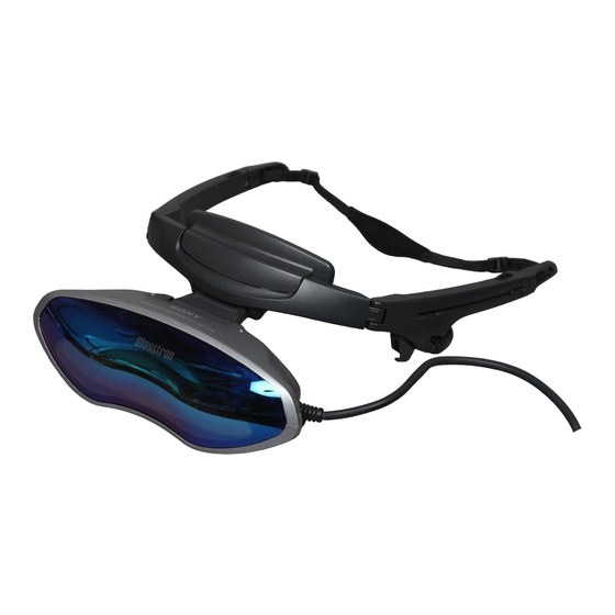
- Page 1 PLM-A55E SERVICE MANUAL AEP Model UK Model SPECIFICATIONS GLASSTRON 9-928-101-31...
-
Page 2: Table Of Contents
LINE WITH MARK ! ON THE SCHEMATIC DIAGRAMS AND IN THE PARTS LIST ARE CRITICAL TO SAFE OPERATION. REPLACE THESE COMPONENTS WITH SONY PARTS WHOSE PART NUMBERS APPEAR AS SHOWN IN THIS MANUAL OR IN SUPPLEMENTS PUB- LISHED BY SONY. - Page 3 SECTION 1 This section is extracted from GENERAL instruction manual. – 3 –...
- Page 4 – 4 –...
- Page 5 – 5 –...
- Page 6 – 6 –...
- Page 7 – 7 –...
- Page 8 – 8 –...
- Page 9 – 9 –...
- Page 10 – 10 –...
- Page 11 – 11 –...
- Page 12 – 12 –...
- Page 13 – 13 –...
- Page 14 – 14 –...
-
Page 15: Disassembly
SECTION 2 DISASSEMBLY Note: Follow the disassembly procedure in the numerical order given. OPTICS OVERALL SECTION 1 screw (M1.4 × 3.0) 2 FP30 flexible board (CN405) 1 three screws (M1.4 × 3.0) 3 optics overall section RG-46 BOARD 5 flexible board (CN402) 2 connector (CN401) - Page 16 2 screw (M1.7) BACK LIGHT UNIT 3 back light unit 1 connector 4 connection (MR) cord OPTICS BLOCK ASS’Y 6 torsion spring 4 boss 1 screw (M1.7 × 4) 2 washer 3 optics black ass’y 4 boss 5 shutter – 16 –...
-
Page 17: Electrical Adjustments
SECTION 3 ELECTRICAL ADJUSTMENTS Precautions on adjustment: 6. Setting up Input Signals 1. Perform the adjustment in the given order. In adjusting this set, video signals obtained from the pattern 2. Power supply voltage: DC 9.0 V generator are used, and therefore these video output signals must 3. -
Page 18: Power Supply Block
[YM-11P board] (Component Side) POWER SUPPLY BLOCK [Power supply voltage check] (YM-11P board) 1. Turn the POWER switch on, and confirm that the POWER LED (green) lights up. 2. Confirm that the voltage at each check land (CL) on the YM- 11P board satisfies the specification value in Table below. - Page 19 [Preparation for Preset Data Writing, Battery Down Adjusting Remote Commander RM-95 (J-6082-053-B) Adjustment, and Charge Threshold Level Adjustment] 1 “Preset Data Writing”, “Battery Down Adjustment”, “Charge NORMAL/SERVICE Threshold Level Adjustment” and all adjustments of “Video mode selection Block” must be performed, if IC901 (EEPROM) on the YM- 11P was replaced.
- Page 20 (3) Operate the adjusting remote commander as follows: • Page change Press the EDIT SEARCH + button to increase the page. Press the EDIT SEARCH – button to decrease the page. There are 16 pages from 0 to F. Hexadecimal numbers 0 1 2 3 4 5 6 7 8 9 A B C D E F LCD display 2 3 4 5 6 7 8 9 A b c d E F...
- Page 21 5. Data Processing Certain adjustment items require the microprocessor data to be read out or the displayed data (hexadecimal numbers) on jigs or adjusting remote commander to be calculated to get adjustment data. In such a case, convert hexadecimal numbers into decimal numbers once, then make calculation, and convert its result into hexadecimal number as adjustment data.
- Page 22 6. Power ON Procedure for Adjustment (1) Connect an extension cable to the adjusting remote commander. (2) After making sure that the HOLD switch on the adjusting remote commander is not turned on (not at left (NOR) position), supply 9.0 Vdc to the DC IN (J301).
- Page 23 [Preset Data Writing] Connection: (1) Connect the adjusting remote commander to the CN902 on YM-11P board. Data Writing Procedure (1) Set data: 01 to page: 1, address: 00. (2) Enter the data given in the table below. Note: To write the data to the EEPROM, press the PAUSE button on the adjusting remote commander each time the data is set. (3) After writing all data, set data: 00 to page: 1, address: 00.
- Page 24 [Battery Down Adjustment] Mode Video/audio signals are output VIDEO IN: Color bar Signal AUDIO IN L: 1kHz, – 20 dBs AUDIO IN R: 1kHz, – 20 dBs Measurement point Displayed data on adj. remote commander Measuring equipment Adjustment page Adjustment address 08, 09, 0A, 0B, 0C, 0D, 42, 43, 44, 45, 46 Specification value ZZh = 5Fh ±...
- Page 25 [Charge Threshold Level Adjustment] Mode Power ON Signal Measurement point Displayed data on adj. remote commander Measuring equipment Adjustment page Adjustment address 0E, 0F, 10, 11, 12 Specification value YYh = D9h ± 09h Connection: Referring to Fig. 3-4, connect the following equipment. (1) Connect the regulated power supply and a digital voltmeter to the battery terminal.
-
Page 26: Video Block
Connection: VIDEO BLOCK Oscilloscope (DC range) To adjust the video block, connect a pattern generator as shown below. As video input signals for adjustment, enter video output signals (color bar signals), unless otherwise specified. (For details, YM-11P Board see page 17) CN102 pin 6 (HAFC) –... -
Page 27: Lcd Block
[RGB Brightness Adjustment] LCD BLOCK Note: The view angle correction must be turned off. Condition: • View angle correction In making the LCD adjustment (except V.COM L adjustment, Chroma signal, and color bar signal with burst Input signal V.COM R adjustment, and white balance adjustment), first short signal turned off the CN404 pin 1 (GND) and pin 2 (EAC OFF) on the RG-46P RG-46P board CN404 pin 4... - Page 28 [Contrast Adjustment] [B Brightness Adjustment] Note: The view angle correction must be turned off. Note: The view angle correction must be turned off. Condition: Before this adjustment, the Contrast Adjustment must be finished. Condition: Chroma signal, and color bar signal with burst Input signal signal turned off Chroma signal, and color bar signal with burst...
- Page 29 [B Gain Adjustment] [R Brightness Adjustment] Note: The view angle correction must be turned off. Note: The view angle correction must be turned off. Before this adjustment, the Contrast Adjustment must be finished. Before this adjustment, the Contrast Adjustment must be finished. Condition: Condition: Chroma signal, and color bar signal with burst...
- Page 30 [R Gain Adjustment] [Burst Cleaning Adjustment] Note: The view angle correction must be turned off. • When Anti-pal signal is available, perform the adjustment shown Before this adjustment, the Contrast Adjustment must be finished. below. Condition: When it isn’t available, fix the data Page: D, address: 36 on A0h. Chroma signal, and color bar signal with burst Note: The view angle correction must be turned off.
- Page 31 [Color Adjustment] [V.COM R] Note: The view angle correction must be turned off. • Make this adjustment through a visual check. Condition: Note: The view angle correction must be turned off. Before this adjustment, the Contrast Adjustment must be finished. Input signal Color bar signal Condition:...
- Page 32 [White Balance Adjustment] • Make this adjustment through a visual check. Note: The view angle correction must be turned off. Condition: Chroma signal, and color bar signal with burst Input signal signal turned off Measurement point LCD screen Measuring equipment Visual check Adjustment page Adjustment address...
- Page 33 Adjustment and Adjustment Parts: [YM-11P Board] (Component Side) Connect adjusting remote commander VIDEO IN jack (J101) CN903 CN902 IC902 IC901 CN301 CN102 2 10 RV101 OSD (On-Screen Display) Horizontal sync frequency adjustment [YM-11P Board] (Conductor Side) IC101 IC103 IC201 IC903 [RG-46P Board] (Component Side) IC401 CN404...
-
Page 34: Diagrams
SECTION 4 DIAGRAMS 4-1. IC PIN FUNCTION DESCRIPTION • RG-46P BOARD IC401 CXA1854AR (LCD VIDEO SIGNAL PROCESSOR, LCD TIMING CONTROL) Pin No. Pin Name Function SYNCIN Video signal (brightness signal) input to the sync separation circuit Video signal (brightness signal) input terminal AGCADJ AGC level setting signal input from the D/A converter (IC402) AGCTC... - Page 35 Pin No. Pin Name Function 3D mode selection signal input from the D/A converter (IC402) “H”: normal mode, “L”: 3D mode TEST7 Input terminal for the test (Normally: open) TEST8 Input terminal for the test (Normally: open) GND2 — Ground terminal (analog system) R OUT R signal (primary color signal) output to the left and right LCD units For DC voltage feedback of R signal (pin #ª)
- Page 36 • YM-11P BOARD IC101 µPD6454GT-628-E2 (CHARACTER GENERATOR) Pin No. Pin Name Function Serial data transfer clock signal input from the system controller (IC903) Chip select signal input from the system controller (IC903) DATA Serial data input from the system controller (IC903) DVDD —...
- Page 37 • YM-11P BOARD IC103 MC141628FUEB (Y/C SEPARATOR A/D, D/A CONVERTER) Pin No. Pin Name Function VCOVDD — Power supply terminal (+5V) (for VCO) BIAS Bias current input terminal (for VCO) VCO control voltage input terminal Signal input from the PCOUT (pin #¡) OSCV DAGND —...
- Page 38 • YM-11P BOARD IC201 CXA1950Q-T4 (RGB DECODER) Pin No. Pin Name Function HUE ADJ HUE adjustment signal input from the D/A converter (IC202) APC (color synchronization) time constant and VXO free-run frequency adjustment signal input APCTC from the D/A converter (IC202) VXO2 —...
- Page 39 • YM-11P BOARD IC903 MB89098RPFV-G-167 (SYSTEM CONTROLLER) Pin No. Pin Name Function TEST MODE 0 Setting terminal for the test mode (Normally: fixed at “L”) TEST MODE 1 Setting terminal for the test mode (Normally: fixed at “L”) Main system clock input terminal (10 MHz) Main system clock output terminal (10 MHz) —...
- Page 40 Pin No. Pin Name Function LED016 to LED021 39 to 44 LED drive signal output terminal Not used (open) RMC SEL Not used (fixed at “L”) RMC SEL — Not used (open) — Power supply terminal (+5V) SEG15 to SEG08 48 to 55 LCD segment drive signal output terminal Not used (open) —...
-
Page 41: Block Diagram - Main Section
4-2. BLOCK DIAGRAM – MAIN Section – PLM-A55E FOR CHECK CN102 (1/2) YM-11P BOARD V IN SC OUT J101 FREERUN ON VIDEO RGB DECODER A/V IN IC201 VIDEO 5.5MHz VIDEO VIDEO CLAMP CLAMP VBSI VBSO BUFFER L.P.F. BUFFER BUFFER VCLPTC... -
Page 42: Block Diagram - Audio/Key Control Section
PLM-A55E 4-3. BLOCK DIAGRAM – AUDIO/KEY CONTROL Section – SA-52P BOARD • Signal path S702 MENU/EXEC : AUDIO MENU D701 POWER DIAL 1 S703 (1/2) PUSH DISPLAY LED DRIVER Q701 SEL/PUSH EXEC (2/2) DIAL 2 D702 CHARGE POWER SW S701... -
Page 43: Block Diagram - Display Section
4-5. BLOCK DIAGRAM – POWER SUPPLY Section – PLM-A55E 4-4. BLOCK DIAGRAM – DISPLAY Section – SA-52P BOARD RG-46P BOARD LCD VIDEO PROCESS, CN701 LCD TIMING CONTROL UNREG LED B+ IC401 CN402 R OUT FILTER SYNC IN G OUT CN401... -
Page 44: Notes For Printed Wiring Board And Schematic Diagram
PLM-A55E 4-7. PRINTED WIRING BOARDS – YM-11P Board/SW-312P Board – (Page 68) (Page 52) • Semiconductor Location 4-6. NOTES FOR PRINTED WIRING BOARD AND SCHEMATIC DIAGRAM (Component Side) Ref. No. Location Ref. No. Location Note on Schematic Diagram: Note on Printed Wiring Board: •... -
Page 45: Schematic Diagram – Ym-11P Board (1/3)
PLM-A55E 4-8. SCHEMATIC DIAGRAM – YM-11P Board (1/3) – • • See pages 80 and 81 for Waveforms. See pages 75 to 78 for IC Block Diagrams. (Page 60) (Page 71) (Page 63) (Page 57) (Page 60) (Page 63) – 53 –... - Page 46 PLM-A55E 4-9. SCHEMATIC DIAGRAM – YM-11P Board (2/3) /SW-312P Board – • See page 81 for Waveforms. • See pages 75 to 78 for IC Block Diagrams. (Page 57) (Page 53) (Page 66) (Page 53) (Page 71) (Page 63) (Page 63)
-
Page 47: Schematic Diagram - Ym-11P Board (1/3)
PLM-A55E 4-10. SCHEMATIC DIAGRAM – YM-11P Board (3/3) – • See pages 81 and 82 for Waveforms. • See pages 75 to 78 for IC Block Diagrams. (Page 57) (Page 57) (Page 57) (Page 56) (Page 57) (Page 53) (Page 57) –... -
Page 48: Schematic Diagram - Sa-52P Board
PLM-A55E 4-11. SCHEMATIC DIAGRAM – SA-52P Board – • See page 75 for IC Block Diagrams. (Page 57) – 64 – – 65 – – 66 –... -
Page 49: Printed Wiring Board - Sa-52P Board
PLM-A55E 4-12. PRINTED WIRING BOARD – SA-52P Board – • Semiconductor • Semiconductor Location Location (Component Side) (Conductor Side) Ref. No. Location Ref. No. Location D501 D507 D502 D701 D505 D702 D509 D703 D510 D704 D511 D708 D705 D706 Q511... -
Page 50: Printed Wiring Board - Rg-46P Board
PLM-A55E 4-13. PRINTED WIRING BOARD – RG-46P Board – (Page 52) (Page 52) • Semiconductor Location (Component Side) Ref. No. Location D405 D407 IC401 Q403 Q404 Q410 Q411 • Semiconductor Location (Conductor Side) Ref. No. Location D406 IC402 Q401 Q402... -
Page 51: Schematic Diagram - Rg-46P Board
PLM-A55E 4-14. SCHEMATIC DIAGRAM – RG-46P Board – • See page 82 for waveforms. • See pages 77 to 79 for IC Block Diagrams. (Page 56) (Page 57) – 71 – – 72 – – 73 – – 74 –... - Page 52 PLM-A55 • IC Block Diagrams IC202 MB88346BPFV-EF (YM-11P Board) IC504 BA3574BFS-E2 (SA-52P Board) IC501 M5222FP-E1 (SA-52P Board) IC103 MC141628FUEB (YM-11P Board) IC402 MB88346BPFV-EF (RG-46P Board) IC301 MB3785APFV-G-BND-ER (YM-11P Board) MUTE SW 11 MUTE MUTE OUT1 36 35 34 33 32 31 30 28 27 26 25...
- Page 53 IC401 CXA1854AR-T6 (RG-46P Board) GND 2 +12V REG. REGV TEST 5 V. SYNC SEP S-Y IN CLAMP INT/EXT R-Y IN V. POS PAL ID RESET GEN C OUT DEMOD PAL SW V. CTL V. POS POL SW COUNTER COUNTER HCK 1 HUE/RST RESET XCLR...
- Page 54 • Waveforms – YM-11P Board (1/3) – 1 IC101 @¢ (AFDO) 6 IC103 !• (V IN) !¡ Q254 Emitter 4.9 Vp-p 440 mVp-p 0.7 Vp-p 2 IC101 !ª (VBSI) 7 IC103 @ª (CLK IN) !™ Q264 Emitter 536 mVp-p 1.0 Vp-p 0.5 Vp-p 279 ns 3 IC101 !¶...
- Page 55 !§ IC201 5 (SC OUT) 2 IC903 `⁄‚‚ (CL0) 4 IC301 $¶ (NF A) 2.5 Vp-p 560 mVp-p 1.6 Vp-p 32 KHz 4.433619 MHz 3.27 µ s !¶ IC201 8 (B/B-Y) 5 IC301 $¡ (NF C) 1.6 Vp-p 2.5 Vp-p –...
- Page 56 9 Q301 1 (Base) 3 Q406 Base 8 IC401 $¡ (G OUT) 960 mVp-p 424 mVp-p 9.6 Vp-p 3.27 µ s 0 Q312 1 (Base) 4 IC401 2 (YIN) 9 IC401 $£ (B OUT) 300 mVp-p 9.6 Vp-p 1.2 Vp-p 3.27 µ...
-
Page 57: Exploded Views
SECTION 5 EXPLODED VIEWS NOTE: The components identified by • -XX and -X mean standardized parts, so they • Items marked “*” are not stocked since they mark ! or dotted line with mark are seldom required for routine service. Some may have some difference from the original ! are critical for safety. - Page 58 (2) DISPLAY UNIT SECTION-2 (LOADING BLOCK ASS’Y) not supplied not supplied not supplied HP402 not supplied not supplied not supplied not supplied not supplied HP401 not supplied Ref. No. Part No. Description Remark Ref. No. Part No. Description Remark 3-704-197-32 SCREW (M1.4X3.0) X-3948-504-2 CABINET (R) ASSY 3-050-017-02 COVER (REAR), HINGE 3-988-782-01 BUTTON (R), RELEASE...
- Page 59 (3) POWER SUPPLY BOX SECTION Ref. No. Part No. Description Remark Ref. No. Part No. Description Remark * 108 3-988-800-01 RETAINER, TERMINAL X-3948-508-2 CABINET (IF) ASSY, UPPER 3-988-786-01 BUTTON, BATTERY RELEASE A-8054-836-A SW-312P BOARD, COMPLETE A-8054-833-A YM-11P BOARD, COMPLETE 3-050-073-01 KNOB, POWER A-8054-835-A SA-52P BOARD, COMPLETE 1-783-687-12 CORD, CONNECTION (MR) 3-945-884-11 SCREW (2X6)
-
Page 60: Electrical Parts List
SECTION 6 RG-46P ELECTRICAL PARTS LIST NOTE: • Due to standardization, replacements in the • Items marked “*” are not stocked since they The components identified by mark ! or dotted line with mark parts list may be different from the parts speci- are seldom required for routine service. - Page 61 RG-46P Ref. No. Part No. Description Remark Ref. No. Part No. Description Remark D422 8-719-017-13 DIODE 02DZ7.5 -TPH3 R419 1-216-815-91 RES, CHIP 1/16W R421 1-216-819-91 RES, CHIP 1/16W < SHORT > R422 1-216-833-91 RES, CHIP 1/16W FB401 1-543-962-22 FERRITE R423 1-216-833-91 RES, CHIP 1/16W FB402...
- Page 62 RG-46P SA-52P Ref. No. Part No. Description Remark Ref. No. Part No. Description Remark R482 1-216-821-91 RES, CHIP 1/16W C525 1-124-778-21 ELECT CHIP 22uF 6.3V R483 1-216-821-91 RES, CHIP 1/16W C526 1-164-346-91 CERAMIC CHIP R484 1-216-821-91 RES, CHIP 1/16W C527 1-124-779-21 ELECT CHIP 10uF R485...
- Page 63 SA-52P SW-312P YM-11P Ref. No. Part No. Description Remark Ref. No. Part No. Description Remark < TRANSISTOR > R702 1-216-864-91 SHORT R703 1-216-817-91 RES, CHIP 1/16W Q501 8-729-402-85 TRANSISTOR XN4601-TW Q502 8-729-402-85 TRANSISTOR XN4601-TW R704 1-216-817-91 RES, CHIP 1/16W Q503 8-729-029-14 TRANSISTOR DTC144EUA-T106 Q508 8-729-420-26 TRANSISTOR 2SB1218A-QRS-TX...
- Page 64 YM-11P Ref. No. Part No. Description Remark Ref. No. Part No. Description Remark C160 1-135-259-91 TANTAL. CHIP 10uF 6.3V C253 1-135-259-91 TANTAL. CHIP 10uF 6.3V C161 1-135-259-91 TANTAL. CHIP 10uF 6.3V C255 1-162-974-91 CERAMIC CHIP 0.01uF C162 1-164-346-91 CERAMIC CHIP C257 1-135-259-91 TANTAL.
- Page 65 YM-11P Ref. No. Part No. Description Remark Ref. No. Part No. Description Remark C901 1-135-259-91 TANTAL. CHIP 10uF 6.3V CN902 1-691-550-21 PIN, CONNECTOR (1.5mm) (SMD) 3P C902 1-162-974-91 CERAMIC CHIP 0.01uF * CN903 1-695-320-21 PIN, CONNECTOR (1.5mm) (SMD) 2P C903 1-164-156-91 CERAMIC CHIP 0.1uF <...
- Page 66 YM-11P Ref. No. Part No. Description Remark Ref. No. Part No. Description Remark FB603 1-543-949-22 FERRITE < IC LINK > FB901 1-216-295-91 SHORT FB902 1-216-295-91 SHORT PS901 1-576-123-21 LINK, IC FB903 1-216-295-91 SHORT FB904 1-216-295-91 SHORT < TRANSISTOR > < FILTER > Q101 8-729-420-29 TRANSISTOR 2SD1819A-QRS-TX Q102...
- Page 67 YM-11P Ref. No. Part No. Description Remark Ref. No. Part No. Description Remark Q601 8-729-420-29 TRANSISTOR 2SD1819A-QRS-TX R158 1-216-805-91 RES, CHIP 1/16W R159 1-216-823-91 RES, CHIP 1.5K 1/16W Q602 8-729-420-29 TRANSISTOR 2SD1819A-QRS-TX R160 1-216-864-91 SHORT Q901 8-729-029-14 TRANSISTOR DTC144EUA-T106 R162 1-216-864-91 SHORT Q902 8-729-420-13 TRANSISTOR XN4213-TW...
- Page 68 YM-11P Ref. No. Part No. Description Remark Ref. No. Part No. Description Remark R229 1-216-821-91 RES, CHIP 1/16W R297 1-216-833-91 RES, CHIP 1/16W R298 1-216-833-91 RES, CHIP 1/16W R230 1-216-827-91 RES, CHIP 3.3K 1/16W R299 1-543-949-22 FERRITE R231 1-216-839-91 RES, CHIP 1/16W R301 1-218-887-91 RES, CHIP...
- Page 69 YM-11P Ref. No. Part No. Description Remark Ref. No. Part No. Description Remark R364 1-218-878-91 RES, CHIP 0.50% 1/16W R927 1-216-833-91 RES, CHIP 1/16W R365 1-218-865-91 RES, CHIP 5.6K 0.50% 1/16W R928 1-216-817-91 RES, CHIP 1/16W R366 1-218-895-91 RES, CHIP 100K 0.50% 1/16W R929...
- Page 70 PLM-A55E Ref. No. Part No. Description Remark Ref. No. Part No. Description Remark < SWITCH > S901 1-571-787-11 SWITCH, TACTILE (PASSWORD RESET) < TRANSFORMER > T301 1-429-719-21 TRANSFORMER, DC-DC CONVERTER < VIBRATOR > X101 1-579-780-61 VIBRATOR, CRYSTAL (17.734475MHz) X201 1-579-661-41 OSCILLATOR, CRYSTAL (4.433619MHz) X901 1-767-300-21 VIBRATOR, CRYSTAL (32.768kHz)
Need help?
Do you have a question about the PLM-A55E and is the answer not in the manual?
Questions and answers