Table of Contents
Advertisement
QQ
3 7 63 1515 0
SERVICE MANUAL
01
2003
49768
TE
L 13942296513
1
Important Safety Precautions . . . . . . . . . . . . . . . . . . . . . . . . . . . . . . . . . . . . . . . . . . . . . . . . . . . . . . . . . . . 1-2
2
Disassembly method . . . . . . . . . . . . . . . . . . . . . . . . . . . . . . . . . . . . . . . . . . . . . . . . . . . . . . . . . . . . . . . . . . 1-4
3
Adjustment. . . . . . . . . . . . . . . . . . . . . . . . . . . . . . . . . . . . . . . . . . . . . . . . . . . . . . . . . . . . . . . . . . . . . . . . . . 1-23
4
Description of major ICs . . . . . . . . . . . . . . . . . . . . . . . . . . . . . . . . . . . . . . . . . . . . . . . . . . . . . . . . . . . . . . . 1-27
www
.
http://www.xiaoyu163.com
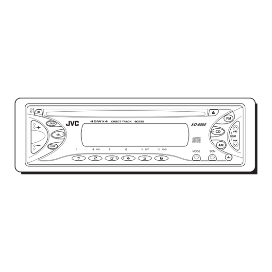
CD RECEIVER
KD-S595
LOUD
SEL
TABLE OF CONTENTS
x
ao
u163
y
i
COPYRIGHT © 2003 VICTOR COMPANY OF JAPAN, LTD.
http://www.xiaoyu163.com
2 9
8
DIRECT TRACK
CCESS
A
Q Q
3
6 7
1 3
1 5
co
.
9 4
2 8
0 5
8
2 9
9 4
2 8
Area Suffix
U ----------------- Other Areas
m
No.49768
KD-S595
9 9
9 9
2003/01
Advertisement
Chapters
Table of Contents

Related Manuals for JVC KD-S595


Summary of Contents for JVC KD-S595
- Page 1 KD-S595 3 7 63 1515 0 SERVICE MANUAL CD RECEIVER 49768 2003 KD-S595 DIRECT TRACK CCESS LOUD L 13942296513 Area Suffix U ----------------- Other Areas TABLE OF CONTENTS Important Safety Precautions ............1-2 Disassembly method .
-
Page 2: Important Safety Precautions
KD-S595 3 7 63 1515 0 SECTION 1 Important Safety Precautions 1.1 Safety Precautions Burrs formed during molding may be left over on some parts of the chassis. Therefore, pay attention to such burrs in the case of preforming repair of this system. - Page 3 KD-S595 3 7 63 1515 0 1.2 Preventing static electricity Electrostatic discharge (ESD), which occurs when static electricity stored in the body, fabric, etc. is discharged, can destroy the laser diode in the traverse unit (optical pickup). Take care to prevent this when performing repairs.
-
Page 4: Disassembly Method
KD-S595 3 7 63 1515 0 SECTION 2 Disassembly method 2.1 Main body 2.1.1 Removing the front panel assembly Front panel assembly (See Fig.1) (1) Push the detach button in the lower right part of the front panel assembly and remove the front panel assembly in the direction of the arrow. -
Page 5: Http://Www.xiaoyu163.Com
KD-S595 3 7 63 1515 0 2.1.3 Removing the heat sink (See Fig.4) (1) Remove the two screws B and two screws C on the left side of the main body. Heat sink Fig.4 2.1.4 Removing the bottom cover (See Figs.5 and 6) - Page 6 KD-S595 3 7 63 1515 0 2.1.6 Removing the main board Main board assembly (See Fig.8) • Prior to performing the following procedure, remove the front panel assembly, front chassis assembly, heat sink, bottom cover and rear bracket (1) Remove the two screws G attaching the main board.
- Page 7 KD-S595 3 7 63 1515 0 2.1.8 Removing the front board (See Figs.10 to 12) • Prior to performing the following procedure, remove the front panel assembly. (1) Remove the four screws J on the back side of the front pan- el assembly.
- Page 8 KD-S595 3 7 63 1515 0 2.2 CD Mechanism Assembly 2.2.1 Removing the top cover (See Figs.1 and 2) (1) Remove the two screws A on the both side of the body. (2) Lift the front side of the top cover and move the top cover backward to release the two joints a.
- Page 9 KD-S595 3 7 63 1515 0 2.2.2 Removing the connector board Wires (See Figs.3 to 5) CAUTION: Before disconnecting the flexible wire from the pickup, solder the short-circuit point on the pickup. No observance of this in- struction may cause damage of the pickup.
- Page 10 KD-S595 3 7 63 1515 0 2.2.3 Removing the DET switch (See Figs.6 and 7) (1) Extend the two tabs c of the feed sw. holder and pull out the switch. (2) Unsolder the DET switch wire if necessary.
- Page 11 KD-S595 3 7 63 1515 0 2.2.4 Removing the chassis unit (See Figs.8 and 9) • Prior to performing the following procedure, remove the top Chassis unit cover and connector board. Suspension spring (L) Suspension spring (R) (1) Remove the two suspension springs (L) and (R) attaching the chassis unit to the frame.
- Page 12 KD-S595 3 7 63 1515 0 2.2.5 Removing the clamper assembly (See Figs.10 and 11) • Prior to performing the following procedure, remove the top cover. (1) Remove the clamper arm spring. Clamper arm spring (2) Move the clamper assembly in the direction of the arrow to release the two joints d.
- Page 13 KD-S595 3 7 63 1515 0 2.2.6 Removing the loading / feed motor assembly (See Figs.12 and 13) • Prior to performing the following procedure, remove the top cover, connector board and chassis unit. (1) Remove the screw C and move the loading / feed motor as- sembly in the direction of the arrow to remove it from the chassis rivet assembly.
- Page 14 KD-S595 3 7 63 1515 0 2.2.7 Removing the pickup unit Pickup unit (See Figs.14 to 18) • Prior to performing the following procedure, remove the top cover, connector board and chassis unit. (1) Remove the screw D and pull out the pu. shaft holder from Part e the pu.
- Page 15 KD-S595 3 7 63 1515 0 2.2.9 Removing the trigger arm Joint k (See Figs.19 and 20) • Prior to performing the following procedure, remove the top cover, connector board and clamper unit. (1) Turn the trigger arm in the direction of the arrow to release Trigger arm the joint k and pull out upward.
- Page 16 KD-S595 3 7 63 1515 0 2.2.11 Removing the mode sw. / select lock arm Link plate Joint t (See Figs.22 and 23) Mode sw. • Prior to performing the following procedure, remove the top plate assembly. Select lock arm (1) Bring up the mode sw.
- Page 17 KD-S595 3 7 63 1515 0 2.2.12 Reassembling the mode sw. / select lock arm Select lock arm spring (See Figs.24 to 26) Hook w REFERENCE: Reverse the above removing procedure. Joint v (1) Reattach the select lock arm spring to the top plate and set...
- Page 18 KD-S595 3 7 63 1515 0 2.2.13 Removing the select arm R / link plate Joint c' Link plate Joint r (See Figs.27 and 28) Select arm R Joint b' • Prior to performing the following procedure, remove the top plate assembly.
- Page 19 KD-S595 3 7 63 1515 0 2.2.15 Removing the loading roller assembly Loading roller assembly (See Figs.31 to 33) • Prior to performing the following procedure, remove the Roller guide spring clamper assembly and top plate assembly. (1) Push inward the loading roller assembly on the gear side and detach it upward from the slot of the joint g' of the lock arm rivet assembly.
- Page 20 KD-S595 3 7 63 1515 0 2.2.16 Removing the loading gear 5, 6 and 7 Loading gear bracket (See Figs.35 and 36) • Prior to performing the following procedure, remove the top Loading gear 6 cover, chassis unit, pickup unit and top plate assembly.
-
Page 21: Pull Out The Loading Gear
KD-S595 3 7 63 1515 0 2.2.17 Removing the gears Joint p' (See Figs.37 to 40) • Prior to performing the following procedure, remove the top Change plate rivet assembly cover, chassis unit, top plate assembly and pickup unit. -
Page 22: Http://Www.xiaoyu163.Com
KD-S595 3 7 63 1515 0 2.2.18 Removing the turn table / spindle motor Turn table (See Figs.41 and 42) • Prior to performing the following procedure, remove the top cover, connector board, chassis unit and clamper assembly. (1) Remove the two screws L attaching the spindle motor as- sembly through the slot of the turn table on top of the body. -
Page 23: Adjustment
6. Digital tester FM 87.5MHz ~ 107.9MHz 7. Tracking offset meter AM 531kHz ~ 1602 kHz 8. Test Disc JVC : CTS-1000 9. Extension cable for check EXTSH002-22P × 1 Dummy load Exclusive dummy load should be used for AM, and FM. For FM dummy load, there is a loss of 6dB between SSG output and antenna input. - Page 24 KD-S595 3 7 63 1515 0 3.2 Troubleshooting 3.2.1 Feed section Is the voltage output at Is the wiring for IC541 Is 5V present at IC581 Check CD 9V IC541 pin 4 is 5V or 0V? 1 ~ 14 correct? pin 6? and 5V.
- Page 25 KD-S595 3 7 63 1515 0 3.2.5 Signal processing section No sound from either Compare the L-ch and R-ch Is the sound output from channel. to locate the defective point. both channels (L, R)? Check the vicinity of the...
- Page 26 KD-S595 3 7 63 1515 0 3.3 Maintenance of laser pickup 3.4 Replacement of laser pickup (1) Cleaning the pick up lens Before you replace the pick up, please try to clean the lens Turn off the power switch and,disconnect the power cord with a alcohol soaked cotton swab.
-
Page 27: Description Of Major Ics
KD-S595 3 7 63 1515 0 SECTION 4 Description of major ICs 4.1 HA13164A (IC901) : Regulator • Pin layout 1 2 3 4 5 6 7 8 9 10 11 12 13 14 15 • Block diagram 100u 0.1u... - Page 28 KD-S595 3 7 63 1515 0 4.2 AN8806SB-W (IC501) : RF & amp. • Pin layout 36 PDAC PD 1 LD 2 35 PDBD 34 PDF LDON 3 LDP 4 33 PDE 32 PDER VCC 5 RF- 6 31 PDFR...
- Page 29 KD-S595 3 7 63 1515 0 • Pin function Pin No. Symbol Function APC amp input terminal APC amp output terminal LD ON APC ON/OFF control terminal Connect to ground Power supply Inverse input pin for RF amp RF OUT...
- Page 30 KD-S595 3 7 63 1515 0 4.3 TEA6320T-X (IC301) : E.volume • Pin layout OUTRR OUTLR OUTRF OUTLF Vref MUTE CD-CH TAPE TUNER • Block diagram VOLUME 2 MUTE 0 to 55 dB FUNCTION BALANCE ZERO CROSS FENDER REAR...
- Page 31 KD-S595 3 7 63 1515 0 4.4 NJM4565M-WE (IC151) : CD L.P.F. • Pin layout & Block diagram A OUTPUT B OUTPUT A INPUT B INPUT A INPUT B INPUT L 13942296513 u163 (No.49768)1-31 http://www.xiaoyu163.com...
- Page 32 KD-S595 3 7 63 1515 0 4.5 JES01-9B42 (IC801) : Main micon • Pin layout • Pin function Pin No. Symbol Function X'tal oscillator conection terminal TEST2 J BUS SI Non connect J BUS SO Non connect J BUS SCK...
- Page 33 KD-S595 3 7 63 1515 0 Pin No. Symbol Function RELAY Power supply control terminal BLKCL Sub code/ Block signal input terminal BEEP Non connect Detection switch 1 Detection switch 2 Pnael switch detection REST Rest switch input terminal...
-
Page 34: Table Of Contents
KD-S595 3 7 63 1515 0 4.6 LA4743K (IC321) : Power amp. • Block diagram 2200 F 0.022 F Vcc 1/2 Vcc 3/4 IN 1 OUT 1+ 0.22 F OUT 1- PWR GND1 Protective circuit OUT 2+ IN 2 OUT 2- 0.22 F... -
Page 35: Tab
KD-S595 3 7 63 1515 0 • Pin layout • Pin function Pin No. Symbol Function Header of IC Power GND Outpur(-) for front Rch STDBY Stand by input Output (+) for front Rch Power input Output (-) for rear Rch... -
Page 36: Mute
KD-S595 3 7 63 1515 0 4.7 LA6589H-X (IC541) : BTL driver • Pin layout & Block diagram VIN1-A VIN1 VIN1_SW H : OP-AMP_A L : OP-AMP_B VIN1+A VIN1-B VCCP1 VIN1+B VO1+ S-GND Signal system VO1- VIN1-SW It is ON/OFF as for all outputs. -
Page 37: Ao Y U163
KD-S595 3 7 63 1515 0 • Pin function Pin No. Symbol Function VIN1-A CH1 input AMP_A reversing input VIN1+A CH1 input AMP_A non-reversing input VCCP1 CH1 and CH2 power steps power supply VO1+ CH1 Output terminal (+) VO1-... -
Page 38: Out
KD-S595 3 7 63 1515 0 4.8 MN6627482WA (IC561) : DSP & DAC • Pin layout 20 ~ 41 ~ • Block diagram AVSS1 LRCKIN(MSEL) 8TIMES AVDD1 BCLK(SSEL) DIGITAL OVER SAMPUNC OUTR SRDATAIN DEEMPHSIS 1BIT DIGITAL FILTER (PSEL) LOGIC... -
Page 39: Out
KD-S595 3 7 63 1515 0 • Pin function Pin No. Symbol Function Pin No. Symbol Function WVEL Not used BCLK Not used RF signal input LRCK Not used IREF Reference current input pin SRDATA Not used Bias pin for DSL... - Page 40 KD-S595 3 7 63 1515 0 4.9 PT6523LQ (IC601) : LCD driver • Pin layout • Block diagram COMMON SEGMENT DRIVER & LATCH DRIVER CLOCK GENERATOR SHIFT REGISTER ADDRESS DETECTOR L 13942296513 • Piin function Pin No. Pin Name...
- Page 41 KD-S595 3 7 63 1515 0 L 13942296513 u163 (No.49768)1-41 http://www.xiaoyu163.com...
- Page 42 KD-S595 3 7 63 1515 0 L 13942296513 u163 VICTOR COMPANY OF JAPAN, LIMITED AV & MULTIMEDIA COMPANY 10-1,1chome,Ohwatari-machi,Maebashi-city,371-8543,Japan (No.49768) Printed in Japan 200301WPC http://www.xiaoyu163.com...
-
Page 43: Schematic Diagrams
KD-S595 3 7 63 1515 0 SCHEMATIC DIAGRAMS CD RECEIVER KD-S595 CD-ROM No.SML200301 DIR E C T T R A C K A C C E S S LOUD L 13942296513 Area suffix U --------------------- Other Areas Contents Block diagram... -
Page 44: Safety Precaution
KD-S595 3 7 63 1515 0 Safety precaution Burrs formed during molding may be left over on some parts of the chassis. Therefore, pay attention to such burrs in the case of preforming repair of this system. Please use enough caution not to see the beam directly or touch it in case of an adjustment or operation check. - Page 45 KD-S595 3 7 6 3 1 5 1 5 0 Block diagram CJ701 TU701 CJ321 TU.LCH FM/AM LINE OUT TU.RCH TUNER SW1,SW2,PSW FM/AM MONO LM,MSW TRV,TVD, FM.OSC ECM,ECS, IC321 SPINDLE+ IC301 CD.SENSE KICK,TRD,FOD IC561 IC541 OUT LF POWER SPINDLE- E.VOL...
- Page 46 KD-S595 KD-S595 3 7 6 3 1 5 1 5 0 Standard schematic diagrams Main amplifier section TU701 QAU0281-001 CJ701 QNB0100-002 Q861 L701 4.7u UN2111-X MUTE R201 R703 R101 R701 R333 R334 CJ321 D332 R336 2.2k Q332 2SD1781K/QR/-X 1SS355-X...
- Page 47 KD-S595 3 7 6 3 1 5 1 5 0 CD servo control section D551 1A3G-T1 C552 C551 0.01 220/10 C543 0.033 R596 8.2k C541 IC561 22/16 MN6627482WA Q541 2SA1706/ST/-T C540 CD8V CD.RESET STATUS KICK IC541 SUBQ C570 SQCK LA6589H-X 0.022...
- Page 48 KD-S595 KD-S595 3 7 6 3 1 5 1 5 0 LCD & Key control section IC602 RPM6938-SV4 C611 0.012 C612 R662 4.7/6.3 D644 UDZS6.2B-X CJ601 VMC0355-001 R661 LCD1 ILL-10V QLD0210-002 REMOCON Main amplifier section CN801 LCD.CLK LCD.SO IC601 LCD.CE...
- Page 49 KD-S595 3 7 63 1515 0 Printed circuit boards Main board Reverse side D904 R862 C915 C901 R861 L901 R911 D869 IC901 D867 D861 C996 R904 C902 Q332 C862 D901 C910 C905 R903 R336 R902 C331 C906 D903 C303...
- Page 50 KD-S595 3 7 63 1515 0 Front board Forward side D620 S619 D615 R616 R611 S604 R610 D603 D601 R617 S620 S603 R604 D616 D604 R638 R602 D731 R639 R615 R601 R614 S602 S607 R606 S605 D732 R637 S617...
- Page 51 KD-S595 3 7 63 1515 0 < M E M O > L 13942296513 u163 http://www.xiaoyu163.com...
- Page 52 KD-S595 3 7 63 1515 0 L 13942296513 u163 VICTOR COMP ANY OF JAP AN, LIMITED AV & MULTIMEDIA COMPANY 10-1,1Chome,Ohwatari-machi,Maebashi-city,371-8543,Japan Printed in Japan (No.49768SCH) 2003/01 http://www.xiaoyu163.com...
-
Page 53: Parts List
KD-S595 3 7 63 1515 0 PARTS LIST [ KD-S595 ] * All printed circuit boards and its assemblies are not available as service parts. Area suffix U ---------------------- Other Areas L 13942296513 - Contents - 3- 2 Exploded view of general assembly and parts list (Block No.M1) 3- 4 CD mechanism assembly and parts list (Block No.MB) - Page 54 KD-S595 3 7 63 1515 0 L 13942296513 u163 http://www.xiaoyu163.com...
- Page 55 KD-S595 3 7 63 1515 0 Parts list (General assembly) Block No. M1MM Item Parts number Parts name Q'ty Description Area --------------------- CD MECHA GE10043-205A TOP CHASSIS GE40135-001A EARTH PLATE GE30568-006A HEAT SINK GE30393-002A BOTTOM COVER FSMA3004-203 INSULATOR SCREW...
- Page 56 KD-S595 3 7 63 1515 0 CD mechanism assembly and parts list Block No. Grease TNG-87 TN-2001-1011 GP-501MK CFD-005Z GP-501A L 13942296513 u163 http://www.xiaoyu163.com...
-
Page 57: Loading Gear
KD-S595 3 7 63 1515 0 Parts list (CD mechanism) Block No. MBMM Item Description Parts number Parts name Q'ty Area 30320101T FRAME 30320102T TOP COVER 30320115T DANPER F 30320116T DANPER R 303205505T CHASSIS RIVET 303205503T CHANGE P. RVT A... -
Page 58: Loading Gear
KD-S595 Parts list (CD mechanism) Block No. MBMM 3 7 63 1515 0 Item Parts number Parts name Q'ty Description Area 30321103T LOADING GEAR 3 30321104T LOADING GEAR 4 30321105T LOADING GEAR 5 30321106T LOADING GEAR 6 30321107T LOADING GEAR 7... - Page 59 KD-S595 3 7 63 1515 0 Electrical parts list (Main board) Block No. 01 Item Parts number Parts name Remarks Area Item Remarks Parts number Parts name Area C 101 QERF1HM-105Z E CAPACITOR 1.0MF 20% 50V C 520 NDC31HJ-470X...
- Page 60 KD-S595 3 7 63 1515 0 Electrical parts list (Main board) Block No. 01 Item Parts number Parts name Remarks Area Item Parts number Parts name Remarks Area C 906 NCB31EK-104X C CAPACITOR Q 793 UN2211-X TRANSISTOR C 907...
- Page 61 KD-S595 3 7 63 1515 0 Electrical parts list (Main board) Block No. 01 Item Parts number Parts name Remarks Area Item Parts number Parts name Remarks Area R 547 NRSA63J-224X MG RESISTOR R 829 NRS181J-473X MG RESISTOR R 548...
- Page 62 KD-S595 3 7 63 1515 0 Electrical parts list (Front board) Block No. 02 Item Parts number Parts name Remarks Area Item Parts number Parts name Remarks Area C 601 NCB31HK-223X C CAPACITOR R 655 NRSA63J-103X MG RESISTOR C 602...
- Page 63 KD-S595 3 7 63 1515 0 < M E M O > L 13942296513 u163 3-11 http://www.xiaoyu163.com...
- Page 64 KD-S595 3 7 63 1515 0 Packing materials and accessories parts list Block No. Block No. A1~A4 L 13942296513 KIT : A5~A9 u163 3-12 http://www.xiaoyu163.com...
- Page 65 KD-S595 3 7 63 1515 0 Parts list (Packing) Block No. M3MM Item Description Parts number Parts name Q'ty Area POLY BAG 1 INST.BOOK FSPG4002-001 QPA00801205 POLY BAG QPA01003003 POLY BAG 1 FOR HARD CASE FSYH4036-068 SHEET QPC03004315P POLY BAG 1 SET(260X440X0.0...
Need help?
Do you have a question about the KD-S595 and is the answer not in the manual?
Questions and answers