Sony BDP-S485 Service Manual
Dvd
Hide thumbs
Also See for BDP-S485:
- Operating instructions manual (35 pages) ,
- Troubleshooting manual (10 pages)
Table of Contents
Advertisement
SERVICE MANUAL
Ver. 1.2 2012. 04
System
Laser: Semiconductor laser
Inputs and Outputs:
(Jack name:Jack type/Output level/Load impedance)
Line Out R-Audio-L:
Phone jack/2 Vrms/10 kilohms
Digital Out(Coxial):
Phono jack/0.5 Vp-p/75 ohms
HDMI Out :
HDMI 19-pin standard connector
Component Video out:
(Y, P
, P
) :
B
R
Phono jack/Y: 1.0 Vp-p/
P
, P
: 0.7 Vp-p/75 ohms
B
R
Line Out Video:
Phono jack/1.0 Vp-p/75 ohms
LAN (100):
100BASE-TX Terminal
USB:
USB jack Type A (For connecting a USB memory,
memory card reader,digital still camera and digital
video camera)
9-890-747-13
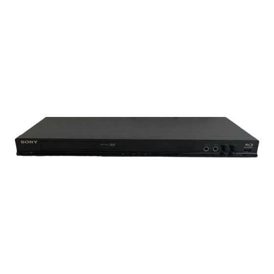
Photo: BDP-S485
Remote : RMT-B111P
SPECIFICATIONS
Sony Corporation
Home Entertainment Business Group
BDP-S485
China Model
Singapore Model
Russian Model
Thailand Model
General
Power requirements:
220 – 240V AC, 50/60Hz (RUS,CN)
110 – 240V AC, 50/60Hz (SP,TH)
Power consumption:
20W (BDP-S485)
Dimensions (approx.):
430 mm × 199 mm × 36mm
(17 in. × 7
4
/
in. × 1
7
/
in.)
5
16
(width/depth/height) incl. projecting parts
Mass (approx.):
1
7 . .
g k
Operating temperature:
º
º
5 ºC to 35 ºC(41 F to 95 F)
Operating humidity:
25 % to 80 %
Supplied accessories:
• Audio/video cable (phono plug ×3) (1)
(
BDP-S495:RUS ONLY)
LAN cable
•
(1) (BDP-S480 :
only)
TW
• HDMI cable (1) (BDP-S458:SP,TH,CN)
• Remote commander (remote) (1)
• Size AA (R6) batteries (2)
Specifications and design are subject to change
without notice.
TM
BLU-RAY DISC / DVD PLAYER
Published by Design Engineering Dept.
RMT-B111C/B111P
2012D6900-1
© 2012.04
Advertisement
Chapters
Table of Contents

Related Manuals for Sony BDP-S485


Summary of Contents for Sony BDP-S485
-
Page 1: Specifications
BDP-S485 RMT-B111C/B111P SERVICE MANUAL China Model Singapore Model Russian Model Ver. 1.2 2012. 04 Thailand Model Photo: BDP-S485 Remote : RMT-B111P SPECIFICATIONS System General Power requirements: Laser: Semiconductor laser Inputs and Outputs: 220 – 240V AC, 50/60Hz (RUS,CN) (Jack name:Jack type/Output level/Load impedance) 110 –... - Page 2 CRITIQUES POUR LA SÉCURITÉ DE FONCTIONNEMENT. NE ordinary solder so use caution not to let solder bridges occur such REMPLACER CES COMPOSANTS QUE PAR DES PIÈSES SONY as on IC pins, etc. DONT LES NUMÉROS SONT DONNÉS DANS CE MANUEL OU •...
-
Page 3: Table Of Contents
BDP-S485 TABLE OF CONTENTS SERVICE NOTE 1-1. Disc Removal Procedure If The Tray Cannot Be 4-12. MB-139 Board (HDMI) Ejected (Forced Ejection) ..........1-1 Schematic Diagram (7/17)..........4-12 1-2. Work when optical device are replaced ......1-1 4-13. MB-139 Board (ETHERNET) 1-3. -
Page 4: Service Note
BDP-S485 SECTION 1 SERVICE NOTE 1-1. DISC REMOVAL PROCEDURE IF THE TRAY CANNOT BE EJECTED (FORCED EJECTION) 1. Remove the upper case. (Refer to page 2-1) 2. Insert a clip in the hole of a drive and open a tray. -
Page 5: Test Disc
BDP- S485 1-3. TEST DISC Part No. Description Layer J-6090-199-A BLX-104 Single Layer J-6090-200-A BLX-204 Dual Layer J-2501-307-A CD (HLX-A1) J-2501-305-A HLX-513 Single Layer (NTSC) J-2501-306-A HLX-514 Dual Layer (NTSC) J-6090-077-A HLX-506 Single Layer (PAL) J-6090-078-A HLX-507 Dual Layer (PAL) 1-3-1. - Page 6 BDP-S485 1-3-1-1. BLX-104 Menu Function (1) Main Menu 1) When the disc is inserted, 1. Video Signal of 59.94Hz/1080i of the Main Menu is selectively displayed. 1-3-1-2. BLX-104 Menu Function (2) Main Menu To Main Menu after playback of T62_C1...
- Page 7 BDP-S485 1-3-1-3. BLX-104 Menu Function (3) Main Menu To Main Menu after playback of T52_C1 To Main Menu after playback of T51_C1 To Main Menu after playback from T44_C1 to T50_C1 Sub_menu2 is displayed To Main Menu after playback of T42_C1...
- Page 8 BDP-S485 1-3-1-4. BLX-104 Menu Function (4) Sub menu1 1) At the display of Sub menu1, 1. Color Bar 100% is selectively displayed. 2) Selection of 1. Color Bar 100% t Return to Sub menu1 after seamless playback from T1_C1 to T1_C13. 1. Color Bar 100% is selec- tively displayed on Sub menu1 screen.
- Page 9 BDP-S485 1-3-1-5. BLX-104 Menu Function (5) Sub menu2 1) At the display of Sub menu2, 1. Color Bar 100% is selectively displayed. 2) Selection of 1. Color Bar 100% t Return to Sub menu2 after seamless playback from T43_C1 to T43_C13. 1. Color Bar 100% is selectively displayed on Sub menu2 screen.
- Page 10 BDP-S485 1-3-1-6. BLX-104 Menu Function (6) Sub menu3 1) At the display of Sub menu3, 1. Color Bar 100% is selectively displayed. 2) Selection of 1. Color Bar 100% t Return to Sub menu3 after seamless playback from T53_C1 to T53_C13. 1. Color Bar 100% is selectively displayed on Sub menu3 screen.
- Page 11 BDP-S485 1-3-1-7. BLX-104 Menu Function (7) Sub menu4 1) At the display of Sub menu4, 1. Color Bar 100% is selectively displayed. 2) Selection of 1. Color Bar 100% t Return to Sub menu4 after seamless playback from T22_C1 to T22_C13. 1. Color Bar 100% is selectively displayed on Sub menu4 screen.
- Page 12 BDP-S485 1-3-2 Menu Function 1-3-2-1. BLX-204 Menu Function (1) Main Menu 1) When the disc is inserted, 1. Video Signal of 59.94Hz/1080i of the Main Menu is selectively displayed. 1-3-2-2. BLX-204 Menu Function (2) Main Menu To Main Menu after playback of T83_C1...
- Page 13 BDP-S485 1-3-2-3. BLX-204 Menu Function (3) Main Menu To Main Menu after playback of T70_C1 To Main Menu after playback of T52_C1 t T69 To Main Menu after playback of T51_C1 To Main Menu after playback of T44_C1-T50_C1 t T71_C1-T81_C1...
- Page 14 BDP-S485 1-3-2-4. BLX-204 Menu Function (4) Sub menu 1 1) At the display of Sub menu1, 1. Color Bar 100% is selectively displayed. 2) Selection of 1. Color Bar 100% t Return to Sub menu1 after seamless playback from T1_C1 to T1_C13. 1. Color Bar 100% is selec- tively displayed on Sub menu1 screen.
- Page 15 BDP-S485 1-3-2-5. BLX-204 Menu Function (5) Sub menu 2 1) At the display of Sub menu2, 1. Color Bar 100% is selectively displayed. 2) Selection of 1. Color Bar 100% t Return to Sub menu2 after seamless playback from T43_C1 to T43_C13. 1. Color Bar 100% is selectively displayed on Sub menu2 screen.
- Page 16 BDP-S485 1-3-2-6. BLX-204 Menu Function (6) Sub menu 3 1) At the display of Sub menu3, 1. Color Bar 100% is selectively displayed. 2) Selection of 1. Color Bar 100% t Return to Sub menu3 after seamless playback from T53_C1 to T53_C13. 1. Color Bar 100% is selectively displayed on Sub menu3 screen.
- Page 17 BDP-S485 1-3-2-7. BLX-204 Menu Function (7) Sub menu 4 1) At the display of Sub menu4, 1. Color Bar 100% is selectively displayed. 2) Selection of 1. Color Bar 100% t Return to Sub menu4 after seamless playback from T22_C1 to T22_C13. 1. Color Bar 100% is selectively displayed on Sub menu4 screen.
-
Page 18: Drive Repairing
BDP-S485 - 1 DRIVE REPAIRING 1-4-1. Preparation • ESD Measures It is necessary to check the working space ESD condition before starting the Drive Part (BU) repairs The ESD-resistance of BD Laser is weaker than DVD/CD Laser To prevent ESD destruction, please make sure the working space and human ESD. -
Page 19: Bu Check Flow [Zz]
BDP-S485 1-4-3. BU Check Flow [zz] ~ Before BU Replacement Optical Block Unit (BU) IOP check flow (zz) ~ [Before BU Replacement] Enter Service Mode Press <OPEN/CLOSE>., <PLAY>,<STOP> and plug in AC Power Inside *Service Mode Menu Select [8] Drive... -
Page 20: Bu Adjustment Flow [Yy]
BDP-S485 1-4-5. BU Adjustment Flow [yy] ~ KEM-430AAA/C2RP Packing Spec. 1-4-6. KEM-470AAA/C2RP Packing Spec. 1-17... -
Page 21: Kem-470Aaa/C2Rp Packing
BDP-S485 1-4-7. KEM-470AAA/C2RP Packing Lid foam tray Antistatic Bag 1) Store it in Cushion Carton Antistatic Bag 2) Store the Cushion carton in the individual carton Cushion Carton Instruction Manual C surface cut facing front Individual Carton (4-272-629-0) 2) Store it in Individual Carton... -
Page 22: Bu Data Decode Jig
BDP-S485 BU Data Decode Jig 1-4-8. BU Data Decode Jig ~JIG Name: BDPRdec. exe Release : 2010.11.26 ~Version : 2.0.0.0 ~Software Contents: BDPRdec.exe ; Software SavePath.ini ; decoded file destination setting file (initial destination is C:¥BuData.txt) Tasman.Bars.dll ; decode dll Uninst.exe ;... -
Page 23: Loading For Service
BDP-S485 1-4-9. Loading For Service BDP 6G Loading Ass’y service parts consists from 3 parts. Holder, Clamper Assy Loading Assy Holder FFC THERE IS NO COMPATIBILITY Currently these parts are producing 2 vendors. But the DO NOT MIX So, please of Loading for service and original Loading. - Page 24 BDP-S485 In case of BU assy replacement: 1. OP related data for new assy is controlled by BU factory 2. All of data is recorded into a barcode label 3. The label is put on the assy 4. Service parts will be followed 5.
- Page 25 BDP-S485 Save the TEXT data USB device is connected symbol on the Shoot the barcode rear unit, and the TEXT Format is JPEG data as new data is loaded to unit by service mode. Application Software Data convert from JPEG TEXT Description: BDPRdec.exe...
-
Page 26: Rear Panel Assembly Caution
BDP-S485 - 1 REAR PANEL ASSEMBLY CAUTION Whenever you need to assemble the rear panel, please make sure that the Ethernet connector (CN801) Top Contact Springs are in good condition with height ≥2.0mm ± 0.5mm (refer to Fig 1) Fig.2 Fig.1... -
Page 27: Disassembly
BDP-S485 SECTION 2 DISASSEMBLY • This set can be disassembled in the order shown below. 2-1. DISASSEMBLY FLOW 2-2. UPPER CASE (Page 2-1) 2-3. TRAY COVER ASSY (Page 2-2) 2-4. FRONT PANEL ASSY FL-204, IF-172 boards & MC-202 BOARD (Page 2-2) 2-8. -
Page 28: Tray Cover Assy
BDP-S485 2-3. TRAY COVER ASSY 1 Insert a clip in the hole of a drive to open a tray. 3 Tray cover assy tray 2-4. FRONT PANEL ASSY, FL-204 , IF-172 BOARD AND MC-202 BOARD Harness (FLM-003) CN331 8 Two screws +BV3 (3-CR) (tightening torque = 6 to 7 kgf•cm) -
Page 29: Rear Panel Block
BDP-S485 2-5. REAR PANEL BLOCK Rear panel block Two screws +P 3X3 (tightening torque = 4 to 5 kgf•cm) Six ‘black’ screws +BV3(3-CR) (tightening torque = 6 to 7 kgf•cm) Harness CN1503 PS Insulator top 2-6. MB-139 BOARD Flexibl e fla t... -
Page 30: Bd Drive
BDP-S485 2-7. BD DRIVE Fou r screws +BV3(3-CR) (tightening torque = 6 to 7 kgf•cm) 5 BD drive 2 Optical flexible flat cable (OPT-001) (CN1301) 3 Splindle flexible flat cable (SPD-001) (CN2460) 4 Loading flexible flat cable (LDG-001) (CN2470) -
Page 31: Switching Regulator
BDP-S485 2-8. SWITCHING REGULATOR Two screw s +BV3(3-CR) (tightening torque = 6 to 7 kgf•cm) PS Insulator top Switching regulator CIRCUIT BOARDS LOCATION 2-9. MB-139 board FL-204 board Switching Regulator IF-172 board MC-202 board 2-5E... -
Page 32: Block Diagram
BDP-S485 SECTION 3 BLOCK DIAGRAM The components identifi ed by mark or dotted line with mark are critical for safety. Replace only with part number specifi ed. 3-1. OVERALL BLOCK DIAGRAM MC-202 BOARD (SEE PAGE 3-11 to 3-12) J401 MIC 1... -
Page 33: Dsp Block Diagram
BDP-S485 3-2. DSP BLOCK DIAGRAM MB-139 BOARD BD_ RF+ DODQ0-DODQ15 R F IP IC106 BD_ RF - R F IN DVD_ R F + 1Gb DDR3 DOA0-DOA12 R F IP 2 SDRAM DVD_ R F - R F IN2 RBA0... -
Page 34: Av Out Block Diagram
BDP-S485 MC-202 BOARD (SEE PAGE 4-11 to 4-12) 3-3. AV OUT BLOCK DIAGRAM IC403 IC401 IC402 MIC 1 MIC AMP ATTENUATOR MIC MIX AMP J401 MIC 2 J402 RV402 RV401 ECHO LEVEL MIC LEVEL Q401, Q402, Q403 IC404 MIC DETECTION... -
Page 35: Usb/Ether, Block Diagram
BDP-S485 3-4. USB/ETHER/ WLAN BLOCK DIAGRAM CN604 MB-139 BOARD USB_IP_DM USB_IP_DD USB_2P_DMO USB_2P_DPO CN801 CXD9998G-AB/AC/CB/CC TXVN_0 LAN (100) TXVP_0 TXVN_1 TXVP_1 CN201 IF-172 BOARD CN702 ND701 GRD1 - GRD8 VACCUM FLOURESCENT SEG1 -SEG17 DISPLAY IC702 CN1204 IC701 VFD DRIVER REMOTE... -
Page 36: Power Block Diagram
BDP- S485 3.5 POWER BLOCK DIAGRAM MB-139 BOARD DDR3_1.5V IC308 UNSW12V DDR3_1.5V DDR3_1.5V IC106 CN301 PCONT3 VREF_0.75V VOLTAGE DDR3 DIVIDER SDRAM PS302 DCDC4V IC 1203 IC 302 IC 301 +3.3V UNSW3.3V IF CON REGULATOR IC107 CN 1502 DDR3 IC304 1.2VA SDRAM +1.2V (IFCON FLASH WRITER) -
Page 37: Schematic Diagram
BDP-S485 SECTION 4 SCHEMATIC DIAGRAM 4-1. THIS NOTE IS COMMON FOR SCHEMATIC DIAGRAMS All capacitors are in F unless otherwise noted. pF : 50V or less are not indicated except for electrolytics and tantalums. All resistors are in ohms, 1/4 W (Chip resistors : 1 /10 W) un-less otherwise specified. -
Page 38: Frame Schematic Diagram
BDP-S485 4-2. FRAME SCHEMATIC DIAGRAM G N D D M V B U S T o F A N C N 9 0 C N x x x C N 6 0 4 C N 5 0 3 R E A R... -
Page 39: Board (Front Right) Schematic Diagram
BDP-S4 85 4-3. IF-172 BOARD (FRONT RIGH T) SCHEMATIC DIAGRAM • See page 5-3 for printed wiring board. IF-172 - Ref. No.: board; 20,000 series - by mark or dotted line with mark are critical for safety. Replace only with part number... -
Page 40: Board (Usb Front) Schematic Diagram
BDP-S485 4-4. IF-172 BOARD (USB FRONT) SCHEMATIC DIAGRAM - Ref. No.: IF-172 board; 20,000 series - • See page 5-3 for printed wiring board. IF-172 BOARD... - Page 41 BDP-S485 4-5. FL-204 BOARD (POWER) SCHEM ATIC DIAGRAM - Ref. No.: FL-204 board; 20,000 series - • See page 5-3 for printed wiring board. FL-204 BOARD...
- Page 42 BDP-S485 4-6 . MB-139 BOARD (CXD9998G-AB/AC/CB/CC)SCHEMATIC DIAGRAM (1/17) • See page 5-4 for printed wiring board. - Ref. No.: MB-139 board; 10,000 series P : Q 1 / Q 6 R 3 _ A C H A E 1 0...
- Page 43 BDP-S485 4-7. MB-139 BOARD (CXD9998G-AB/AC/CB/CC) SCHEMATIC DIAGRAM (2/17) • See page 5-4 for printed wiring board. - Ref. No.: MB-139 board; 10,000 series P : Q 1 R 3 _ B C H 1 Q 0 L 1 5 T 2 5...
- Page 44 BDP-S485 4-6. MB-139 BOARD (CXD9998G-AB/AC/CB/CC) SCHEMATIC DIAGRAM (1/17) • See page 5-4 for printed wiring board. - Ref. No.: MB-139 board; 10,000 series The components identifi ed by mark or dotted line with mark are critical for safety. Replace only with part number specifi...
- Page 45 BDP-S485 4-9. MB-139 BOARD (CXD9998G-AB/AC/CB/CC ) SCHEMATIC DIAGRAM (4/17) • See page 5-4 for printed wiring board. - Ref. No.: MB-139 board; 10,000 series R 4 1 4 F L 4 0 1 C O R _ 1 . 1 V 3 .
- Page 46 BDP-S485 4-10. MB-139 BOARD (CXD9998G-AB/AC/CB/CC) SCHEMATIC DIAGRAM (5/17) • See page 5-4 for printed wiring board. - Ref. No.: MB-139 board; 10,000 series 3 . 3 V A P U _ N F R E N P U _ N F W E N...
- Page 47 BDP-S485 4-11. MB-139 BOARD (CXD9998G-AB/AC/CB/CC) SCHEMATIC DIAGRAM (6/17) • See page 5-4 for printed wiring board. - Ref. No.: MB-139 board; 10,000 series U S B _ V B U S _ P C O N T 1 U S B _ V B U S _ P C O N T 2...
- Page 48 BDP-S485 4-12. MB-139 BOARD (CXD9998G-AB/AC/CB/CC) SCHEMATIC DIAGRAM (7/17) • See page 5-4 for printed wiring board. - Ref. No.: MB-139 board; 10,000 series . 0 V R 7 4 P C O N T 2 C 7 1 3 C 7 1 0 .
- Page 49 BDP-S485 4-13.MB-139 BOARD (CXD9998G-AB/AC/CB/CC) SCHEMATIC DIAGRAM (8/17) • See page 5-4 for printed wiring board. - Ref. No.: MB-139 board; 10,000 series E T H E R N E T 1 - 8 4 2 - 4 - 1 1...
- Page 50 BDP-S485 4-14. MB-139 BOARD (CXD9998G-AB/AC/CB/CC) SCHEMATIC DIAGRAM (9/17) • See page 5-4 for printed wiring board. - Ref. No.: MB-139 board; 10,000 series A D C * R 9 5 6 * R 9 4 7 A O B C K...
- Page 51 BDP-S485 4-15. MB-139 BOARD (CXD9998G-AB/AC/CB/CC) SCHEMATIC DIAGRAM (10/17) • See page 5-4 for printed wiring board. - Ref. No.: MB-139 board; 10,000 series I D E O R 1 0 0 7 C B S C 1 9 1 5 0 0 .
- Page 52 BDP-S485 4-16. MB-139 BOARD (CXD9998G-AB/AC/CB/CC) SCHEMATIC DIAGRAM (11/17) • See page 5-4 for printed wiring board. - Ref. No.: MB-139 board; 10,000 series U N S W 3 . 3 V * C h a n g e P u l l r e s i t o r t o o t h e r s 3 . 3 s o u r c e .
- Page 53 BDP-S485 4-17. MB-139 BOARD (CXD9998G-AB/AC/CB/CC) SCHEMATIC DIAGRAM (12 /1 7) See page 5-4 for printed wiring board. • - Ref. No.: MB-139 board; 10,000 series U N S W 3 . 3 V T H 2 0 G N D...
- Page 54 BDP-S485 4-18. MB- 139 BOARD (CXD9998G-AB/AC/CB/CC ) SCHEMATIC DIAGRAM (13 /1 7) • See page 5-4 for printed wiring board. - Ref. No.: MB-139 board; 10,000 series P o w e r _ L D ( B D ) D R I V E / R F / F E _ G I O...
- Page 55 BDP-BX58/S480/S483/S580 4-19. MB-139 BOARD (CXD9998G-AB/AC/CB/CC) SCHEMATIC DIAGRAM (14 /1 7) • See page 5-4 for printed wiring board. - Ref. No.: MB-139 board; 10,000 series P O W E R ( 2 V , 5 V ) M O T O R D R I V E R F B 4 6 6 2 0 2 F E _ 2 V _ O P U...
- Page 56 BDP-BX58/S480/S483/S580 4-20. MB- 139 BOARD (CXD9998G-AB/AC/CB/CC) SCHEMATIC DIAGRAM (15 /1 7) • See page 5-4 for printed wiring board. - Ref. No.: MB-139 board; 10,000 series C N 5 0 3 T o F A N R 5 4 J L 5 0 9 F A N _ D E T G N D J L 5 0 7...
- Page 57 BDP-BX58/S480/S483/S580 4-21. MB- 139 BOARD (CXD9998G-AB/AC/CB/CC) SCHEMATIC DIAGRAM (16 /1 7) • See page 5-4 for printed wiring board. - Ref. No.: MB-139 board; 10,000 series I D E O I N O U T J L 1 6 0 1 F 2 7 D I N S Y N C J L 1 6 0 2...
- Page 58 BDP-S485 4-22. MB- 139 BOARD (CXD9998G-AB/AC/CB/CC) SCHEMATIC DIAGRAM (17 /1 7) • See page 5-4 for printed wiring board. - Ref. No.: MB-139 board; 10,000 series 4-22 SATA MB-139...
- Page 59 BDP-S485 4-23. MC-202 BOARD (CXD9998G-AB/AC/CB/CC) SCHEMATIC DIAGRAM See page 5-4 for printed wiring board. - Ref. No.: MC-202 board; 10,000 series 4-23 MC-202...
- Page 60 BDP- S485 4-23. WAVEFORMS MB-139 BOARD IC1003 IC1003 (VIN) IC1003 (YOUT) 1.2 Vp-p 2.0Vp-p IC1003 (PYIN) (VOUT) IC1003 2.4 Vp-p 1.0 Vp-p IC1003 (PBIN) IC101 (NS_XTAL_I) 3.3 Vp-p 0.7Vp-p 27 MHz (PRIN) IC1003 0.7Vp-p IC1003 (PROUT) 1.4Vp-p IC1003 (PBOUT) 1.4Vp-p 4-24E...
-
Page 61: This Note Is Common For Printed Wiring Boards
BDP-S485 SECTION 5 PRINTED WIRING BOARD 5-1. THIS NOTE IS COMMON FOR PRINTED WIRING BOARDS • : Uses unleaded solders. • : Pattern from the side which enables seeing. (The other layers’ patterns are not indicated) Caution: Pattern face side:... - Page 62 BDP-S485 5-2. FL-204 (REAR) BOARD PRINTED WIRING BOARD - Ref. No.: FL-204 board; 20,000 series - • See page 2-5 for circuit boards location. : Uses unleaded solder. There are a few cases that the part isn’t mounted in this model is printed on this diagram.
- Page 63 BDP-S485 • See page 2-5 for circuit boards location. 5-3. IF-172 BOARD (FRONT RIGHT) PRINTED WIRING BOARD (SIDE A) There are a few cases that the part isn’t mounted in this model is printed on this diagram. - Ref. No.: IF-172 board; 20,000 series - : Uses unleaded solder.
-
Page 64: Mb-139 Board(Main Printed Wiring Board (Side A)
BDP-S485 5-4. MB-139 BOARD (MAIN) PRINTED WIRING BOARD (SIDE A) • See page 2-5 for circuit boards location. There are a few cases that the part isn’t mounted in this model is printed on this diagram. - Ref. No.: MB-139 board; 10,000 series - : Uses unleaded solder. -
Page 65: Mb-139 Board (Main Printed Wiring Board (Side B)
BDP-S485 5-5. MB-139 BOARD (MAIN) PRINTED WIRING BOARD (SIDE B) • See page 2-5 for circuit boards location. There are a few cases that the part isn’t mounted in this model is printed on this diagram. - Ref. No.: MB-139 board; 10,000 series - : Uses unleaded solder. - Page 66 BDP-S485 5-6. MC-202 (MIC) BOARD PRINTED WIRING B OARD - Ref. No.: MC-202 board; 20,000 series - • See page 2-5 for circuit boards location. : Uses unleaded solder. There are a few cases that the part isn’t mounted in this model is printed on this diagram.
-
Page 67: Ic Pin Function Description
BDP-S485 SECTION 6 IC PIN FUNCTION DESCRIPTION MAIN SYSTEM CONTROL PIN FUNCTION (MB-139 BOARD IC 101 : CXD9998G-AB/AC/CB/CC) Symbol ption 1.15 V digital power DVCC10_K Power DVCC10_K Power 1.15 V digital power 1.15 V digital power DVCC10_K Power DVCC10_K Power 1.15 V digital power... - Page 68 BDP-S485 Digital ground N25, V25 DGND Ground Digital ground R26, AA26 DGND Ground AF26 DGND Ground Digital ground 3.3 V digital IO power DVCC33_IO Power DVCC33_IO Power 3.3 V digital IO power 3.3 V digital IO power DVCC33_IO Power DCC33_IO_2 Power 3.3 V digital IO power...
- Page 69 BDP-S485 ETTXEN / VOUTD14 ETCOL / VOUTD15 ETCRS / VOUTD2 ETRXDV / VOUTD3 ETRXD0 / VOUTD4 ETRXD1 / VOUTD5 ETRXD2 / VOUTD6 ETRXCLK / VOUTD7 ETRXD3 / VOUTD8 ETTXCLK / VOUTD9 ETMDIO / VOUTHSYNC I/O ETMDC / VOUTVSYNC 1.2V Analog Power...
- Page 70 BDP-S485 Memory data bit 12 AE22 RDQ12 Memory data bit 13 AH22 RDQ13 AD22 RDQ14 Memory data bit 14 Memory data bit 15 AF21 RDQ15 RDQ16 Memory data bit 16 Memory data bit 17 RDQ17 RDQ18 Memory data bit 18...
- Page 71 BDP-S485 Memory data bit 24 AD25 RDQ24_B Memory data bit 25 AE25 RDQ25_B AH27 RDQ26_B Memory data bit 26 Memory data bit 27 AH28 RDQ27_B AC25 RDQ28_B Memory data bit 28 Memory data bit 29 AD24 RDQ29_B AC24 RDQ30_B Memory data bit 30...
- Page 72 BDP-S485 3.3V LVTTL I/O,5V-tolerance, Motor Hall sensor input. The pin is spike-free at power-on FEFG 6 mA PDR,75K pull-up stage. FEFMO FEFMO2 Feed motor 3 control. DAC output. FEFMO3 Analog I/O Alternative Function : Auxiliary servo input Feed motor 4 control. DAC output.
- Page 73 BDP-S485 Multiplexer Output 3 for Signal Monitoring. The pin is not allowed to pull-up in circuit layout. FEMPXOUT3 Analog Output 3.3V LVTTL I/O,5V-tolerance, High frequency modulation enable signal output, or LDD serial FEOSCEN Slow slew,2, 4, 6, 8mA interface CLK or I2C SCL. The pin is spike-free at power-on PDR,75K pull-up stage.
- Page 74 BDP-S485 NC / MB140 (NOAH_Y5) VDIN27 NC / MB140 (NOAH_Y6) VDIN28 NC / MB140 (NOAH_Y7) VDIN29 VDIN30 VDIN31 XIF_CS VDIN32 VDIN33 NC / MB140 (HDMI_XINT) VDIN34 VDIN35 NC / MB140 (NOAH_HCLK) NC / MB140 (NOAH_DE) GPIO0 Start Bit (IFCON) GPIO1...
- Page 75 U J P V O D . B J P E F W J D 4 F S & O U > 5 * 0 < 0 1 B O F S P O 1 V T B O E U "...
- Page 76 U J P V O D . B J % J B U I F F T U V O J 5 I F B S E O # P . B J O U F N P V J D F E F W E F W U I F...
-
Page 77: Service Mode
. F O *Diag Device Test *Diag Device Test ~Diag Test ~USB/DAC/IFCon/ test ~Diag Test ~USB/DAC/IFCon/ test Video Test Video Test *Log *Log Error Log ~Video Output Test Error Log ~Video Output Test view Error Log view Error Log ~view Error log ~view Error log Audio Test Audio Test... - Page 78 ( 4 A E 8 2 4 " > 3 4 " 4 = D Outline . F O P E F W J D 4 F S Service Mode Top Menu It selects to each function from here. % J B % J B <...
- Page 79 8 0 6 " 4 = D % F W 5 F T J D F E P X 8 J O E P X X J O % J B % J B Outline The device carried in the substrate is tested. J D F % F W F H P...
- Page 80 J U J B E E 5 F T J D F % F W F O V % J B Front Panel Display Device Select : D-MIC D/A Converter : D-DAC IFCON : D-IFCON D-MIC : D-MFI D-IPC External HDMI D-EXH Transcoder : D-TRA...
- Page 81 8 0 6 " 4 = D 7 J E 5 F T " V E 5 F T E P X 8 J O % J B Outline: Activate Video Test and Audio Test 5 > < & / 5 F T 7 J E F H P...
- Page 82 5 F T * O Q " V E F O V % J B P O M # % 7 Outline: E P X 8 J O Activate Audio Input Test JB H (Window1 ) Select Audio Input Test Categor y Operation $BUFH P S "...
- Page 83 E P X 8 J O U F E O F D $ P O U V T 4 U B SSID SONY-Test-R % J B & 5 > > < 3 < / ) & - ABCDE12345 5 F T - "...
- Page 84 5 F T * O Q . * $ F O V % J B . P E P L F B S B P O M Outline: E P X 8 J O Activate MIC Input Test JB H (Window1 ) Select MI C Input Test Category Operation $BUFH P S...
- Page 85 F T U O Q V ) % . F O V % J B P O M # % 7 Outline: E P X 8 J O Activate HDMI Input Test JB H (Window1 ) Select HDMI I n p ut Test Category Operation $BUFH P S % .
- Page 86 S 5 F T P E F O T D 5 S B F O V % J B P O M N P E ) % % Outline: E P X 8 J O Activate Transcoder Test JB H (Window1 ) Select Transcoder Test Categor y Operation $BUFH P S...
-
Page 87: Error Log List
. F O - P H E P X 8 J O - P H F D U 4 F M Outline Display each contents of the log, - P H & S S < > (Window 1) select log. <... - Page 88 J [ F J B M O J U U P S ’ B D Outline: £ E P X ¢8 J O Return all of the player setting to their factory defaults. U P S ’ B D J [ F * O J U J B M (Window 1) select initialize.
- Page 89 5 F T U * G D P O G J H £ X P S L L ¢ / F U X P S / F U E P X 8 J O X P S / F U Outline Network Menu for the wired Ethernet.
- Page 90 5 F T U 1 J O H £ X P S L L ¢ / F U X P S / F U E P X 8 J O Outline X P S / F U Ping Test for the wired Ethernet. 1 J O 5 F T * G D...
- Page 91 * 4 $ £ B U F % Q ¢ V T J O H 6 Q E T J P 7 F S E P X 8 J O Outline: O 6 Q T J P 7 F S E B U F update software using DISC (Windo w 1) Version Up Menu...
- Page 92 J P O N B U G P S U F N * O 4 Z T E P X 8 J O B U J P S N * O G U F N 4 Z T Outline: Display System Information ( "...
- Page 93 5 F T % S J E P X X J O Outline % J B Activate Drive test S J U E B U % S J < > (Window 1) Select Drive test category Operation . F O $ I F U F S B N F...
- Page 94 F O V . P E ) % % . P E P O M F O V . P E ) % % Outline HDD Mode Menu * O G ) % % < > * O G ) % % <...
- Page 95 F O V * O G ) % % . P E P O M B U J P S N * O G ) % % Outline: J B M 4 F S ) % % Display HDD Information 6 T F ) % % Operation:...
- Page 96 $ I F N B O G P S 1 F S . P E P O M Outline: E P X 8 J O Activate Performance Check $ I F N B O G P S 1 F S (Window 1) Performance Check Start Operation: [ENT]...
- Page 97 V U I ) % 3 F " . P E P O M Outline: E P X 8 J O Activate Write ID 8 S J (Window 1) ReAut h HDD Start Operation: [ENT] Activate and Start [RET] Return to test category selection. 4 U B >...
- Page 98 N B U ’ P S . P E P O M Outline: E P X 8 J O Activate HDD Format $ I F N B O G P S 1 F S (Window 1) HDD Format Start Operation: [ENT] Activate and Start [RET]...
- Page 99 I F D U P S ’ B D . P E P O M Outline: E P X 8 J O Activate Factory Check I F D U P S ’ B D ( Window 1) Factory Check Start Operation: [ENT] Activate and Start/Stop...
- Page 100 P B S M B D 3 F Q 4 F U . P E P O M Outline: E P X 8 J O Activate Set Replace Board P B S M B D 3 F Q 4 F U ( Window 1) Set Replace Board Start Operation: [ENT]...
- Page 101 M B D 3 F Q 4 F U . P E P O M Outline: E P X 8 J O Activate Set Replace HDD M B D 3 F Q 4 F U ( Window 1) Set Replace HDD Start Operation: [ENT] Activate and Start...
- Page 102 P X O 4 Q J ) % % . P E P O M Outline: E P X 8 J O Activate HDD Spin Down P X O 4 Q J ) % % (Window 1) HDD Spin Dow n St art Operation: [ENT] Activate and Start...
- Page 103 & S H $ P & @ & @ & @ & & & & $ 9 % $ 9 % S & S& & ’ B / " / % / " / % & ’ / " / % &...
- Page 104 U P S ) J T W F S , P O B L B . B O F B T S F M ’ J S W F S , P O B L B . B O U F N G P S B U F 6 Q E...
-
Page 105: Troubleshooting
BDP-S485 SECTION 9 TROUBLESHOOTING Main Flow ................9-2 Power (System) Flow ............. 9-3 IFcon Section Flow Chart (1/2) ..........9-4 IFcon Section Flow Chart (2/2) ..........9-5 Audio section flowchart............9-6 Video section flowchart ............9-7 FL-204 Board flowchart ............9-8 IF-172 Board flowchart ............ -
Page 106: Main Flow
Main Flowchart Start (and return from each flowchart) Approximately 10 seconds after the AC is applied, the WAIT display flashes several Are the power supply voltages on the MB To Power Supply (System) flowchart. times and the power is turned OFF board normal? automatically. -
Page 107: Power (System) Flow
Power (System) Flow AC IN Check the output voltages from the power supply block. CN301 pin 1: +12V (UNSW12V) Check that the harness has been inserted CN301 pin 2: +12V (UNSW12V) properly. If there is no problem, replace the CN301 pin 3: +12V (FE_UNSW12V) power supply block. -
Page 108: Ifcon Section Flow Chart (1/2)
IFcon Section Flow Chart(1/2) IF Con block power supply check UNSW3.3V voltage (+3.3V) Input voltage Input voltage DCDC4V voltage (+3.8V) Power Supply (System) Is the fuse (PS301) blown? Is +11.8V input to IC302 pin2? Is 3.3V output from IC301 pin4? Is +3.8V input to IC301 pin5? Is 3.8V output from IC302 pin 3? Replace IC301... -
Page 109: Ifcon Section Flow Chart (2/2)
IFcon Section Flow Chart(2/2) Check of IFcon reset input port Is there a problem with the mounting Is the voltage of IC1203 "H"(3.3V)? condition of R1212, C1221 or R1208? Pcont output port check Replace IC1203 or replace MB board Check of each power supply control port * Corresponding output when the power is ON IC1203 pin15 PCONT1... -
Page 110: Audio Section Flowchart
Audio section flowchart Audio does not sound right Video is output properly To Video section flowchart Is the FL display/LED display correct? To Main flowchart Is the drive operating properly? To Drive flowchart Is each power supply supplied to the AUDIO To Power Supply (System) flowchart Block? I C305 pin4: DAC 3.3V... -
Page 111: Video Section Flowchart
Video section flowchart Reproduced video does not appear right Is the FL display/LED display correct? To Main flowchart Is the drive operating properly? To Drive flowchart Check the input power To Power (System) flowchart IC1003 pin 13 :+5V Are video signals input to IC1003 Check the writting from IC101 Pin1 CVBS signal Pin3 Y signal... -
Page 112: Board Flowchart
Key1 does not operate FL-204 Board flowchart Is there voltage of about 3.3V at pin Does FFC disconnected To IFcon section Power button on the main unit does not work from CN702 without pressing the keys? CN702 or broken flowchart Does symptom improve Does harness disconnected To IFcon section... - Page 113 IF-172 Board Flowchart VFD does not light Replace PS1201(MB Board) Is there voltage about 5.8V at PS1201?(MB board) If the symptoms do not improve, replace To IF con flowchart FR Board Check the pattern around CN1204(MB board) Check the +5.8V at CN702 pin7 Is there the FFC disconnected from CN702? If the symptoms do not improve, replace MB Board...
-
Page 114: Remote Does Not Operate
Remote control does not operate Check of +3.3V voltage at CN1204 pin11? Check of +3.3V voltage at IC701 pin1? To Power supply flow chart (MB board) Check of +3.3V voltage at CN702 pin11? Check FFC disconnected from Change FR Board CN702 or broken? Replace FFC If symptoms do not improve,... -
Page 115: Kara Section
Kara Section Flowchart MIC does not work Check voltage supply to all ICs: IC401:Pin 8(AU_12V), Pin 4(AU_-12V) Check the fuse, have the fuse blown? IC402:Pin 8(AU_12V), Pin 4(AU_-12V) replace MB board:PS901 IC403:Pin 8(AU_12V), IC404:Pin 8(AU_12V) IC904:Pin 8(AU_12V), Pin 4(AU_-12V) Replace blown fuse. Symptom improve? To Power Supply (System) flowchart Replace Q401,Q402. -
Page 116: Drive Flowchart
Drive flowchart BLX-104 Check Drive Power Supply Check PS301, PS302 BDP-S480 can play the BD-disc CN301 Pin 3: 12V / IC309 P in 1: 5V Replace PS when open Check / replace the FFC cable, then check Check the Optical Block Unit (BU) by BDP-S380 operates normally service mode. -
Page 117: Fan
Fan flowchart FAN ERR display appears on the VFD Enter the Service Mode and turn on the fan from the IFcon menu Disconnect the harness from the fan that is Is the connection between IC1501 pin1 and Is the voltage of CN1503 pin3 on the order Is the voltage of IC1501 pin2 on the order of inserted in CN1503 and take the IC1503 pin58 broken? Also check whether... -
Page 118: Ethernet Flowchart
Ethernet flowchart Cannot connect with the network, cannot update through the network Is the LAN cable plugged in properly? Plug in the LAN cable firmly Is the LED of the hub router lit? Is power supplied to the MB board? To Power Supply (System) flowchart (LINK LED) Replace the MB board. -
Page 119: Usb (Rear) Device Flow
USB (Rear) Device Flow USB device is not recognized Insert the USB device again. Is 5V present at CN604 pin1(MB- Is it recognized when the power is Is 6V present at IC603 pin8 Power supply board defective board)? (MB board) turned OFF and then ON again? Does replacing IC601(MB board) Poor contact of the USB device... - Page 120 USB (Front) Device Flow USB device is not recognized Insert the USB device again. Is 5V present at CN201(FR-313 Power supply IC310 (MB board - Is 5V present at IC601 Is 6V present at C601pin8 Is it recognized when the power is board) pin1? defective (MB board) Pin 5 ?
-
Page 121: Repair Parts List
BDP-S485 SECTION 10 REPAIR PARTS LIST 10-1. EXPLODED VIEWS NOTE: The components identified by mark or dotted Items marked “*” are not stocked since they -XX and -X mean standardized parts, so they line with mark are critical for safety. - Page 122 Ref. No. Part No. Description Remark 3-077-331-21 +BV3 (3-CR) A-1750-926-C LOADING FOR SERVICE A-1815-576-A SERVICE ASSY, MB (BDP-S485:RUS) A-1833-520-A SERVICE ASSY, MB (BDP-S485: SP,TH) A-1815-750-A SERVICE ASSY, MB (BDP-S485:CN) 1-474-267-12 SWITCHING REGULATOR 1-828-450-11 POWER-SUPPLY CORD (BDP-S485:RUS,SP) 1-835-680-21 POWER-SUPPLY CORD (BDP-S485:TH) 4-199-405-01...
-
Page 123: Bd Section
BDP-S485 not supplied not supplied not supplied not supplied not supplied The components identified by mark Les composants identifiés par une or dotted line with mark marque sont critiquens pour la critical for safety. sécurité. Replace only with part number Ne les remplacer que par une pièce... -
Page 124: Accessories
Ne les remplacer que par une pièce specified. portant le numéro spécifié. Part No. Ref. No. Description Remark 1-751-271-71 CORD, CONNECTION (AV) (BDP-S485 :RUS ONLY) 1-834-169-22 CORD, CONNECTION (HDMI CABLE) (BDP-S485:EXCEPT RUS) (BDP-S485:CN) 1-489-404-11 REMOTE COMMANDER (RMT-B111C) 1-489-403-11 REMOTE COMMANDER (RMT-B111P) -
Page 125: Electrical Parts List
BDP-S485 IF-172 FL-204 10-2. ELECTRICAL P ARTS LIST or dotted line with mark are critical for safety. NOTE: Replace only with part number Due to standardization, replacements in the uA. . : µA. . uPA. . : µPA. . uPB. . : µPB. . - Page 126 CERAMIC CHIP 0.1UF C205 1-100-916-11 CERAMIC CHIP 0.1UF C207 1-100-916-11 CERAMIC CHIP 0.1UF C208 1-100-916-11 CERAMIC CHIP 0.1UF SER VICE ASSY, MB (BDP-S485:RUS) A-1815-576-A SER VICE ASSY, MB (BDP-S485:SP,TH) A-1833-520-A C209 1-100-916-11 CERAMIC CHIP 0.1UF A-1815-750-A SER VICE ASSY, MB (BDP-S485:CN) C212 1-112-777-11 CERAMIC CHIP 0.01UF...
- Page 127 BDP-S485 MB-139 Ref-No. Part No. Part Description R e m a r k s Ref-No. Part No. Part Description R e m a r k s C331 1-112-778-11 CERAMIC CHIP 0.022UF C616 1-128-397-21 ELECT CHIP 100UF C617 1-165-908-91 CERAMIC CHIP 1UF...
- Page 128 BDP-S485 MB-139 Ref-No. Part No. Part Description R e m a r k s Ref-No. Part No. Part Description R e m a r k s C1012 1-100-916-11 CERAMIC CHIP 0.1UF C2412 1-117-681-21 ELECT CHIP 100UF 20.00% 16V C2426 1-112-777-11 CERAMIC CHIP 0.01UF...
- Page 129 MB-139 BDP-S485 Ref-No. Part No. Part Description R e m a r k s Ref-No. Part No. Part Description R e m a r k s L701 1-457-374-21 INDUCTOR FB1399 1-216-864-91 SHORT CHIP L702 1-457-374-21 INDUCTOR FB1400 1-244-161-81 METAL CHIP 2.2 5%...
- Page 130 MB-139 BDP-S485 Ref-No. Part No. Part Description R e m a r k s Ref-No. Part No. Part Description R e m a r k s R806 1-208-920-81 METAL CHIP 24K 0.5% 1/16W R327 1-218-953-81 METAL CHIP 1/16W R901 1-216-864-91...
- Page 131 MB-139 BDP-S485 Ref-No. Part No. Part Description R e m a r k s Ref-No. Part No. Part Description R e m a r k s R1195 1-218-990-81 SHORT CHIP R978 1-218-965-31 METAL CHIP 10K 5% 1/16W R1198 1-208-903-81 METAL CHIP 4.7K 0.5% 1/16W...
- Page 132 BDP-S485 MC-202 MB-139 Ref-No. Part No. Part Description R e m a r k s Ref-No. Part No. Part Description D402 8-719-069-59 DI UDZSUSTE-178.2B R2496 1-218-853-91 METAL CHIP 1.8K 0.5% 1/10W D403 6-501-824-01 DIODE MC2850-TP-1 <VARIABLE RESISTOR> <FERRITE BEAD> RB1101...
- Page 133 METAL CHIP 47K 5% 1/16W R449 1-218-965-11 METAL CHIP 10K 5% 1/16W R453 1-218-990-81 SHORT CHIP 0 MISCELLANEOUS ************************************ CORD, CONNECTION (AV) (BDP-S485: RUS ONLY) 1-751-271-71 1-834-169-2 CORD, CONNECTION (HDMI CABLE) (BDP-S485:EXCEPT RUS) 4-261-099-41 MANUAL, INSTRUCTION (BDP-S485:RUS) (RUSSIAN) (BDP-S485:RUS) 4-261-099-...
-
Page 134: Revision History
BDP-S485 REVISION HISTORY 2011.05 2011.08 Update the illustration of front panel 2012.04 Change Volume Knob from ‘U’ to ‘S’ Update repair parts list (Exploded views)
Need help?
Do you have a question about the BDP-S485 and is the answer not in the manual?
Questions and answers