Yamaha MW12CX Service Manual
Usb mixing studio
Hide thumbs
Also See for MW12CX:
- Owner's manual (32 pages) ,
- Owner's manual (31 pages) ,
- Owner's manual (34 pages)
Table of Contents
Advertisement
このサービスマニュアルはエコパルプ
(ECF:無塩素系漂白パルプ)を使用しています。
This document is printed on chlorine free (ECF) paper.
PA
011859
MW12CX: 20070625
オープンプライス
MW12C: 20070625
オープンプライス
SERVICE MANUAL
I CONTENTS (目次)
SPECIFICATIONS (総合仕様) .................................................................. 3/5
DIMENSIONS (寸法図).............................................................................. 7
PANEL LAYOUT (パネルレイアウト) ......................................................... 8
CIRCUIT BOARD LAYOUT (ユニットレイアウト).................................. 12
WIRING DIAGRAM (基板結線図) ............................................................. 13
MW12CX OVERALL ASSEMBLY WIRING (MW12CX 総組立配線図) ....... 14
MW12C OVERALL ASSEMBLY WIRING (MW12C 総組立配線図) ......... 19
MW12CX DISASSEMBLY PROCEDURES (MW12CX 分解手順) ............ 24
MW12C DISASSEMBLY PROCEDURES (MW12C 分解手順) ................. 27
LSI PIN DESCRIPTION (LSI端子機能表) .................................................. 30
IC BLOCK DIAGRAM (ICブロック図) ...................................................... 32
CIRCUIT BOARDS (シート基板図) ........................................................... 35
INSPECTIONS (検査) .......................................................................... 45/53
CIRCUIT DIAGRAM (回路図)
Copyright (c) Yamaha Corporation. All rights reserved.
MW12C
HAMAMATSU, JAPAN
07.06
Advertisement
Table of Contents

Related Manuals for Yamaha MW12CX


Summary of Contents for Yamaha MW12CX
-
Page 1: Table Of Contents
PANEL LAYOUT (パネルレイアウト) ............8 CIRCUIT BOARD LAYOUT (ユニットレイアウト)........12 WIRING DIAGRAM (基板結線図) ............. 13 MW12CX OVERALL ASSEMBLY WIRING (MW12CX 総組立配線図) ..14 MW12C OVERALL ASSEMBLY WIRING (MW12C 総組立配線図) ..19 MW12CX DISASSEMBLY PROCEDURES (MW12CX 分解手順) .... 24 MW12C DISASSEMBLY PROCEDURES (MW12C 分解手順) ....27 LSI PIN DESCRIPTION (LSI端子機能表)... -
Page 2: Important Notice
IMPORTANT NOTICE This manual has been provided for the use of authorized Yamaha Retailers and their service personnel. It has been assumed that basic service procedures inherent to the industry, and more specifically Yamaha Products, are already known and understood by the users, and have therefore not been restated. -
Page 3: Specifications (総合仕様
MW12CX/MW12C SPECIFICATIONS • Electrical Specifications • General Specifications... - Page 4 MW12CX/MW12C • Analog Input Specifications • Analog Output Specifications • Digital Input/Output Specifications...
- Page 5 MW12CX/MW12C ■ 総合仕様 ・ 電気的特性 ・ 一般仕様...
- Page 6 MW12CX/MW12C ・ アナログ入力仕様 ・ アナログ出力仕様 ・ デジタル入出力仕様...
-
Page 7: Mw12Cx
MW12CX/MW12C DIMENSIONS (寸法図) 86.1 79.6 346.2 Unit: mm 単位:mm MW12CX... -
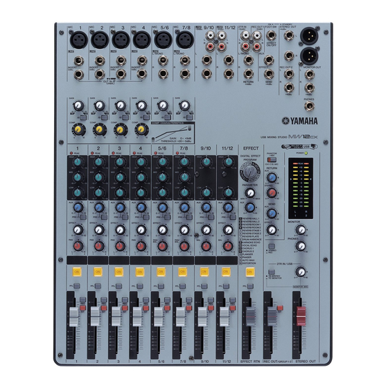
Page 8: Panel Layout (パネルレイアウト
MW12CX/MW12C PANEL LAYOUT (パネルレイアウト) • Channel Control Section (チャンネルコントロール部) MIC Input Jacks (CHs 1 to 4, 5/6, 7/8) Channels Channels Channels 1 to 4 5/6 and 7/8 9/10 and 11/12 LINE Input Jacks (CHs 1 to 4) (Monaural) (Stereo) (Stereo) - Page 9 MW12CX/MW12C • Master Control Section (マスターコントロール部) 2TR IN Jacks REC OUT 1 (L, R) Jacks REC OUT 2 (L, R) Jacks RETURN L (MONO), R Jacks SEND Jacks • AUX (AUX1) • EFFECT (AUX2) STEREO OUT (L, R) Jacks • XLR jacks •...
- Page 10 MW12CX/MW12C • Digital Effects Section (デジタルエフェクト部) * Only the MW12CX has digital effects. (この機能はMW12CX のみに内蔵されています。 ) FOOT SWITCH Jack PROGRAM Dial PARAMETER Control AUX Control ON Switch PFL Switch EFFECT RTN Fader FOOT SWITCH端子 PROGRAM選択ダイアル PARAMETERコントロール AUXコントロール ONスイッチ PFLスイッチ EFFECT RTNフェーダー...
- Page 11 MW12CX/MW12C • Connector Polarities • 端子接続の極性...
-
Page 12: Circuit Board Layout (ユニットレイアウト
MW12CX/MW12C CIRCUIT BOARD LAYOUT (ユニットレイアウト) (MW12CX) Rear (MW12C) (リア) PS12X (MW12CX) PS12 (MW12C) JK12UX (MW12CX) JK12U (MW12C) DSP2 (MW12CX only) MIX12UX (MW12CX) MIX12U (MW12C) Front (フロント)... -
Page 13: Wiring Diagram (基板結線図
(9P) (9P) (9P) (9P) (9P) (9P) (3P) (9P) (9P) (9P) (9P) CNM02 CN10 (5P) (20P) (20P) DSP2 (MW12CX only) MIX12UX (MW12CX) MIX12U (MW12C) Assembly Name Connection Remarks Part No. Location 線材名 接続 備考 USBMW12C束線 WJ914800 Connector Assembly JK12-CN10 <-> USB-CN101... -
Page 14: Mw12Cx Overall Assembly Wiring (Mw12Cx 総組立配線図
MW12CX/MW12C MW12CX MW12CX OVERALL ASSEMBLY WIRING (MW12CX 総組立配線図) The Wiring of the PS12X Circuit Board (PS12Xシートの配線) Connect the wires according to the following table and figure after installing the PS12X circuit board to the bottom case assembly. (ボトムケースAss’ yにPS12Xシートを取り付け後、下記の表/図に従い配線します。) Wiring point... - Page 15 MW12CX/MW12C MW12CX The Wiring of the JK12UX Circuit Board and MIX12UX Circuit Board (JK12UXシートとMIX12UXシートの配線) Install the JK12UX circuit board to the bottom case assembly. (JK12UXシートをボトムケースAss’ yに取り付けます。) Note) Pass the connector assembly USBMW12C through the incision part of the JK12UX circuit board as shown in the picture below.
- Page 16 MW12CX/MW12C MW12CX Install the MIX12UX circuit board to the bottom case assembly. (MIX12UXシートをボトムケースAss’ yに取り付けます。) Note) Put out the two connector assemblies PS124C and PS124CX through CN6 and CN8 as shown in the picture below. (下の写真のようにPS12Xに接続した線材をJK12UXシートとMIX12UXシートの間、CN6、CN8の間から出し ておきます。) Note) Take care not to pinch the two connector assemblies between the shield DSP2 and the JK12UX circuit board.
- Page 17 MW12CX/MW12C MW12CX Connect each CN1-CN8 on the JK12UX circuit board and MIX12UX circuit board using jumper wire. (JK12UXシートとMIX12UXシート上のそれぞれのCN1-CN8をジャンパーワイヤーで接続します。) JK12UX WJ540200 MIX12UX WJ540300 Bend the jumper-wires of CN1, CN2. (CN1、CN2のジャンパー線を折り曲げます。) a. Bend the Jumper-wires in the direction toward the MIX12UX circuit board.
- Page 18 MW12CX/MW12C MW12CX Bend the jumper-wires of CN3-CN8. (CN3-CN8のジャンパー線を折り曲げます。) a. Bend the Jumper-wires in the shape of “M” letter. (ジャンパー線を “M” 字形状に折り曲げます。) b. Process the Jumper-wires so that their height from the MIX12UX circuit board’s component side become 15 mm or less.
-
Page 19: Mw12C Overall Assembly Wiring (Mw12C 総組立配線図
MW12CX/MW12C MW12C MW12C OVERALL ASSEMBLY WIRING (MW12C 総組立配線図) The Wiring of the PS12 Circuit Board (PS12シートの配線) Connect the wires according to the following table and figure after installing the PS12 circuit board to the bottom case assembly. (ボトムケースAss’ yにPS12シートを取り付け後、下記の表/図に従い配線します。) Wiring point... - Page 20 MW12CX/MW12C MW12C The Wiring of the JK12U Circuit Board and MIX12U Circuit Board (JK12UシートとMIX12Uシートの配線) Install the JK12U circuit board to the bottom case assembly. (JK12UシートをボトムケースAss’ yに取り付けます。) Note) Pass the connector assembly USBMW12C through the incision part of the JK12U circuit board as shown in the picture below.
- Page 21 MW12CX/MW12C MW12C Install the MIX12U circuit board to the bottom case assembly. (MIX12UシートをボトムケースAss’ yに取り付けます。) Note) Put out the connector assembly PS124C through CN6 and CN8 as shown in the picture below. (下の写真のようにPS12に接続した線材をJK12UシートとMIX12Uシートの間、CN6、CN8の間から出してお きます。) Connect the wires according to the table below.
- Page 22 MW12CX/MW12C MW12C Connect each CN1-CN8 on the JK12U circuit board and MIX12U circuit board using jumper wire. (JK12UシートとMIX12Uシート上のそれぞれのCN1-CN8をジャンパーワイヤーで接続します。) JK12U WH109500 MIX12U WH109600 Bend the jumper-wires of CN1, CN2. (CN1、CN2のジャンパー線を折り曲げます。) a. Bend the Jumper-wires in the direction toward the MIX12U circuit board.
- Page 23 MW12CX/MW12C MW12C Bend the jumper-wires of CN3-CN8. (CN3-CN8のジャンパー線を折り曲げます。) a. Bend the Jumper-wires in the shape of “M” letter. (ジャンパー線を “M” 字形状に折り曲げます。) b. Process the Jumper-wires so that their height from the MIX12U circuit board’s component side become 15 mm or less.
-
Page 24: Mw12Cx Disassembly Procedures (Mw12Cx 分解手順
MW12CX/MW12C MW12CX I MW12CX DISASSEMBLY PROCEDURES (MW12CX 分解手順) トップカバー (所要時間:10分) Top Cover (Time required: 10 min.) Remove the eight (8) fader knobs marked [240], two (2) [240] のノブFADER8個、 [250] のノブFADER2個、 fader knobs marked [250], fader knob marked [260] and [260] のノブFADER、 [300] のノブSELECTを外しま... - Page 25 MW12CX/MW12C MW12CX MIX12UXシート、DSP2シート、JK12UXシー MIX12UX Circuit Board, DSP2 Circuit Board and JK12UX Circuit Board ト (所要時間:15分) (Time required: 15 min.) トップカバーを外します。 (1項参照) [120] のネジ7本、 [130] の6角スペーサーを外します。 Remove the top cover. (See procedure 1.) (Fig. 2) Remove the seven (7) screws marked [120] and hex- 11ヶ所のコネクターを外します。...
- Page 26 MW12CX/MW12C MW12CX PS12Xシート (所要時間:15分) PS12X Circuit Board (Time required: 15 min.) トップカバーを外します。 (1項参照) Remove the top cover. (See procedure 1.) MIX12UXシート、DSP2シート、JK12UXシートを外し ます。 (2項参照) Remove the MIX12UX circuit board, DSP2 circuit board and JK12UX circuit board. (See procedure 2.) [183] のネジを外します。3ヶ所のフックを外し、PS12X シート...
-
Page 27: Mw12C Disassembly Procedures (Mw12C 分解手順
MW12CX/MW12C MW12C I MW12C DISASSEMBLY PROCEDURES (MW12C 分解手順) トップカバー (所要時間:10分) Top Cover (Time required: 10 min.) Remove the eight (8) fader knobs marked [240], fader [240] のノブFADER8個、 [250] のノブFADER、 [260] の knob marked [250] and fader knob marked [260]. (Fig. 1) ノブFADERを外します。... - Page 28 MW12CX/MW12C MW12C MIX12Uシート、JK12Uシート MIX12U Circuit Board and JK12U Circuit Board (Time required: 15 min.) (所要時間:15分) Remove the top cover. (See procedure 1.) トップカバーを外します。 (1項参照) Remove the seven (7) screws marked [120]. (Fig. 2) [120] のネジ7本を外します。 (Fig. 2) Disconnect the ten (10) connectors.
- Page 29 MW12CX/MW12C MW12C PS12シート (所要時間:15分) PS12 Circuit Board (Time required: 15 min.) Remove the top cover. (See procedure 1.) トップカバーを外します。 (1項参照) Remove the MIX12U circuit board and JK12U circuit MIX12Uシート、JK12Uシートを外します。 (2項参照) board. (See procedure 2.) [183] のネジを外します。3ヶ所のフックを外し、PS12 Remove the screw marked [183].
-
Page 30: Lsi Pin Description (Lsi端子機能表
MW12CX/MW12C LSI PIN DESCRIPTION (LSI端子機能表) • AK5381VT-E2 (X5219A00) ADC (Analog to Digital Converter) DSP2: ICM04 NAME FUNCTION NAME FUNCTION AINR Rch analog input pin SDTO Audio serial data output pin AINL Lch analog input pin LRCK Output channnel clock pin... - Page 31 MW12CX/MW12C • YMW767-VTZ (X6055A00) CPU (SWLO1B) DSP2: ICM07 NAME FUNCTION NAME FUNCTION Ground Ground TESTN Input for test Power supply +3.3 V PLLBPN PLL bypass select LBN/LWRN/PF6 External memory lower-byte enable / Port F PLLV PLL power supply +2.5 V...
-
Page 32: Ic Block Diagram (Icブロック図
MW12CX/MW12C IC BLOCK DIAGRAM (IC ブロック図) • PST596DNR (X0165A00) System Reset DSP2: ICM03 Delay – – • NJM2068M-D (TE2) (X3505A00) • KIA7812API (X4153A00) Dual Operational Amplifier Regulator +12V JACK12: IC202, 302 PS12: IC03 MIX12: IC701, 751, 801, 851 USB: IC103, 104... - Page 33 MW12CX/MW12C • KIA7805API/P (X4928A00) • KIA7815API (X4930A00) Regulator +5V Regulator +15V PS12: IC04 (MW12CX), IC05 PS12: IC01 INPUT INPUT Q11-1 Q11-1 OUTPUT OUTPUT COMMON (GND) COMMON (GND) • KIA7915PI (X4931A00) Regulator -15V PS12: IC02 R 21 R 16 Q 23...
- Page 34 ICM09, 11 IC401, 501, 601, 651, 851 JACK12: IC004, 104 MIX12: IC001, 002, 101, 102, 201, 202 MIX12: IC852, 901, 951 (MW12CX) IC301, 302, 401, 402, 501, 502 IC702, 703, 752, 802, 853 OUT2 - IN2 + IN2 2, 6 –INPUT...
-
Page 35: Circuit Boards (シート基板図
• USB Circuit Board (X7196C0) ........... 35 Note: See parts list for details of circuit board component parts. 注 : シートの部品詳細はパーツリストをご参照ください。 • DSP2 Circuit Board (MW12CX only) to MIX12 CN10 Component side (部品側) Pattern side (パターン側) 2NA-WH10870 • USB Circuit Board... - Page 36 MW12CX/MW12C MW12CX MW12C • JK12UX/JK12U Circuit Board to M to MIX12 CN1 to MIX12 CN2 to MIX12 CN3 Component side (部品側) 2NA-WH10890...
- Page 37 MW12CX/MW12C MW12CX MW12C to MIX12 CN4 to MIX12 CN5 to MIX12 CN6 to PS CN02 to MIX12 CN7 to MIX12 CN8 to USB CN101 Component side (部品側) 2NA-WH10890...
- Page 38 MW12CX/MW12C MW12CX MW12C • JK12UX/JK12U Circuit Board Pattern side (パターン側) 2NA-WH10890...
- Page 39 MW12CX/MW12C MW12CX MW12C Pattern side (パターン側) 2NA-WH10890...
- Page 40 MW12CX/MW12C MW12CX MW12C • MIX12UX/MIX12U Circuit Board to JK1 to JK12 CN1 to JK12 CN2 to JK12 CN3 Reduction: 4/5 Component side (部品側) 2NA-WH10900...
- Page 41 MW12CX/MW12C MW12CX MW12C to JK12 CN7 to JK12 CN4 to JK12 CN5 to JK12 CN6 to DSP2 CNM02 to PS12 CN03 to JK12 CN8 9/10 11/12 EFFECT Reduction: 4/5 Component side (部品側) 2NA-WH10900...
- Page 42 MW12CX/MW12C MW12CX MW12C • MIX12UX/MIX12U Circuit Board Reduction: 4/5 Pattern side (パターン側) 2NA-WH10900...
- Page 43 MW12CX/MW12C MW12CX MW12C Reduction: 4/5 Pattern side (パターン側) 2NA-WH10900...
- Page 44 MW12CX/MW12C MW12CX MW12C • PS12X/PS12 Circuit Board to JK12 CN9 to MIX12 CN9 AC ADAPTOR IN STANDBY ON Component side (部品側) 28CA1-WH10910...
-
Page 45: Inspections (検査
80 switch COMP control Minimum EQ (HIGH, MID, LOW) GAIN control CENTER AUX1, AUX2 level control (MW12C) Maximum AUX, EFFECT level control (MW12CX) Maximum AUX1 PRE switch (MW12C) OFF (POST) AUX PRE switch (MW12CX) OFF (POST) PAN control L (turned counterclockwise fully) - Page 46 REC OUT/GROUP1-2 TO ST ASSIGN switch STEREO Master fader (STEREO) Maximum AUX1, AUX2 SEND Master level control (MW12C) Maximum AUX, EFFECT SEND Master level control (MW12CX) Maximum RETURN TO AUX1, ST level control (MW12C) Maximum RETURN TO AUX, ST level control (MW12CX)
- Page 47 10R, 12R Table 2-6-5 Input Terminal RETURN L, R INPUT ST OUT AUX1 SEND (MW12C) INPUT LEVEL AUX SEND (MW12CX) +16 ± 2 dBu +16 ± 2 dBu +15 ± 2 dBu L/MONO 0 dBu +16 ± 2 dBu +9 ± 2 dBu...
- Page 48 MW12CX/MW12C Frequency Characteristic In the signal route 1 to 0 specified in the table 2-6-1 to 2-6-6, check the 20 Hz and 20 kHz frequency response of each output is within the range of +1/-2.5 dB compared with the 1 kHz (0 dB).
- Page 49 Check the distortion is 1 % or less when the output level obtained at REC OUT2, AUX1, 2 SEND (MW12C), AUX, EFFECT, SEND (MW12CX) and MONITOR OUT is +20 dBu. Check the distortion is 1 % or less when the output level obtained at PHONES (L, R) is +7.5 dBu.
- Page 50 MW12CX/MW12C 2-17 COMP 2-17-1 GAIN With controls set as specified in the section 2-2, set the COMP control of channels 1-4 to maximum. Then check the output level obtained at INSERT OUT 1-4 is within the range specified in the table 2-17-1.
- Page 51 MW12CX/MW12C 2-18 DIGITAL EFFECT (MW12CX) Set the CH1 as follows and input -60 dBu signal to CH1 MIC. Set EFFECT RTN fader and EFFECT RTN AUX VR to maximum and check the output level is the value specified in the Table 2-18.
- Page 52 MW12CX/MW12C Others Execute each test with controls set effective. Effect (MW12CX only) Check the effect program [1], [6], [11] and [16] are effective respectively. Check the output signal can be controlled with the parameter volume in each effect program. Check the allophone can not be heard when the program is changed.
- Page 53 80 スイッチ COMPコントロール 最小 EQ (HIGH、MID、LOW) GAINコントロール CENTER AUX1、AUX2レベルコントロール (MW12C) 最大 AUX、EFFECTレベルコントロール (MW12CX) 最大 AUX1 PREスイッチ (MW12C) OFF ( POST) AUX PREスイッチ (MW12CX) OFF ( POST) PANコントロール L ( 反時計方向一杯に回します。) ONスイッチ 測定時ON (LEDが点灯します。) 、他はOFF PFLスイッチ 測定時ON、他はOFF RECスイッチ 測定時ON、他はOFF STスイッチ 測定時ON、他はOFF チャンネルフェーダー...
- Page 54 OFF ( POST) BALコントロール L ( 反時計方向一杯に回します。) ONスイッチ 測定時ON (LEDが点灯します。) 、他はOFF PFLスイッチ 測定時ON、他はOFF RECスイッチ 測定時ON、他はOFF STスイッチ 測定時ON、他はOFF チャンネルフェーダー 最大 ・ DIGITAL EFFECT (MW12CX) PROGRAM選択ダイアル PARAMETERコントロール 最小 AUXレベルコントロール 測定時のみ最大、他は最小 ONスイッチ 測定時ON (LEDが点灯します。) 、他はOFF PFLスイッチ 測定時ON、他はOFF EFFECT RTNフェーダー 測定時のみ最大、他は最小 ・ MASTERコントロール REC OUT/GROUP1-2マスターフェーダー (STEREO)...
- Page 55 10R, 12R 表2-6-5 入力端子 RETURN L、R INPUT ST OUT AUX1 SEND (MW12C) INPUT LEVEL AUX SEND (MW12CX) +16 ± 2 dBu +16 ± 2 dBu +15 ± 2 dBu L/MONO 0 dBu +16 ± 2 dBu +9 ± 2 dBu 表2-6-6 入力端子...
- Page 56 MW12CX/MW12C 周波数特性 表2-6-1∼6 ( ①∼⑩) の信号系統において、入力信号周波数を20 Hz、20 kHzとした時、各出力端子の出力レベルは1 kHzを基 準として、+1.0/-2.5 dBの範囲内にあることを確認します。 * GAINコントロール最大時の20 Hzのみ、+1.0 dB、-4.5 dBとします。 * ①の系統は、CH1のみ全部のOUTで確認し、CH2以降はST L OUTのみ確認します。 * ④の系統は、ST L OUT、ST R OUTのみ確認します。 表2.6.1、表2.6.2で指定された設定状態で、GAINコントロ−ルを最小にして80 Hz、-36 dBuの信号を入力します。 80 スイッ チをONした時、ST L OUTの出力レベルは 80 スイッチがOFF時のレベルを基準に-3±2 dBの範囲内にあることを確認しま す。 チャンネルEQ変化特性 2-2の項で指定された設定状態で、各EQゲインコントロール (HIGH、MID、LOW) をそれぞれ動かした時、REC OUT2 Lと...
- Page 57 * ⑫の系統は、INSERT OUTに+10 dBuの出力が得られた時の歪率は0.1 %以下であることを確認します。 * 測定しない出力のMaser Level controlとFaderはMINにしておきます。 2-14 最大出力 2-2の項で指定された設定状態で、ST OUTに+24 dBuの出力が得られた時、歪率が1 %以下であることを確認します。 REC OUT2、AUX1, 2 SEND (MW12C) 、AUX, EFFECT SEND (MW12CX) 、MONITOR OUTに+20 dBuの出力が得られた時、 歪率が1 %以下であることを確認します。 PHONES ( L、R) に+7.5 dBuの出力が得られた時、歪率が1 %以下であることを確認します。 注意: ・ ST OUT、REC OUT2測定時は、PANまたはPAN/BALコントロールをLまたはRに廻しきります。...
- Page 58 MW12CX/MW12C 2-17 COMP 2-17-1 ゲイン 2-2の項で指定された設定状態で、チャンネル1-4のCOMPコントロールを最大に設定した時、各INSERT OUTに得られる出 力レベルは、表2-17-1の範囲内にあることを確認します。 表2-17-1 CH INPUT 1-4 INPUT LEVEL COMPコントロール INSERT OUT 1-4 +3 ± 2 dBu 最大 INPUT A -65 dBu 2-17-2 レシオ 入力レベルを+10 dB上げた時、INSERT OUT 1-4に得られる出力レベルは、2-17-1の出力レベルを基準として、表2-17-2の範 囲内にあることを確認します。 表2-17-2 CH INPUT 1-4 INPUT LEVEL INSERT OUT 1-4 +3.5 ±...
- Page 59 MW12CX/MW12C 2-18 デジタルエフェクト (MW12CX) CH1を次のように設定し、CH1 MICに-60 dBuの信号を入力します。 EFFECT RTNフェーダーとEFFECT RTN AUX VRをMAXにしたとき、表2-18の出力レベルが得られることを確認します。 ***CH1*** GAIN VR、AUX VR : 最小 フェーダー、EFFECT VR : 最大 ON switch : ON PFL switch : OFF 表2-18 STフェーダー PROGRAM select AUX SENDボリューム PARAMETER OUTPUT level OUTPUT...
- Page 60 MW12CX/MW12C その他 それぞれの操作子類を有効な設定にした上で各部の確認を行ってください。 エフェクト (MW12CX) ・ エフェクトプログラムの [1] 、 [6] 、 [11] 、 [16] それぞれにおいて、プログラム効果が確認できること。 ・ それぞれのプログラムにおいて、パラメータボリュームを操作して変化が確認できること。 ・ プログラム切り替え時に異音のないこと。 ファンタム電源 ・ INPUT AまたはMIC入力コネクタのピン1-2間に負荷抵抗10 kΩを接続し、ピン2-3間を短絡します。 ・ PHANTOMスイッチをオンした時、PHNATOMインジケータが点灯し負荷抵抗両端に+33.0 V∼+37.0 Vの電圧が得られる こと。 出荷設定 工場出荷時の設定 ・ EQ GAINコントロール (HIGHT、MID、LOW):センター (0) ・ PAN、BAL、PAN/BALコントロール :センター ・ その他のVRコントロール...
-
Page 61: Parts List
MW12CX/MW12C PARTS LIST I CONTENTS (目次) MW12CX OVERALL ASSEMBLY (MW12CX 総組立)......2 MW12C OVERALL ASSEMBLY (MW12C 総組立)....... 4 ELECTRICAL PARTS (電気部品) ............6 Notes: DESTINATION ABBREVIATIONS Australian model South African model British model Chinese model Canadian model South-east Asia model... - Page 62 MW12CX/MW12C MW12CX MW12CX OVERALL ASSEMBLY (MW12CX 総組立) Accessories of Phone Jack Accessories of Phone Jack (ホーンジャック付属品) (ホーンジャック付属品) Screw tighten (1st) (ネジ締め (1番) ) Screw tighten (latest) (ネジ締め (最後) ) Screw tighten (2nd) (ネジ締め (2番) ) Priority tighten in 30 (30の内で最初にネジ締め)...
- Page 63 MW12CX/MW12C MW12CX PART NO. DESCRIPTION 部 品 名 REMARKS REF NO. RANK OVERALL ASSEMBLY 総 組 立 MW12CX Overall Assembly 総 組 立 (WJ94990) WJ968900 Bottom Case Assembly ボ ト ム ケ ー ス A s s ’ y Bottom Case ボ...
- Page 64 MW12CX/MW12C MW12C MW12C OVERALL ASSEMBLY (MW12C 総組立) Accessories of Phone Jack Accessories of Phone Jack (ホーンジャック付属品) (ホーンジャック付属品) Screw tighten (1st) (ネジ締め (1番) ) Screw tighten (2nd) (ネジ締め (2番) ) Priority tighten in 30 (30の内で最初にネジ締め) AC Adaptor (J) OUTPUT: AC35VCT 0.94A...
- Page 65 MW12CX/MW12C MW12C PART NO. DESCRIPTION 部 品 名 REMARKS REF NO. RANK OVERALL ASSEMBLY 総 組 立 MW12C Overall Assembly 総 組 立 (WJ95000) WJ968900 Bottom Case Assembly ボ ト ム ケ ー ス A s s ’ y Bottom Case ボ...
-
Page 66: Electrical Parts
MW12CX/MW12C MW12CX MW12C ELECTRICAL PARTS (電気部品) PART NO. DESCRIPTION 部 品 名 REMARKS REF NO. RANK ELECTRICAL PARTS 電 気 部 品 MW12CX WJ940000 Circuit Board DSP2 D S P 2 シ ー ト (WJ93990)(X7687D0) WJ540200 Circuit Board JK12UX J K 1 2 U X シ ー ト... - Page 67 MW12CX/MW12C MW12CX MW12C DSP2 and JK12UX/JK12U PART NO. DESCRIPTION 部 品 名 REMARKS REF NO. RANK ICM08 X3538A00 PCM1742KEG/2K I C ICM09 X7378A00 NJM4565M(TE1) I C OP AMP ICM10 X5922A00 MX23L8103TC-90G I C ICM11 X7378A00 NJM4565M(TE1) I C OP AMP...
- Page 68 MW12CX/MW12C MW12CX MW12C JK12UX/JK12U PART NO. DESCRIPTION 部 品 名 REMARKS REF NO. RANK C009 WH167700 Electrolytic Cap. 10uF ケ ミ コ ン C010 WH167700 Electrolytic Cap. 10uF ケ ミ コ ン C011 UR867100 Electrolytic Cap. 10uF ケ ミ コ...
- Page 69 MW12CX/MW12C MW12CX MW12C JK12UX/JK12U PART NO. DESCRIPTION 部 品 名 REMARKS REF NO. RANK C119 UR867100 Electrolytic Cap. 10uF ケ ミ コ ン C120 UR838220 Electrolytic Cap. 220uF 16V ケ ミ コ ン } C121 US064100 Ceramic Capacitor-B (chip) 0.01uF 50V K チ...
- Page 70 MW12CX/MW12C MW12CX MW12C JK12UX/JK12U PART NO. DESCRIPTION 部 品 名 REMARKS REF NO. RANK C303 WH167700 Electrolytic Cap. 10uF ケ ミ コ ン C304 WH167700 Electrolytic Cap. 10uF ケ ミ コ ン C305 UR867100 Electrolytic Cap. 10uF ケ ミ コ...
- Page 71 MW12CX/MW12C MW12CX MW12C JK12UX/JK12U PART NO. DESCRIPTION 部 品 名 REMARKS REF NO. RANK C753 US061330 Ceramic Capacitor-CH(chip) 33pF 50V J チ ッ プ セ ラ( C H ) -756 US061330 Ceramic Capacitor-CH(chip) 33pF 50V J チ ッ プ セ ラ( C H )...
- Page 72 MW12CX/MW12C MW12CX MW12C JK12UX/JK12U PART NO. DESCRIPTION 部 品 名 REMARKS REF NO. RANK D152 VR496500 Diode (chip) MA111 FLAT TP チ ッ プ ダ イ オ ー ド D152 VT332900 Diode 1SS355 TE-17 ダ イ オ ー...
- Page 73 MW12CX/MW12C MW12CX MW12C JK12UX/JK12U PART NO. DESCRIPTION 部 品 名 REMARKS REF NO. RANK Q002 V 7 4 2 1 7 0 0 Transistor (chip) 2SC3324 GR,BL チ ッ プ ト ラ ン ジ ス タ Q003 WH249200 2SK208-GR(TE85L,F) F...
- Page 74 MW12CX/MW12C MW12CX MW12C JK12UX/JK12U PART NO. DESCRIPTION 部 品 名 REMARKS REF NO. RANK R069 RF356820 Metal Film Resistor (chip) 8.2K 1/16W D チ ッ プ 金 被 抵 抗 R070 RF356220 Metal Film Resistor (chip) 2.2K 1/16W D チ ッ プ 金 被 抵 抗...
- Page 75 MW12CX/MW12C MW12CX MW12C JK12UX/JK12U PART NO. DESCRIPTION 部 品 名 REMARKS REF NO. RANK R169 RF356820 Metal Film Resistor (chip) 8.2K 1/16W D チ ッ プ 金 被 抵 抗 R170 RF356220 Metal Film Resistor (chip) 2.2K 1/16W D チ ッ プ 金 被 抵 抗...
- Page 76 MW12CX/MW12C MW12CX MW12C JK12UX/JK12U PART NO. DESCRIPTION 部 品 名 REMARKS REF NO. RANK R324 RD354470 Carbon Resistor (chip) 1/16W J チ ッ プ 抵 抗 R325 RD354470 Carbon Resistor (chip) 1/16W J チ ッ プ 抵 抗 R326 RD357150...
- Page 77 MW12CX/MW12C MW12CX MW12C JK12UX/JK12U and MIX12UX/MIX12U PART NO. DESCRIPTION 部 品 名 REMARKS REF NO. RANK R763 RF357200 Metal Film Resistor (chip) 20K 1/16W D チ ッ プ 金 被 抵 抗 R764 RF357180 Metal Film Resistor (chip) 18K 1/16W D チ...
- Page 78 MW12CX/MW12C MW12CX MW12C MIX12UX/MIX12U PART NO. DESCRIPTION 部 品 名 REMARKS REF NO. RANK C015 UR857470 Electrolytic Cap. 47uF ケ ミ コ ン C016 US064100 Ceramic Capacitor-B (chip) 0.01uF 50V K チ ッ プ セ ラ ( B ) C017...
- Page 79 MW12CX/MW12C MW12CX MW12C MIX12UX/MIX12U PART NO. DESCRIPTION 部 品 名 REMARKS REF NO. RANK C219 UR867100 Electrolytic Cap. 10uF ケ ミ コ ン C220 UR867100 Electrolytic Cap. 10uF ケ ミ コ ン C223 US062100 Ceramic Capacitor-SL(chip) 100pF 50V J チ ッ プ セ ラ( S L )...
- Page 80 MW12CX/MW12C MW12CX MW12C MIX12UX/MIX12U PART NO. DESCRIPTION 部 品 名 REMARKS REF NO. RANK C510 US062100 Ceramic Capacitor-SL(chip) 100pF 50V J チ ッ プ セ ラ( S L ) C511 UR857470 Electrolytic Cap. 47uF ケ ミ コ ン C512 UR857470 Electrolytic Cap.
- Page 81 MW12CX/MW12C MW12CX MW12C MIX12UX/MIX12U PART NO. DESCRIPTION 部 品 名 REMARKS REF NO. RANK C851 US063100 Ceramic Capacitor-B (chip) 1000pF 50V K チ ッ プ セ ラ ( B ) C852 US062220 Ceramic Capacitor-SL(chip) 220pF 50V J チ ッ プ セ ラ( S L )...
- Page 82 MW12CX/MW12C MW12CX MW12C MIX12UX/MIX12U PART NO. DESCRIPTION 部 品 名 REMARKS REF NO. RANK IC402 X6897A00 BA4560RF-E2 OPAMP I C OP AMP IC501 X6897A00 BA4560RF-E2 OPAMP I C OP AMP IC502 X6897A00 BA4560RF-E2 OPAMP I C OP AMP IC701 X3505A00 NJM2068M-D(TE2) I...
- Page 83 MW12CX/MW12C MW12CX MW12C MIX12UX/MIX12U PART NO. DESCRIPTION 部 品 名 REMARKS REF NO. RANK Q302 VV556500 Transistor 2SA1037AK Q,R,S ト ラ ン ジ ス タ Q302 WC529500 Transistor KTA1504S-Y,GR-RTK/ ト ラ ン ジ ス タ Q501...
- Page 84 MW12CX/MW12C MW12CX MW12C MIX12UX/MIX12U PART NO. DESCRIPTION 部 品 名 REMARKS REF NO. RANK R120 RD356680 Carbon Resistor (chip) 6.8K 1/16W J チ ッ プ 抵 抗 R121 RD357150 Carbon Resistor (chip) 15K 1/16W J チ ッ プ 抵 抗...
- Page 85 MW12CX/MW12C MW12CX MW12C MIX12UX/MIX12U PART NO. DESCRIPTION 部 品 名 REMARKS REF NO. RANK R306 RD356270 Carbon Resistor (chip) 2.7K 1/16W J チ ッ プ 抵 抗 R307 RD357100 Carbon Resistor (chip) 10K 1/16W J チ ッ プ 抵 抗...
- Page 86 MW12CX/MW12C MW12CX MW12C MIX12UX/MIX12U PART NO. DESCRIPTION 部 品 名 REMARKS REF NO. RANK R519 RD357330 Carbon Resistor (chip) 33K 1/16W J チ ッ プ 抵 抗 R522 RD356680 Carbon Resistor (chip) 6.8K 1/16W J チ ッ プ 抵 抗...
- Page 87 MW12CX/MW12C MW12CX MW12C MIX12UX/MIX12U PART NO. DESCRIPTION 部 品 名 REMARKS REF NO. RANK R901 RD357220 Carbon Resistor (chip) 22K 1/16W J チ ッ プ 抵 抗 R902 RD357220 Carbon Resistor (chip) 22K 1/16W J チ ッ プ 抵 抗...
- Page 88 MW12CX/MW12C MW12CX MW12C MIX12UX/MIX12U PART NO. DESCRIPTION 部 品 名 REMARKS REF NO. RANK SW002 WH918700 Push Switch PS-22E85L-02 プ ッ シ ュ S W PFL(CH1) SW003 WH918700 Push Switch PS-22E85L-02 プ ッ シ ュ S W PRE(CH1) SW004 WH918700...
- Page 89 ロ ー タ リ ー V R VR801 V 8 2 6 4 6 0 0 Rotary Variable Resistor A 20K XV09213YNP SEND MASTER AUX(MW12CX) SEND MASTER AUX1(MW12C) ロ ー タ リ ー V R VR802 V 8 2 6 4 6 0 0...
- Page 90 IC03 X4153A00 KIA7812API I C REGULATOR +12V I C IC04 X4928A00 KIA7805API/P REGULATOR +5V (MW12CX) IC05 X4928A00 KIA7805API/P I C REGULATOR +5V GND Plate MLA8 プ レ ー ト G N D (WC53340) ス タ イ ル ピ ン L = 3 5...
- Page 91 MW12CX/MW12C MW12CX MW12C PART NO. DESCRIPTION 部 品 名 REMARKS REF NO. RANK C111 US063680 Ceramic Capacitor-B(chip) 6800pF 50V K チ ッ プ セ ラ ( B ) C112 US063680 Ceramic Capacitor-B(chip) 6800pF 50V K チ ッ プ セ ラ ( B )...
-
Page 92: Circuit Diagram
MW12CX/MW12C CIRCUIT DIAGRAM I CONTENTS (目次) IC & DIODE FIGURES (外形図)................ 2 BLOCK & LEVEL DIAGRAM (ブロック&レベルダイアグラム) ......3 CIRCUIT DIAGRAM (回路図) DSP2 ......................4 JK12UX/JK12U 1/4 ..................5 JK12UX/JK12U 2/4 ..................6 JK12UX/JK12U 3/4 ..................7 JK12UX/JK12U 4/4 ..................8 MIX12UX/MIX12U 1/5 .................. -
Page 93: Ic & Diode Figures (外形図
MW12CX/MW12C IC & DIODE FIGURES (外形図) • TAR5S33 (XZ642A00) • KIA7815API (X4930A00) • KIA7915PI (X4931A00) • TAR5S25U (X8138A00) REGULATOR +3.3V REGULATOR +15V REGULATOR -15V REGULATOR +2.5V DSP2: ICM06 PS12: IC01 PS12: IC02 DSP2: ICM12 VOUT VOUT CONT CONT 1: GND... -
Page 94: Block & Level Diagram (ブロック&レベルダイアグラム
ST CH Level [Nominal:-6dB] [Nominal:-10dB] [Nominal:-10dB] -20 d Bu -20 d Bu [-10dBu] [Nominal:-10dB] ST CH AUX, EFFECT(MW12CX) [Nominal:-6dB] MONITOR [Nominal:-6dB] [Nominal:-6dB] PHONES [Nominal:-16dB] -30 d Bu -30 d Bu CH IN LINE Gain:Max [-34dBu] ST CH IN LINE Gain:Max [-34dBu]... - Page 95 MW12CX/MW12C CIRCUIT DIAGRAM 1/12 (DSP2) MW12CX only SYSTEM RESET JTAG Mounted Not mounted JTAG Not mounted Mounted OP AMP OP AMP to MX12U_CN10 REGULATOR +3.3V <P. 13: F3> Components marked XX are not installed. XX :未実装 (セ) : Ceramic Capacitor (セラミックコンデンサー)...
- Page 96 MW12CX/MW12C CIRCUIT DIAGRAM 2/12 (JK12UX/JK12U 1/4) MW12CX MW12C <2/4: K1, 4/4: K4> OP AMP OP AMP to MIX12_CN1 <P. 9: P3> OP AMP OP AMP OP AMP OP AMP to MIX12_CN2 <P. 9: P8> OP AMP OP AMP (セ) :...
- Page 97 MW12CX/MW12C CIRCUIT DIAGRAM 3/12 (JK12UX/JK12U 2/4) MW12CX MW12C <1/4: O1, 4/4: K4> OP AMP OP AMP OP AMP to MIX12_CN3 <P. 10: P4> OP AMP (セ) : Ceramic Capacitor (セラミックコンデンサー) : Electrolytic Capacitor (ケミカルコンデンサー) (LL) : Electrolytic Capacitor (ケミカルコンデンサー) (マ)...
- Page 98 MW12CX/MW12C CIRCUIT DIAGRAM 4/12 (JK12UX/JK12U 3/4) MW12CX MW12C OP AMP OP AMP OP AMP to MIX12_CN4 <P. 11: O3> <4/4: K2> <4/4: K2> OP AMP JK12UX only installed <4/4: K7> <4/4: K8> installed OP AMP to MIX12_CN5 <P. 12: H5>...
- Page 99 MW12CX/MW12C CIRCUIT DIAGRAM 5/12 (JK12UX/JK12U 4/4) MW12CX MW12C <3/4: B5> <3/4: B5> OP AMP <3/4: E2> OP AMP OP AMP OP AMP <3/4: E2> to USB_CN101 <P. 15: E6> <1/4: O1, 2/4: K1> OP AMP to MIX12_CN6 <P. 12: H4>...
- Page 100 MW12CX/MW12C CIRCUIT DIAGRAM 6/12 (MIX12UX/MIX12U 1/5) MW12CX MW12C <2/5: B2, 3/5: B1, 4/5: P4, 5/5: A2> <2/5: B2, 3/5: B2, 4/5: P5, 5/5: A3> OP AMP MW12CX MW12C <2/5: B3, 3/5: B2, 4/5: P2> OP AMP <2/5: B3, 3/5: B2, 4/5: P2>...
- Page 101 MW12CX/MW12C CIRCUIT DIAGRAM 7/12 (MIX12UX/MIX12U 2/5) MW12CX MW12C <1/5: C1, 3/5: B1, 4/5: P4, 5/5: A2> <1/5: C2, 3/5: B2, 4/5: P5, 5/5: A3> OP AMP <1/5: C2, 3/5: B2, 4/5: P2> OP AMP <1/5: C2, 3/5: B2, 4/5: P2>...
- Page 102 MW12CX/MW12C CIRCUIT DIAGRAM 8/12 (MIX12UX/MIX12U 3/5) MW12CX MW12C <2/5: I10> <1/5: C1, 2/5: B2, 4/5: P4, 5/5: A2> <1/5: C2, 2/5: B2, 4/5: P5, 5/5: A3> OP AMP <1/5: C2, 2/5: B3, 4/5: P2> OP AMP <1/5: C2, 2/5: B3, 4/5: P2>...
- Page 103 MW12CX/MW12C CIRCUIT DIAGRAM 9/12 (MIX12UX/MIX12U 4/5) MW12CX MW12C <1/5: C2, 2/5: B3, 3/5: B2> OP AMP OP AMP OP AMP OP AMP OP AMP <1/5: C2, 2/5: B3, 3/5: B2> COMPARATOR to JK12_CN6 <P. 8: G4> <1/5: C1, 2/5: B2, 3/5: B1, 5/5: A2>...
- Page 104 MW12CX/MW12C CIRCUIT DIAGRAM 10/12 (MIX12UX/MIX12U 5/5) MW12CX only <1/5: C1, 2/5: B2, 3/5: B1, 4/5: P4> OP AMP to PS12_CN03 <P. 14: A4> <1/5: C2, 2/5: B2, 3/5: B2, 4/5: P5> <4/5: P5> OP AMP <1/5: C3, 2/5: B5, 3/5: B4, 4/5: P7>...
- Page 105 MW12CX/MW12C CIRCUIT DIAGRAM 11/12 (PS12X/PS12) MW12CX MW12C REGULATOR +15V REGULATOR -15V to JK12_CN9 REGULATOR +12V <P. 8: K6> (MW12CX only) REGULATOR +5V to MIX12_CN9 <P. 13: F2> REGULATOR +5V Installed 実装 非実装 Not installed (セ) : Ceramic Capacitor (セラミックコンデンサー) :...
- Page 106 MW12CX/MW12C CIRCUIT DIAGRAM 12/12 (USB) MW12CX MW12C REGULATOR CODEC OP AMP OP AMP Components marked XX are not installed. OP AMP XX :未実装 (セ) : Ceramic Capacitor (セラミックコンデンサー) : Electrolytic Capacitor (ケミカルコンデンサー) (D) : Metal Film Resistor (金属被膜抵抗) Note : See parts list for details of circuit board component parts.
Need help?
Do you have a question about the MW12CX and is the answer not in the manual?
Questions and answers