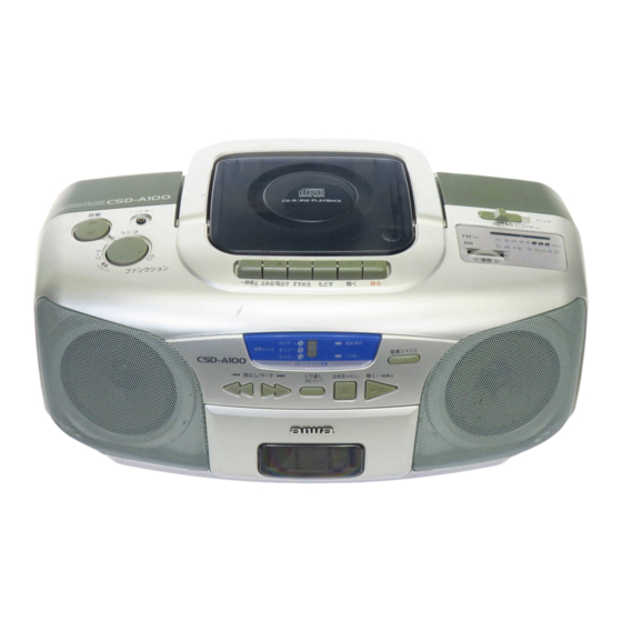
Aiwa csd-a100 Service Manual
Compact disc stereo cassette receiver
Hide thumbs
Also See for csd-a100:
- Service manual (25 pages) ,
- Service manual (20 pages) ,
- Service manual (28 pages)
Advertisement
Table of Contents
- 1 Specifications
- 2 Accessories/Package List
- 3 Protection of Eyes from Laser Beam During Servicing
- 4 Precaution to Replace Optical Block
- 5 Electrical Main Parts List
- 6 IC Block Diagram
- 7 Transistor Illustration
- 8 Practical Service Figure
- 9 Tuner Section
- 10 Mechanical Parts List
- 11 Color Name Table
- 12 Mechanical Exploded View
- 13 Tape Mechanism Exploded View
- 14 Tape Mechanism Parts List
- 15 CD Mechanism Exploded View
- Download this manual
Advertisement
Table of Contents

Subscribe to Our Youtube Channel
Related Manuals for Aiwa csd-a100


Summary of Contents for Aiwa csd-a100
- Page 1 CSD-A100 G(S),V(S) SERVICE MANUAL COMPACT DISC STEREO BASIC TAPE MECHANISM : ZZM-1 YR2NP CASSETTE RECEIVER BASIC CD MECHANISM : DA11T3C This Service Manual is the "Revision Publishing" and replaces "Simple Manual" (S/M Code No. 09-003-342-2T6). S/M Code No. 09-003-342-2R6...
-
Page 2: Specifications
SPECIFICATIONS GSC MODEL VSC MODEL • Design and specifications are subject to change without • Design and specifications are subject to change without notice notice ACCESSORIES/PACKAGE LIST REF. NO PART NO. KANRI DESCRIPTION 1 8A-CDA-904-010 IB,G(E)FM<GSC> 1 8A-CDA-907-010 IB,V(ER)FM<VSC> 2 87-050-076-010 AC CORD SET ASSY,E<VSC>... -
Page 3: Protection Of Eyes From Laser Beam During Servicing
PROTECTION OF EYES FROM LASER BEAM DURING SERVICING This set employs laser. Therefore, be sure to follow carefully the CAUTION instructions below when servicing. Use of controls or adjustments or performance of procedures other than those specified herein may result in hazardous WARNING! radiation exposure. -
Page 4: Electrical Main Parts List
ELECTRICAL MAIN PARTS LIST REF. NO PART NO. KANRI DESCRIPTION REF. NO PART NO. KANRI DESCRIPTION C816 87-010-180-080 C-CER 1500P C817 87-010-180-080 C-CER 1500P 87-A20-955-010 IC,LA1828 C821 87-010-401-080 CAP, ELECT 1-50V 87-A21-064-010 IC,LA4227 C822 87-010-401-080 CAP, ELECT 1-50V 87-A21-443-040 C-IC,M62495AFP C829 87-010-178-080 CHIP CAP 1000P... - Page 5 REF. NO PART NO. KANRI DESCRIPTION REF. NO PART NO. KANRI DESCRIPTION C428 87-010-197-080 CAP, CHIP 0.01 DM FRONT C.B C429 87-010-186-080 CAP,CHIP 4700P C430 87-012-156-080 C-CAP,S 220P-50 CH C601 87-010-313-080 CAP, CHIP 18P C431 87-010-545-080 CAP, ELECT 0.22-50V C602 87-010-315-080 C-CAP,S 27P-50 CH C432...
- Page 6 REF. NO PART NO. KANRI DESCRIPTION REF. NO PART NO. KANRI DESCRIPTION 87-010-189-080 C-CAP,S 8200P-50 B<VSC> 87-A50-650-010 COIL,FM1 OSC V(ACD)<VSC> 87-012-358-080 C-CAP,S 0.47-10 F Z PVC1 87-A91-635-010 TUN-CAP,20P-140P E-ACD(MITSUMI 87-012-358-080 C-CAP,S 0.47-10 F Z <GSC> 87-010-992-080 C-CAP,S 0.047-25 B<VSC> PVC1 87-A91-169-010 TUN-CAP,40P-140P FA-22124 AN00 87-010-992-080...
-
Page 7: Ic Block Diagram
IC, BA6898S • Regarding connectors, they are not stocked as they are not the initial order items. The connectors are available after they are supplied from connector manufacturers upon the order is received. CHIP RESISTOR PART CODE Chip Resistor Part Coding Figure Resistor Code Value of resistor... - Page 8 WIRING-1 (MAIN/CD) R318 R317 R8200...
- Page 9 SCHEMATIC DIAGRAM-1 (MAIN) C483 220P C239, C240 0.01 IC203 M62495AFP R203, R204 6.8K R205, R206 1.2K C484 220P C280 C281 R822 1/4W R821 R808 220 1/4W D810 D809 1SS133 1SS133 J901 AC230V 50Hz MTZJ6.8A 2.2k R311 R312 1N4148 R838 JR DRY BATTERY R14X8 DC 12V...
- Page 10 SCHEMATIC DIAGRAM-2 (CD)
-
Page 11: Transistor Illustration
WIRING-2 (MOTOR) TRANSISTOR ILLUSTRATION E C B E C B E C B 2SA1296 2SA933 2SA1318 H MOTOR C.B 2SC1815 2SC1740 DTC114TS DTC124XS (SLED MOTOR) 2SC2714 2SB1370 (INSIDE LIMIT SW) DTC114TK DTC114YK DTC124XK DTC144TK (SPINDLE MOTOR) - Page 12 WIRING-3 (FRONT/HP/BATT1/BATT2) A C 2 3 0 V 5 0 H z C631 C629...
- Page 13 SCHEMATIC DIAGRAM-3 (FRONT) JW604 4.7k 6224 JR605 4.7k JR604 4.7k C627 0.01 C628 0.01 JW608 JW633 2.2 H C629 JW627 FB 0.01 C630 100 10V DTC114TK C631 0.01...
- Page 14 WIRING-4 (TUNER: VSC) WIRING-5 (TUNER: GSC) C038...
- Page 15 SCHEMATIC DIAGRAM-4 (TUNER: VSC) SCHEMATIC DIAGRAM-5 (TUMER: GSC)
- Page 16 ELECTRICAL ADJUSTMENT < TUNER SECTION > 5. AM IF Adjustment Settings: • Test point: IC001 (LA1828) 19PIN L003 L003 (VSC MODEL) • Adjustment location: L007 (BAR ANT) (BAR ANT) 1. AM Freq. Range Adjustment Method: Adjust L007 so that the output level at 1400kHz TUNER C.B TUNER C.B L006 ...............
-
Page 17: Practical Service Figure
PRACTICAL SERVICE FIGURE < TUNER SECTION > < FM1 SECTION > (VSC) Sensitivity: Less than 20dB (65.0MHz) (THD 3%) Less than 18dB (70.0MHz) Less than 20dB (74.0MHz) Signal to Noise Ratio: More than 60dB (at 70.0MHz) (Input 60dB) Distortion: Less than 2.0% (at 70.0MHz) (Input 60dB) Intermediate frequency: 10.7MHz ±0.1MHz... - Page 18 IC DESCRIPTION IC, LA9241ML Pin No. Pin Name Description Pin to which external pickup photo diode is connected. RF signal is created by adding FIN2 with the FIN1 pin signal. FE signal is created by subtracting from the FIN1 pin signal. FIN1 Pin to which external pickup photo diode is connected.
- Page 19 Pin No. Pin Name Description Pin from which TES signal is output to DSP. “High Frequency Level” is used to judge whether the main beam position is on top of bit or on top of mirror. SLOF Sled servo off control input pin. 39, 40 CV–, CV+ CLV error signal input pin from DSP.
- Page 20 IC, LC78622ED Pin No. Pin Name Description DEFI Defect sense signal (DEF) input pin. (Connect to 0V when not used). Test signal input pin with built-in pull-down resistor. Be sure to connect to 0V. Phase comparator output pin to control external VCO. VVSS —...
- Page 21 Pin No. Pin Name Description XVDD — Crystal oscillator power supply pin. XOUT Pin to which external 16.9344 MHz crystal oscillator is connected. XVSS — Crystal oscillator GND pin. Be sure to connect to 0V. SBSY Subcode block sync signal output pin. EFLG C1, C2, single and dual correction monitoring pin.
- Page 22 IC, LC865516A-5P16 Pin No. Pin Name Description SEG E SEG E control. SEG F SEG F control. SEG G SEG G control. — Not connected. I-RES Micro processor reset input XT(IN) Connected to an external 32.768 kHz crystal oscillator. — Not connected.
- Page 23 Pin No. Pin Name Description — Not connected. SEG DP SEG DP control. SEG A SEG A control. SEG B SEG B control. SEG C SEG C control. SEG D SEG D control. — Not connected.
-
Page 24: Mechanical Parts List
PART NO. KANRI DESCRIPTION REF. NO PART NO. KANRI DESCRIPTION 1 8A-CDA-062-010 WINDOW,CASS D 34 8A-CDA-027-110 KEY,PAUSE 2 87-B00-010-010 BADGE,AIWA 30.5-5.2 S 2.5L 35 8A-CDA-026-110 KEY,STOP 3 8A-CDA-003-110 LID,CASS 36 8A-CDA-025-110 KEY,FF 4 8A-CDA-212-010 SPR-T,CASS 37 8A-CDA-024-110 KEY,REW 5 8A-CDA-042-010... -
Page 25: Mechanical Exploded View
MECHANICAL EXPLODED VIEW 1/1 P.C.B P.C.B DA11T3C P.C.B PLATE,ANT PLATE,PT P.C.B P.C.B P.C.B P.C.B ZZM-1 P.C.B... -
Page 26: Tape Mechanism Exploded View
TAPE MECHANISM EXPLODED VIEW 1/1 TAPE MECHANISM PARTS LIST 1/1 REF. NO PART NO. KANRI DESCRIPTION REF. NO PART NO. KANRI DESCRIPTION 1 8Z-ZM1-254-210 SPR-C,REEL R 31 87-A91-533-010 HEAD,EH PH-K380 2 8Z-ZM1-225-110 GEAR,REEL R 32 8Z-ZM1-215-010 LEVER,REC LOCK 3 8Z-ZM1-253-110 SPR-C,AUTO SENSOR 33 87-A91-492-010 SW,LEAF MSW18560... -
Page 27: Cd Mechanism Exploded View
CD MECHANISM EXPLODED VIEW 1/1 SHAFT,SLIDE SF-P101NR CHASSIS SPINDLE MOTOR C,B MOTOR(M3) CD MECHANISM PARTS LIST 1/1 REF. NO PART NO. KANRI DESCRIPTION 1 S2-121-A28-400 COVER GEAR 2 S2-511-A21-000 GEAR MIDDLE 3 S2-511-A21-100 GEAR,DRIVE A S1-PN2-03R-OSE SCR PAN PCS 2-3 B 87-261-073-410 SCR S-TPG FLT 2.6-6 ALL M8-ZZK-E90-070... - Page 28 2–11, IKENOHATA 1–CHOME, TAITO-KU, TOKYO 110, JAPAN TEL:03 (3827) 3111 H251701 Printed in Singapore...
Need help?
Do you have a question about the csd-a100 and is the answer not in the manual?
Questions and answers