
Related Manuals for Teac CD-P1850


Summary of Contents for Teac CD-P1850
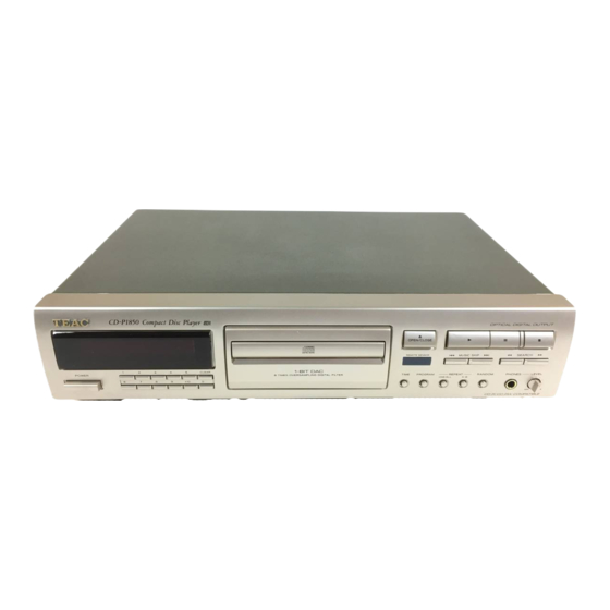
- Page 1 SERVICE MANUAL C C D D - - P P 1 1 8 8 5 5 0 0 COMPACT DISC PLAYER For Europe Effective : February, 2002 S-0050A...
-
Page 2: Table Of Contents
1 SPECIFICATIONS CONTENTS CD PLAYER Pickup: 1 SPECIFICATIONS ・ ・ ・ ・ ・ ・ ・ ・ ・ ・ ・ ・ ・ ・ ・ ・ ・ ・ ・ ・ ・ ・ ・ ・ ・ ・ ・ ・ ・ ・ ・ ・ ・ ・ ・ ・ ・ ・ ・ ・ ・ 3-beam, semiconductor laser 2 EXPLODED VIEWS AND PARTS LIST ・... -
Page 3: Exploded Views And Parts List
2 EXPLODED VIEWS AND PARTS LIST EXPLODED VIEW-1 −3−... - Page 4 EXPLODED VIEW-1 REF.NO. PARTS NO. DESCRIPTION REMARKS 31-00 9A09092400 MECHA,CD93F8NDT 45-01 9A08891700 PCB ASSY,DISPLAY 45-02 9A07273210 PCB ASSY,H.P. 45-03 9A08891810 PCB ASSY,POWER 230V [UK] 9A08891820 PCB ASSY,POWER 230V [E] 45-04 9A08891900 PCB ASSY,MAIN 45-05 9A08892200 PCB ASSY,KEYSW £ 9A07258200 48-09 POWER CORD [UK] £...
- Page 5 EXPLODED VIEW-2 −5−...
- Page 6 EXPLODED VIEW-2 (CD93F8NDT) REF.NO. PARTS NO. DESCRIPTION REMARKS 9A07071300 SWITCH PCB ASSY 9A07072300 CHASSIS,FRAME 9A07071400 PLATE,MAGNET 9A07071500 LEFT RAIL ASSY 9A07071600 RAIL,RIGHT 9A07071800 SUPPORT,MAGNET 9A08438700 CUSHION,RUBBER 9A08438800 CUSHION,RUBBER 9A07072100 HOLDER,MAGNET 9A07072200 SHEET 9A07072400 GEAR,LOADING 9A07072500 GEAR,LIFTER 9A07072600 GEAR,IDLER A 9A07072700 GEAR,IDLER B 9A07072800 PULLEY,MOTOR...
-
Page 7: Pc Boards And Parts List
3 PC BOARDS AND PARTS LIST MAIN PCB −7−... - Page 8 DISPLAY PCB KEYSW PCB −8−...
- Page 9 HP PCB POWER PCB −9−...
- Page 10 MAIN PCB ASSY KEYSW PCB ASSY REF.NO. PARTS NO. DESCRIPTION REF.NO. PARTS NO. DESCRIPTION 9A08891900 PCB ASSY,MAIN 9A08892200 PCB ASSY,KEYSW 9A08894300 PCB,MAIN 9A08900600 PCB,KEYSW £ 9A08899400 C130 C,ELECT 4700U/25V M CN303 9A08893700 PLUG,13P PH H CN101 9A08899700 PLUG,5P PH V SW313,314 9A08467800 SWITCH,TACT...
-
Page 11: Included Accessories
4 INCLUDED ACCESSORIES INCLUDED ACCESSORIES REF.NO. PARTS NO. DESCRIPTION REMARKS 9A08751800 OWNER'S MNL,MULTI [E,UK] 9A08468900 REMOCON 9A07089700 BATTERY 9A06849900 PLUG,CORD,RCA −11−... -
Page 12: Block Diagram
5 BLOCK DIAGRAM MAIN Circuit MECHA ASP&DSP DF+DAC DA11T3CN UPD63711 PCM1710 DRIVER H.P. OUT (Dif Amp) BA5813FM NJM2068D OP/CL MICOM RCA OUT UPD789026 DAC Circuit POWER Circuit POWER DC DIGI OUT POWER AC DISPLAY Circuit DISPLAY DRIVER IR.REM UPD16312 25 KEY −12−... - Page 13 CD-P1850 SCHEMATIC DIAGRAM MAIN PCB, HEADPHONE PCB, MECHA MECHA CD93F8NDT MAIN PCB HEAD PHONE PCB S02 OP/CL CN101 R403 100K CL SW C401 IC401A OP SW 10/16 C403 CN104 R401 0 NJM4556 PH11 220/16 R133 R409 33 R134 P401 7.5K...
- Page 14 CD-P1850 SCHEMATIC DIAGRAM MAIN PCB (DAC Circuit) MAIN PCB (DAC Circuit) IC502B NJM2068-2 R513 C515 R505 R507 JK501A 6.8K 3.9K 10/16 RCA (L) C525 R511 R515 C519 330P 10/16 R521 Q501 Q503 R509 C504 C505 C517 C527 2700P 100P C502...
- Page 15 CD-P1850 SCHEMATIC DIAGRAM DISPLAY PCB, KEY SW PCB DISPLAY PCB NOTES: 1. Resistor values are in ohms (k=kilo-ohms, M=megohms). 2. Capacitor values are in microfarads (p=picofarads). 3. £Parts marked with this sign are safety critical components. They must always be replaced with identical components-refer to the appropriate parts list and ensure exact replacement.
- Page 16 CD-P1850 SCHEMATIC DIAGRAM POWER PCB SW201 T201 SW-POWER J201 LIVE 100V POWERCORD EC202 C201 CONNECTOR 5P ASSY CN201 EC-TERMINAL J202 0.01uF TO PCB MAIN CN105 NEUTRAL EC201 EC-TERMINAL 4L50005800 POWER PCB NOTES: 注 意 C C D D - - P P 1 1 8 8 5 5 0 0 1.
Need help?
Do you have a question about the CD-P1850 and is the answer not in the manual?
Questions and answers