Advertisement
CONTENTS
SAFETY INSTRUCTIONS
・ ・ ・ ・ ・ ・ ・ ・ ・ ・ ・ ・ ・ ・ ・ ・ ・ ・ ・ ・ ・ ・ ・ ・ ・ ・ ・ ・ ・ ・ ・ ・ ・
SPECIFICATIONS
・ ・ ・ ・ ・ ・ ・ ・ ・ ・ ・ ・ ・ ・ ・ ・ ・ ・ ・ ・ ・ ・ ・ ・ ・ ・ ・ ・ ・ ・ ・ ・ ・ ・ ・ ・ ・ ・ ・ ・ ・
MEASUREMENTS AND ADJUSTMENTS
FIP DISPLAY
・ ・ ・ ・ ・ ・ ・ ・ ・ ・ ・ ・ ・ ・ ・ ・ ・ ・ ・ ・ ・ ・ ・ ・ ・ ・ ・ ・ ・ ・ ・ ・ ・ ・ ・ ・ ・ ・ ・ ・ ・ ・ ・ ・ ・ ・ ・
DISPLAY PIN CONNECTION
IC BLOCK DIAGRAMS AND PIN FUNCTIONS
EXPLODED VIEWS AND PARTS LIST
PC BOARDS AND PARTS LIST
INCLUDED ACCESSORIES
NOTES
PC boards shown are viewed from parts side.
●
The parts with no reference number or no parts number in the
●
exploded views are not supplied.
As regards the resistors and capacitors, refer to the circuit diagrams
●
contained in this manual.
Parts marked with this sign are safety critical components. They
£
●
must be replaced with identical components - refer to the appropriate
parts list and ensure exact replacement.
Parts of [ ] mark can be used only with the version designated.
●
[J]:JAPAN [US]:U.S.A. [C]:CANADA
Effective : January, 2002
A A G G - - D D 8 8 9 9 0 0 0 0
・ ・ ・ ・ ・ ・ ・ ・ ・ ・ ・ ・ ・ ・ ・ ・
・ ・ ・ ・ ・ ・ ・ ・ ・ ・ ・ ・ ・ ・ ・ ・ ・ ・ ・ ・ ・ ・ ・ ・ ・ ・ ・ ・ ・
10
・ ・ ・ ・ ・ ・ ・ ・ ・
22
・ ・ ・ ・ ・ ・ ・ ・ ・ ・ ・ ・ ・ ・ ・ ・ ・ ・
24
・ ・ ・ ・ ・ ・ ・ ・ ・ ・ ・ ・ ・ ・ ・ ・ ・ ・ ・ ・ ・ ・ ・ ・ ・
29
・ ・ ・ ・ ・ ・ ・ ・ ・ ・ ・ ・ ・ ・ ・ ・ ・ ・ ・ ・ ・ ・ ・ ・ ・ ・ ・ ・ ・
SERVICE MANUAL
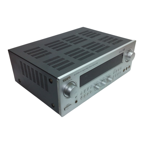
AV Digital Surround Receiver
目 次
2
SAFETY INSTRUCTIONS
3
仕様
・ ・ ・ ・ ・ ・ ・ ・ ・ ・ ・ ・ ・ ・ ・ ・ ・ ・ ・ ・ ・ ・ ・ ・ ・ ・ ・ ・ ・ ・ ・ ・ ・ ・ ・ ・ ・ ・ ・ ・ ・ ・ ・ ・ ・ ・ ・ ・ ・ ・ ・ ・ ・ ・ ・ ・ ・
5
測定と調整
・ ・ ・ ・ ・ ・ ・ ・ ・ ・ ・ ・ ・ ・ ・ ・ ・ ・ ・ ・ ・ ・ ・ ・ ・ ・ ・ ・ ・ ・ ・ ・ ・ ・ ・ ・ ・ ・ ・ ・ ・ ・ ・ ・ ・ ・ ・ ・ ・ ・
8
FIPディスプレイ
・ ・ ・ ・ ・ ・ ・ ・ ・ ・ ・ ・ ・ ・ ・ ・ ・ ・ ・ ・ ・ ・ ・ ・ ・ ・ ・ ・ ・ ・ ・ ・ ・ ・ ・ ・ ・ ・ ・ ・ ・ ・ ・ ・ ・
9
ディスプレイピン接続
ICブロック図とピン機能
分解図とパーツリスト
基板図とパーツリスト
付属品
・ ・ ・ ・ ・ ・ ・ ・ ・ ・ ・ ・ ・ ・ ・ ・ ・ ・ ・ ・ ・ ・ ・ ・ ・ ・ ・ ・ ・ ・ ・ ・ ・ ・ ・ ・ ・ ・ ・ ・ ・ ・ ・ ・ ・ ・ ・ ・ ・ ・ ・ ・ ・
プリント基板図は部品面を示しています。
●
分解図に部番のない部品および品番のない部品は供給できま
●
せん。
標準の抵抗、コンデンサーは省略してあります。
●
回路図を参照してください。
£印は安全重要部品です。
●
交換する時は必ず指定の部品を使用してください。
仕向先
●
[J]:JAPAN [US]:U.S.A. [C]:CANADA
・ ・ ・ ・ ・ ・ ・ ・ ・ ・ ・ ・ ・ ・ ・ ・ ・ ・ ・ ・ ・ ・ ・ ・ ・ ・ ・ ・ ・ ・ ・ ・ ・ ・
・ ・ ・ ・ ・ ・ ・ ・ ・ ・ ・ ・ ・ ・ ・ ・ ・ ・ ・ ・ ・ ・ ・ ・ ・ ・ ・ ・ ・ ・ ・ ・ ・ ・ ・ ・ ・ ・ ・ ・
・ ・ ・ ・ ・ ・ ・ ・ ・ ・ ・ ・ ・ ・ ・ ・ ・ ・ ・ ・ ・ ・ ・ ・ ・ ・ ・ ・ ・ ・ ・ ・ ・ ・ ・ ・
・ ・ ・ ・ ・ ・ ・ ・ ・ ・ ・ ・ ・ ・ ・ ・ ・ ・ ・ ・ ・ ・ ・ ・ ・ ・ ・ ・ ・ ・ ・ ・ ・ ・ ・ ・ ・ ・
・ ・ ・ ・ ・ ・ ・ ・ ・ ・ ・ ・ ・ ・ ・ ・ ・ ・ ・ ・ ・ ・ ・ ・ ・ ・ ・ ・ ・ ・ ・ ・ ・ ・ ・ ・ ・ ・
注 意
2
4
5
8
9
10
22
24
29
S-0000A
Advertisement
Table of Contents

Related Manuals for Teac AG-D8900


Summary of Contents for Teac AG-D8900
- Page 1 SERVICE MANUAL A A G G - - D D 8 8 9 9 0 0 0 0 AV Digital Surround Receiver CONTENTS 目 次 SAFETY INSTRUCTIONS SAFETY INSTRUCTIONS ・ ・ ・ ・ ・ ・ ・ ・ ・ ・ ・ ・ ・ ・ ・ ・ ・ ・ ・ ・ ・ ・ ・ ・ ・ ・ ・ ・ ・ ・ ・ ・ ・ ・...
-
Page 2: Safety Instructions
SAFETY INSTRUCTIONS PRECAUTIONS DURING SERVICING The leakage-current should be less than 0.5mA rms AC. The resistance measurement should be done between 1. Parts identifide by the ( )symbol parts are critical accessible exposed metal parts and power cord plug for safety. Replace only with parts number specified. prongs with the power switch (if included) "ON". -
Page 3: Specifications
SPECIFICATIONS Amplifier Section AM Tuner Section Surround Output Power (0.9 % THD, 1 kHz, 8 ohms): Tuning Range: 100 + 100 watts (Front) 522 kHz – 1,620 kHz (10 kHz steps) 100 watts (Center) 539 kHz – 1,720 kHz (10 kHz steps: [us/c] ) 100 + 100 watts (Rear) Usable Sensitivity: 55 dB/m Delay Time:... - Page 4 仕 様 ■アンプ部 ■AMチューナー部 サラウンド出力 (0.9% THD, 1kHz, 6Ω) 受信周波数 ...... 522kHz∼1,620kHz (9kHzステップ) フロント ............100W+100W 感度 ..................55dB/m センター ................100W 高調波歪み率 ............0.8% (85dB/m) リア ..............100W+100W S/N比 ..............45dB (85dB/m) ディレイタイム ドルビーデジタル........リア:0∼15ms ■ビデオ部 センター:0∼5ms 入力感度/インピーダンス ........1.0Vp-p/75Ω ドルビープロロジック ......リア:15∼30ms 出力レベル/インピーダンス ........1.0Vp-p/75Ω 周波数特性......* ライン:20Hz∼65kHz, +1/−3dB SN比...
-
Page 5: Measurements And Adjustments
MEASUREMENTS AND ADJUSTMENTS ALIGNMENT INSTRUCTIONS EQUIPMENT NEEDED: AM Signal Generator FM Signal Generator Oscilloscope VTVM(AC, DC) Test loop antenna (AM Adjustment) Dummy antenna (FM Adjustment) Distortion analyser IMPORTANT 1. Check power-source voltage. 2. Set the function switch to band aligned. 3. - Page 6 1. TUNING FREQUENCY RANGE ADJUSTMENTS (FM) DC VOLTMETER ....CONNECT TO TEST POINT J208 and GND Band Frequency Adjust for Adjustment 87.50MHz 1.6V [76.00MHz] [1.6V] [L7] 530 kHz L105 J208 [US/C] [530 kHz] [1V] [L105] 2. AM TRACKING ADJUSTMENT Signal Generator ......Connects to the AM ANT. Coil through the loop antenna. Adjust for the indication of VTVM of the wave form of scope to be maximum.
- Page 7 4. FM MONO DISTORTION ADJUSTMENT DC VOLT METER ......Connect to J205 (-), J207 (+) through the chock coil (100uH). Signal Generator ......Connect to FM ANT Jack (FM IN) through the dummy. Distortion Meter ......Connect to the output. Frequency Adjust for Adjustment 100.10MHz T101...
-
Page 8: Fip Display
FIP DISPLAY ANODE CONNECTION SOURCE VCR 1 CHURCH DISCO STADIUM HALL THEATER AC-3 DELAY.T STEREO PRESET CH. MEMO TAPE DIGITAL PRO LOGIC TUNED STEREO... - Page 9 PIN CONNECTION Pin No. Connection P16 P15 Pin No. Connection Pin No. Connection 10G NP Pin No. Connection...
- Page 10 IC PIN FUNCTION (u-COM : ANAM1308AT,O.T.P :TMP87PM78F) : IC71 PIN No. SYMBOL DESCRIPTION 1,25 Power Supply Port(+5V) Function SW1,SW2 Function Encoder Control Port Speaker ON/OFF Front Speaker Relay Drive Port(“H”) Not Use(No connection) DSP Reset Reset (Initial Clear) Port for YSS912 Surr.
- Page 12 Dolby Digital/Pro Logic DTS DECODER (YSS912C:INPUT IC43) PIN No. SYMBOL DESCRIPTION 1,31,71 VDD1 +5V Power Supply(for I/Os) RAMCEN External SRAM interface /CE RAMA16 External SRAM interface address 16 RAMA15 External SRAM interface address 15 SDIB0 PCM input 0 to Sub DSP(not use) SDIB1 PCM input 1 to Sub DSP(not use) SDIB2...
- Page 13 PIN No. SYMBOL DESCRIPTION RAMA2 External SRAM interface address 2 72 ~ 79 RAMD0~7 I+/O External SRAM interface data (STREAM0~7 output when External SRAM is not in use) SDWCK0 Word clock input for SDIA, SDOA, SDIB, SDOB SDBCK0 Bit clock input for SDIA,SDOA,SDIB,SDOB SDIA0 AC-3 Bitstream (or PCM) data input for Main DSP SDIA1...
- Page 14 YSS912C BLOCK DIAGRAM SDOB Interface /CSB 24 * 16 OVFB Sub DSP RAMA 0~16 RAMOEN RAMWEN RAMCEN SDIB Interface RAMA 0~7 SDIBSEL SDIB3 SDIB2 SDIB1 SDIB0 SDOA2 SDOA1 SDOA0 SDOA Interface 24 * 16 Main DSP OPORT 0~7 AC-3/Pro Logic/DTS decoder Input Buffer IPORT 0~7...
- Page 15 M62446FP (ELECTRONIC VOLUME/INPUT IC31) OUT4 DVoo OUT3 OUTPUT volume PORT MCU I/F OUT2 DATA OUT1 LATCH AVoo DGND volume SWin AGND GNDS SWout volume SRin SRout SLin SLout GNDC Cout volume Rout GNDR Lout AVss volume GNDL BYPASSR volume BYPASSL LTRE RTRE tone...
- Page 16 PIN ASSIGNMENT (74HCU04AFN : IC40 ) LOGIC SYMBOL (10) (11) (13) (12) TRUTH TABLE...
- Page 17 AK4112AVF (DIR/INPUT IC41) AVSS AVDD MCKO1 MCKO2 Clock Clock X’tal Recovery Generator Oscillator Input Selector 96kHz FS96 Detect DAUX LRCK BICK Audio V/TX DAIF SDTO Decoder DVDD DVSS TVDD System CCLK CDTO Control AC-3/MPEG Error Detect CDTI Detect AUTO P/S="L" [Serial Control Mode] AVSS AVDD...
- Page 18 LC72131 (PLL SYNTHESIZER/ TUNER IC11) REFERENCE PHASE DETECTOR DIVIDER CHARGE PUMP XOUT SAMLLOM COUNTER UNLOCK FMIN 1/16, 1/17 4bits AOUT DETECTOR 12bits PROGRAMMABLE AMIN DIVIDER UNIVERSAL DATA SHIFT REGISTER IFIN LATCH COUNTER POWER RESET BO1 BO2 BO3 BO4 LA1837 (MPX + IF / TUNER IC12) 3 rd 5 th DECODER ANTI-BIRDIE...
- Page 19 KIC9164AF (FUNCTION/INPUT IC20) BLOCK DIAGRAM L-COM R-COM L-COM R-COM L-COM R-COM L-COM R-COM DATA SHIFT REGISTER KIC9163AF (FUNCTION/INPUT IC21) BLOCK DIAGRAM L-COM R-COM L-COM R-COM L-COM R-COM L-COM R-COM DATA SHIFT REGISTER...
- Page 20 BLOCK DIAGAM (NJM2296M /MAIN IC96) Vin1 Vin2 Vout1 6.2dB dirver Vin3 6.2dB Vout2 dirver Vin4 6.2dB Vout3 dirver Vin5 LA6462M/6458M PIN CONFIGURATION • PIN FUNCITON 1. A OUTPUT 2. A-INPUT 3. A+INPUT 4. V 5. B+INPUT 6. B-INPUT 7. B OUTPUT 8.
- Page 21 TRANSISTOR, REGULATOR IC BLOCK DIAGRAM TO-92S TO-92 TO-220 TO-92L 1. Emitter 1. Emitter 1. Emitter 1. INPUT 2. Collector 2. Collector 2. Collector 2. OUTPUT 3. Base 3. Base 3. Base 3. GND 1 2 3 12 3 KSA1175Y KRC114M KTD1302T KTA1268GR KSA916Y...
- Page 22 EXPLODED VIEW (AG-D8900T/C) DESCRIPION PARTS-No. Q,ty FRONT PANEL K(C)GW1A279ZH10 BADGE KGB1A056H12 STANDBY KNOB KBT2A450 SPEAKER KNOB K(C)BT1A715 MODE KNOB K(C)BT1A716 PHONES PCB ASS'Y PCB BRACKET KMK1A010 FRONT PCB ASS'Y JACK PCB ASS'Y VOLUME PCB ASS'Y KGX1A293Z LED SHEET S-VIDEO PCB ASS'Y LED SHEET(3P) KGX1A243X WASHER...
-
Page 23: Exploded View
EXPLODED VIEW REF.NO. PARTS NO. DESCRIPTION REMARKS 9A08886700 PANEL,FRONT [J] 9A08956000 PANEL,FRONT [US,C] 9A08887100 BADGE 9A08886600 KNOB,STANDBY [J] 9A06777500 KNOB,POWER [US,C] 9A08886400 KNOB,SPEAKER [J] 9A08955800 KNOB,SPEAKER [US,C] 9A08886500 KNOB,MODE [J] 9A08955900 KNOB,MODE [US,C] ---------- PHONES PCB ASSY 9A08886900 BRACKET,PCB 9A08887000 FRONT PCB ASSY [J] 9A08887010 FRONT PCB ASSY [US,C]... - Page 27 INPUT PCB ASSY INPUT PCB ASSY REF.NO. PARTS NO. DESCRIPTION REF.NO. PARTS NO. DESCRIPTION 9A08888000 INPUT PCB ASSY [J] VR11 9A08040600 R,SEMI-FIXED 10K OHM 9A08888010 INPUT PCB ASSY [US,C] VR12 9A08040700 R,SEMI-FIXED 22K OHM 9A08953300 PCB,INPUT VR13 9A08040600 R,SEMI-FIXED 10K OHM 9A08215300 PACK,FRONT END [US,C] X101...
- Page 28 MAIN PCB ASSY MAIN PCB ASSY REF.NO. PARTS NO. DESCRIPTION REF.NO. PARTS NO. DESCRIPTION £ 9A08946400 9A08887900 MAIN PCB ASSY [J] Q656 TR,KTD2061Y £ 9A08952600 9A08887910 MAIN PCB ASSY [US,C] Q657-Q660 TR,2SC4468 £ 9A08952700 9A08950900 PCB,MAIN Q661-Q665 TR,2SA1695 £ 9A08952600 9A08952200 HEAT SINK Q670...
-
Page 29: Included Accessories
INCLUDED ACCESSORIES REF.NO. PARTS NO. DESCRIPTION REMARKS 9A08523201 OWNER'S MNL,E/F [US,C] 9A08523300 OWNER'S MNL,J [J] 9A08763300 REMOTE CONTROL UNIT,UR-417 9A08886200 BATTERY [J] 9A08886000 ANT,FM T 9A08886100 AM LOOP ANTENNA ASSY... -
Page 30: Notes
AG-D8900 SCHEMATIC DIAGRAM NOTES: 1. Resistor values are in ohms (k=kilo-ohms, M=megohms). 2. Capacitor values are in microfarads (p=picofarads). 3. £Parts marked with this sign are safety critical components. They must always be replaced with identical components-refer to the appropriate parts list and ensure exact replacement. -
Page 31: Notes
AG-D8900 SCHEMATIC DIAGRAM NOTES: 1. Resistor values are in ohms (k=kilo-ohms, M=megohms). 2. Capacitor values are in microfarads (p=picofarads). 3. £Parts marked with this sign are safety critical components. They must always be replaced with identical components-refer to the appropriate parts list and ensure exact replacement. -
Page 32: Notes
AG-D8900 SCHEMATIC DIAGRAM A A G G - - D D 8 8 9 9 0 0 0 0 NOTES: 注 意 INSTRUCTIONS FOR SERVICE PERSONNEL 1. 抵抗の単位はΩ (k=kΩ,M=MΩ) です。 1. Resistor values are in ohms (k=kilo-ohms, M=megohms). BEFORE RETURNING APPLIANCE TO THE CUSTOMER, MAKE LEAKAGE- 2.
Need help?
Do you have a question about the AG-D8900 and is the answer not in the manual?
Questions and answers