Samsung YP-R1 Service Manual
Hide thumbs
Also See for YP-R1:
- User manual (104 pages) ,
- User manual (95 pages) ,
- User manual (95 pages)
Table of Contents

Related Manuals for Samsung YP-R1


Summary of Contents for Samsung YP-R1
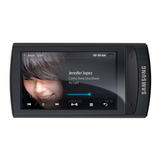
- Page 1 MP3 Player Model Name : YP-R1 Model Code : YP-R1AB/XER SERVICE Manual MP3 Player CONTENTS 1. Precaution 2. Product Specification 3. Disassembly & Reassembly 4. Troubleshooting 5. Exploded View & Part List 6. PCB Diagram 7. Schematic Diagram YP-R1...
- Page 2 Asia asia.samsungportal.com Mideast & Africa mea.samsungportal.com © Samsung Electronics Co.,Ltd. Oct. 2009 This Service Manual is a property of Samsung Electronics Printed in Korea Co.,Ltd. Any unauthorized use of Manual can be punished under applicable International and/or domestic law.
-
Page 3: Table Of Contents
Contents 1. Precaution 1-1 Safety Precautions ................... 1-1 1-2 Static Electricity Precautions ................1-2 2. Product Specification 2-1 Product Feature ....................2-1 2-2 Specifications ....................2-2 2-3 Specifications Analysis ..................2-4 2-4 Accessories ......................2-6 3. Disassembly & Reassembly 3-1 Overall Disassembly & Reassembly ..............3-1 4. -
Page 4: Precaution
3. You should not use this product near or in water. 4. You should only use the power supply provided by the company. 5. If replacement material is required you should only use standardized materials, if you use non-standardized materials you could cause failure to the product. Samsung Electronics... -
Page 5: Static Electricity Precautions
9. Minimize body motions when handing unpackaged replacement ESDs. Motions such as brushing clothes together, or lifting a foot from a carpeted floor can generate enough static electricity to damage an ESD. Samsung Electronics... -
Page 6: Product Specification
Video playback without converting - Playback is possible by simply transferring files without converting. All file formats to the right are supported. Compact design - Compact design giving excellent portability. 45.5(H) x 85.2(V) x 8.9(D) mm Samsung Electronics... -
Page 7: Specifications
90dB with 20kHz LPF (based on 1kHz 0dB) Supported Number of File: Max. 5000 Files/Folders Folder: Max. 5000 (including File) Music: 25 hours (MP3 128 kbps, Volume level 15, Normal sound mode, LCD off) Playing Time Video: 5 hours (Brightness 3, Volume level 15, Normal sound mode, SVI) Samsung Electronics... - Page 8 FM Useable 38dBμ Sensitivity Wireless System Bluetooth QD ID B015440 Emission Type RF power CLASS I Transmit Frequency 2402MHz ~ 2480MHz Receive Frequency 2402MHz ~ 2480MHz Number of channels 79 channels Modulation System GFSK Communication Mode Semi-duplex Operation Humidity 0 ~ 95% Specifications Version 2.0 + EDR Supported Module BCM2070 Samsung Electronics...
-
Page 9: Specifications Analysis
Product Specification 2-3 Specifications Analysis Model YP-R1 YP-Q2 Photo Storage Type Flash memory (MLC) Flash memory (MLC) SIZE: 2.6" WQVGA Display Color: 16.7M LCD SIZE: 2.4" QVGA TFT LCD Display (Dot pitch: 0.14475 (H) x 0.14475 (V)) Resolution: 320 (H) x 240 (V) - Page 10 Product Specification Model YP-R1 YP-Q2 Photo DNSE 3.0 DNSE 3.0 DNSE (General, Studio, Rock, Classic, Jazz, Ballad, (General, Studio, Rock, Classic, Jazz, Ballad, Club, R&B, Dance, Cafe, Concert, Cathedral) R&B, Dance, Concert) User EQ (9 band control) (9 band control) Street Mode ...
-
Page 11: Accessories
Product Specification 2-4 Accessories 2-4-1 Supplied Accessories Accessories Item Item Code Remark Earphones GM59-01016A Samsung Service GM39-01002A USB Cable Center User's Manual GM68-01002J Samsung Electronics... -
Page 12: Disassembly & Reassembly
1) Remove the two screws using a phillips screwdriver, and remove the SUS BRACKET. 1) Disconnect the case from the main body by pulling the AL CASE down. 1) Remove the screw from the MAIN PCB. Samsung Electronics... - Page 13 1) Insert a flat screwdriver or tweezers into the hole next to the battery FPCB and remove the battery FPCB. 1) Remove the battery that is fixed with double sided tape onto the LCD MODULE . Ensure that the battery doesn’t get damaged. Samsung Electronics...
- Page 14 Disassembly & Reassembly Description Description Photo 1) When removing the hooked LCD, pull the bottom of the LCD (2) upwards while widening the side of the Touch Assy (1). 1) After disassembly Samsung Electronics...
- Page 15 MEMO Samsung Electronics...
-
Page 16: Troubleshooting
Fig. 4-1. Check CPU_RST - HIGH Check that the clock on X403 and R406 - LOW X402 oscillates. See the waveform and See the waveform and the image in Fig. 4-2. the image in Fig. 4-3. Faulty Samsung Electronics... - Page 17 Troubleshooting Check the voltage on the battery. Replace the battery and check the Complete voltage again. Samsung Electronics...
- Page 18 P_3.0V VREFIN FASTR_DIG VREOUT COMP VDD_FUSE 100nF C302 MAIN CPU-1, page 7-2 U401 U701 U102 U301 U101 MAIN PCB Top, page 6-1 MAIN PCB Bottom, page 6-3 C316 C318 C303 U402 U801 CON801 <Fig. 4-1> Samsung Electronics...
- Page 19 NAND_R/B5 U402 S-35392A CSPI1_MISO/GPIO3_1 NAND_R/B6 UART3_RXD_MUX/GPIO2_14 CSPI1_MOSI/GPIO3_0 UART3_TXD_MUX/GPIO2_15 UART3_R_RTS/GPIO2_16 1 32KO UART3_CTS/GPIO2_17 PER6 2 XOUT I2C_DAT0 GPIO2_18 I2C_CLK0 GPIO2_19 3 XIN U402 AUD_DAO U801 4 VSS INT2 AUD_DAI AUD_BCLK AUD_LRCK MAIN PCB Top, page 6-1 <Fig. 4-2> Samsung Electronics...
- Page 20 CSPI1_MISO/GPIO3_1 NAND_R/B6 C402 U101 CSPI1_MOSI/GPIO3_0 1 32KO X402 32.768KHz 2 XOUT I2C_DAT0 I2C_CLK0 3 XIN 4 VSS INT2 U401 C403 U402 U801 U701 MAIN PCB Bottom, page 6-3 MAIN PCB Top, page 6-1 <Fig. 4-3> U101 Samsung Electronics...
- Page 21 Is audio signal present? Does U701 work? Replace U701. Replace the board. (Detailed inspection is required.) Does U301 work? Replace U301. Is R711 high? See the waveform and the image in Fig. 4-4. Replace the board. (Detailed inspection is required.) Samsung Electronics...
- Page 22 U504 LOUT_EP R713 MUTE C722 D2_2 1 S1 2.5V 330uF ROUT_EP 2 G1 D1_2 D1_1 3 D2_1 4 S2 U401 U702 FDMA1028NZ U701 AUDIO CODEC, page 7-6 U101 U801 MAIN PCB Top, page 6-1 <Fig. 4-4> Samsung Electronics...
- Page 23 Disassemble the main body and check if the TOUCH FPCB is connected Does the touch pad respond? correctly or faulty. If the touch pad is faulty, replace it. Replace the board. Does the touch pad have a defect? (Detailed inspection is required.) Samsung Electronics...
- Page 24 Does U701 work? Replace U701. Replace the board. (Detailed inspection is required.) Is the 32.768 clock displayed? Does X402 work? Replace X402. (R118) See the waveform and the image in Fig. 4-5. Replace the board. (Detailed inspection is required.) Samsung Electronics...
- Page 25 PCM_IN PCM_OUT PCM_CLK U101 PCM_SYNC C112/C124 Should be placed COEX_IN COEX_OUT0 close to VDDPX(G1)/VDDIF(B1)PIN. COEX_OUT1 C113 Should be placed close to VDDLNA(E1)PIN. C116 Should be placed close to VDDTF(C1)PIN. MAIN PCB Top, page 6-1 <Fig. 4-5> 4-10 Samsung Electronics...
- Page 26 Disassemble the main body and Are the LED_PWM and LED_DIMMING replace the LCD. ports’ voltages high? See the waveform and the image in Fig. 4-6. Replace the board. (Detailed inspection is required.) Samsung Electronics 4-11...
- Page 27 INN_BATT LOW : 0.82V R631 U604 MAX17040G+T RESET_IN P_3.0V 100K R633 RESET_SW I2C_DAT1 1 CTG R628 U401 I2C_CLK1 2 CELL 100K R632 3 VDD 4 GND U701 MAIN PCB Top, page 6-1 CON601 <Fig. 4-6> 4-12 Samsung Electronics U101...
- Page 28 Check voltage of the battery. Replace the board. R621 – High while charging, (Detailed inspection is required.) R618 – Low while charging and High when fully charged. See the waveform and the image in Fig. 4-8. Change the battery Samsung Electronics 4-13...
- Page 29 U604 UART_RX1 UART_TX1 3.9ohm R810 USB_D+ LINE_OUT_R LINE_OUT_L U504 PBA_CE INN_BATT U801 NCP360SNT1G USB_P5V U401 5 OUT 4 FLAG U701 24PIN IO INTERFACE, page 7-7 U101 U402 U801 MAIN PCB Top, page 6-1 <Fig. 4-7> 4-14 Samsung Electronics...
- Page 30 HIGH : 1.05V LOW : 0.82V R631 U604 MAX17040G+T RESET_IN 100K R633 RESET_SW I2C_DAT1 1 CTG R628 I2C_CLK1 2 CELL 100K U601 R632 3 VDD 4 GND MAIN PCB Bottom, page 6-3 U501 <Fig. 4-8> U301 Samsung Electronics 4-15...
- Page 31 Replace the MIC. when checking visually? Disassemble the main body and Is the bias voltage present? replace the MIC. (R704 - 1.5V) See the waveform and the image in Fig. 4-9. Replace the board. (Detailed inspection is required.) 4-16 Samsung Electronics...
- Page 32 P_3.0V AUDIO CODEC, page 7-6 U401 U701 P_3.0V AB 1000 R706 R705 200K L702 EARPHONE_DET AB 1000 R710 J701 U101 L703 R719 L704 VIDEO_OUT 600ohm FM_ANT U402 U801 MAIN PCB Top, page 6-1 <Fig. 4-9> Samsung Electronics 4-17...
- Page 33 (U704 Pin 6) Replace the board. See the waveform and (Detailed inspection is the image in Fig. 4-10. required.) Is output present? Is it DRM content? Replace the content. Replace the board. (Detailed inspection is required.) 4-18 Samsung Electronics...
- Page 34 AUDIO CODEC, page 7-6 C721 2.5V 330uF LOUT_EP U501 R713 MUTE U102 U301 C722 D2_2 1 S1 2.5V 330uF ROUT_EP 2 G1 D1_2 D1_1 3 D2_1 4 S2 U702 FDMA1028NZ MAIN PCB Bottom, page 6-3 CON801 <Fig. 4-10> Samsung Electronics 4-19...
- Page 35 See the waveform and (Detailed inspection is the image in Fig. 4-11. required.) Does U102 work? Replace U102. Is 1.2V present? (B101) See the waveform and the image in Fig. 4-11. Replace the board. (Detailed inspection is required.) 4-20 Samsung Electronics...
- Page 36 VDDLNA(E1)PIN. PCM_IN AUD_DATA_IN PCM_OUT AUD_DATA_OUT PCM_CLK C116 Should be placed AUD_BCLK PCM_SYNC AUD_LRCK close to VDDTF(C1)PIN. COEX_IN COEX_OUT0 COEX_OUT1 C116 Should close to VDD U501 U102 U301 MAIN PCB Bottom, page 6-3 <Fig. 4-11> CON801 Samsung Electronics 4-21...
- Page 37 Upgrade Tool and present in the device “My Computer”? check if it works. manger? Install a driver and check it again. Can you format Can you access? on the browser? Replace the Board Complete 4-22 Samsung Electronics...
-
Page 38: Upgrade Methods
Files for upgrading main firmware YP-R1 → R1.rom Files for upgrading TOUCH firmware YP-R1 → touch_fw.bin How to main firmware upgrade. A. You can upgrade firmware copying R1.rom on the YP-R1’s file directory. B. You can upgrade firmware using R1 Update Tool. - You will use B-way if A-way make trouble. - Page 39 Troubleshooting 4-2-1 Copy R1.rom (A-1) 1. Copy the R1.rom on the YP-R1’s file directory. 2. Paste the “R1.rom” to the root director of the YP-R1. 4-2-2 Reboot YP-R1 (A-2) 1. You can see “Firmware Update” on the screen and then menu will come into being on the screen after upgrading.
- Page 40 Troubleshooting 4-2-3 Install Driver (B-1) 1. Double click on the file below to execute the driver installation. → windriver/wd_install_4NT.bat If driver is already installed you do not need to reinstall. Samsung Electronics 4-25...
- Page 41 If vc_s1_redist_x86.exe makes error like this, use another way to install. Install 1) vc_s1_redist_x86.exe file to C:\ root directory. 2) Click “Start” → Click “Run(R)” → Input “cmd” → [Enter or Click OK] 3) Input next command at DOS window. cd c:\ [Enter] vc_s1_redist_x86.exe /t:c: [Enter] 4-26 Samsung Electronics...
- Page 42 4-2-4 Enter Firmware Upgrade Mode (B-2) 1. SET should be bootstrap mode for upgrading firmware. 2. How to be 1) Connect PC and SET by USB Cable. 2) When you pushing the power button, press the reset button at 5 seconds. Samsung Electronics 4-27...
- Page 43 Troubleshooting 4-2-5 Select Driver (B-3) 1. When pc realized firmware upgrade mode, it calls driver (only first connect) Make folder in the unpacking directory. 4-28 Samsung Electronics...
- Page 44 Troubleshooting Install completed. Check device manager. Samsung Electronics 4-29...
- Page 45 2. Choose the firmware (R1.ROM is in the firmware realease). 3. You can upgrade all if you choose each images that Mboot, Linux, Root File & System file. Skip image (Mboot or Linux or Root File System) if you don’t need to upgrade. 4-30 Samsung Electronics...
- Page 46 Check if you want to erase all data in NAND flash memory. Situation to erase NAND Check if you want to erase - SET doesn’t work. (can’t booting) all data in NAND flash memory. - Install Method of release note needs to Erase. Samsung Electronics 4-31...
- Page 47 Troubleshooting 4-2-7 Copy touch_fw.bin (C-1) 1. Copy touch_fw.bin on the YP-R1’s file directory. 2. Paste the “touch_fw.bin” file to the root directory of the YP-R1. 4-2-8 Reboot YP-R1 (C-2) 1. You can see “Touch Sensor Updating” on the screen and then screen will be off.
- Page 48 MEMO Samsung Electronics 4-33...
-
Page 49: Exploded View & Part List
Exploded View & Part List 5. Exploded View & Part List 5-1 Exploded View QVO03 QME04 QVO01 QFM01 QBD01 QLC01 QBR01 QBA01 QMP01 QJA01 QCP01 QSM09 This Document can not be used without Samsung’s authorization. Samsung Electronics... - Page 50 QJA01 GM63-01030A COVER-JACK;YP-R1,PC,43.8,9,BLACK QLC01 GM96-01009A ELA ETC-YP-R1 LCD ASS’Y;YP-R1,SAMSUNG,LC QME04 AH97-03272B ASSY FRAME-TOUCH;MP3,YP-R1,WINDOW,TSP,KN QMP01 GM92-01022A ASSY PBA MAIN;YP-R1,WORLDWIDE,4GB QSM09 6003-001660 SCREW-TAPTYPE;CH,+,B,M1.4,L3,NI PLT,SWRC QVO01 GM64-01012A KNOB-VOLUME;YP-R1,PC,40.28,7.75,BLACK QVO03 GM64-01013A KNOB-POWER;YP-R1,PC BLACK,BLACK Samsung Electronics This Document can not be used without Samsung’s authorization.
-
Page 51: Electrical Part List
2007-007538 R-CHIP;56Kohm,1%,1/16W,TP,1005 GM68-01002J MANUAL USERS-QSG;YP-R1,XER,RUS/URK, AH69-02524A PACKING-USB;YP-Q1,PPR-OTH,0.6,171,1 2007-007590 R-CHIP;82Kohm,1%,1/16W,TP,1005 AH69-02525A PACKING-IB;YP-Q1,PPR-OTH,0.6,210,21 2007-007592 R-CHIP;270Kohm,1%,1/16W,TP,1005 AH69-02609A PACKING-SET;YP-R1,PAPER,PAPER,0.5,1 2007-007697 R-CHIP;2.4Kohm,1%,1/16W,TP,1005 2007-007942 R-CHIP;1Mohm,1%,1/16W,TP,1005 AH69-02670A PACKING-PAD;YP-R1,PAPER,0.5,50,90,4 2007-008167 R-CHIP;120Kohm,1%,1/16W,TP,1005 GM69-01011B PACKING-CASE;YP-R1,PAPER,PAPER,0.5, AH63-01219M COVER-BAG;YP-PB2,HDPE,0.03,175,240, 2007-008294 R-CHIP;33ohm,1%,1/16W,TP,1005 This Document can not be used without Samsung’s authorization. Samsung Electronics... - Page 52 Q’ty SNA Remark GM59-01010A EAR PHONE OPTION-EARPHONE;YA-EH420, GM68-01014A LABEL-EAR-PHONE;YP-R1,EUROPE,ART,AR 6902-000297 BAG PE;LDPE,T0.05,W80,L140,TRP,4-PE QCP01 AH63-01972A CUSHION-PCB;YP-R1,PORON,1.2mm,30,23 AH68-00511G LABEL-SEAL;YP-Z5F,ART PAPER GM63-01086A SHEET-WINDOW;YP-R1,P E T,0.05,35,50 GM74-01005A TAPE-CONNECTOR;YP-R1,110PE,9.7*17.5 QBA01 4302-001229 BATTERY-POLYMER;3.7V,500mAH,CELL,20 AH68-00508U LABEL SERIAL;COMMON,ELS,90 Samsung Electronics This Document can not be used without Samsung’s authorization.
- Page 53 MEMO Samsung Electronics...
-
Page 54: Pcb Diagram
U401 U701 U101 Description U402 U801 24MHz Crystal - Main CLK Finger GASKET - Improved resistance to ESD 32.768KHz Crystal - Bluetooth CLK FM Tuner IC - Supports reception of FM signals CODEC IC - Supports voice codec Samsung Electronics... - Page 55 PCB Diagram 6-1-1 Test Point Wave Form Samsung Electronics...
-
Page 56: Main Pcb Bottom
Mobile DDR SDRAM IC - Supports data transfer in the system PM IC CON801 - Battery charger and dual buck converter are built in Battery connector - Connects and holds the battery in position Finger GASKET - Improved resistance to ESD Samsung Electronics... - Page 57 LCD_D[7] LED3 UART RX GROUND LCD_D[8] VOUT(LED+)_ UART TX R-CH LCD_D[9] LCD_TP USB D+ L-CH LCD_D[10] USB POWER LCD_D[11] LINE OUT R LCD_D[12] LINE OUT L LCD_D[13] GROUND LCD_D[14] CRADLE_ANT(FM) BATTERY INPUT BATTERY INPUT EXTERNAL BATTERY DETECT PBA_CE Samsung Electronics...
- Page 58 PCB Diagram 6-2-2 Test Point Wave Form Samsung Electronics...
- Page 59 MEMO Samsung Electronics...
-
Page 60: Schematic Diagram
50 ohm CODEC △ AUDIO IIS / IIC Uart RX,TX [WM1808] BLOCK Bluetooth UART (AUDIO/MIC) TV-OUT interface (RTC) FM TUNER (BCM2048B) AUDIO TV-OOUT 32.768KHz (RTC) [3.5φ JACK] 24MHz (MAIN CLK) Samsung Electronics This Document can not be used without Samsung’s authorization. -
Page 61: Main Cpu-1
IOG_BACK DDR_SD_AD[7] DRAM_A7 DDR_SD_AD[8] DRAM_A8 VDD_TVDIG DDR_SD_AD[9] DRAM_A9 P_2.5V IOR_BACK DDR_SD_AD[10] DRAM_A10 NVCC_SRTC_POW DDR_SD_AD[11] DRAM_A11 DDR_SD_AD[12] DRAM_A12 FASTR_ANA RSET P_3.0V DRAM_A13 VREFIN FASTR_DIG DRAM_A14 VREOUT COMP VDD_FUSE 100nF C302 This Document can not be used without Samsung’s authorization. Samsung Electronics... -
Page 62: Main Cpu-2
UART3_CTS/GPIO2_17 MUTE I2C_CLK1 32.768KHz PER6 I2C_DAT1 2 XOUT I2C_DAT0 GPIO2_18 BT_WAKE I2C_CLK0 GPIO2_19 3 XIN BT_RST PWR_IN_CPU AUD_DAO AUD_DATA_OUT 4 VSS INT2 AUD_DAI AUD_DATA_IN AUD_BCLK AUD_BCLK AUD_LRCK AUD_LRCK C403 Samsung Electronics This Document can not be used without Samsung’s authorization. -
Page 63: Memory (Sdram, Nand-Flash)
NC_5 IO7-1 NAND_DQ[7] NAND_CS_CTL NC_6 C517 NAND_CS7 100nF 100nF NC_6 VSS_5 NAND_DQ[0-7] VSS_5 NAND_DQ[0-7] NC_7 P_3.0V NC_7 NC_8 NC_8 NC_9 NC_9 R/B2-2 NAND_R/B3 R/B2-2 NAND_R/B7 NAND_CS3 NAND_CS6 NAND_CS2 NAND_CPU_CS2 This Document can not be used without Samsung’s authorization. Samsung Electronics... -
Page 64: Power Management
LOW : 0.82V R631 U604 MAX17040G+T RESET_IN P_3.0V 100K R633 RESET_SW 1 CTG I2C_DAT1 R628 LP_CTL I2C_CLK1 2 CELL 100K R632 RESET_SW 3 VDD T602 PWR_SW 4 GND CON601 Samsung Electronics This Document can not be used without Samsung’s authorization. -
Page 65: Audio Codec
L702 EARPHONE_DET AB 1000 R710 C722 J701 1 S1 D2_2 330uF 2.5V ROUT_EP L703 2 G1 D1_2 D1_1 3 D2_1 4 S2 R719 L704 U702 VIDEO_OUT FDMA1028NZ 600ohm FM_ANT This Document can not be used without Samsung’s authorization. Samsung Electronics... -
Page 66: 24Pin Io Interface
18: LINE OUT L TOUCH_DAT LINE_OUT_L 19: GND TOUCH_CLK R806 20: JTAG_TMS CON802 21: BATT 22: BATT 23: JTAG_TDI PBA_CE 24: PBA CE INN_BATT U801 NCP360SNT1G USB_P5V 5 OUT 4 FLAG Samsung Electronics This Document can not be used without Samsung’s authorization. -
Page 67: Pba / Lcd Interface
L IN LCD_RED1 LCD_RED2 R IN LCD_RED3 LCD_RED4 FM_ANT FM ANT LCD_RED5 LCD_RED6 LCD_RED7 PCB OUT-SIDE LED_PWM LED- LED+ Contact with LCD-SUS LCD GUIDE HOLE SYMBOL SCREW HOLE SYMBOL This Document can not be used without Samsung’s authorization. Samsung Electronics... -
Page 68: Bluetooth / Fm
AUD_DATA_OUT PCM_CLK AUD_BCLK PCM_SYNC AUD_LRCK C112/C124 Should be placed COEX_IN COEX_OUT0 close to VDDPX(G1)/VDDIF(B1)PIN. COEX_OUT1 C113 Should be placed close to VDDLNA(E1)PIN. C116 Should be placed close to VDDTF(C1)PIN. Samsung Electronics This Document can not be used without Samsung’s authorization. - Page 69 MEMO 7-10 Samsung Electronics...
Need help?
Do you have a question about the YP-R1 and is the answer not in the manual?
Questions and answers