Onkyo DV-BD606 Service Manual
Hide thumbs
Also See for DV-BD606:
- Service manual (59 pages) ,
- Instruction manual (48 pages) ,
- Brochure & specs (32 pages)
Table of Contents
Advertisement
Quick Links
Download this manual
See also:
Instruction Manual
SERVICE MANUAL
SERVICE MANUAL
BLU-RAY DISC PLAYER
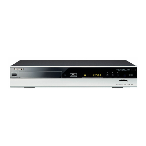
DV-BD606
MODEL
For CMP2P
Black and Silver models
BCMP,SCMP
110-240V AC, 50Hz
SAFETY-RELATED COMPONENT
WARNING!!
COMPONENTS IDENTIFIED BY MARK
SCHEMATIC DIAGRAM AND IN THE PARTS LIST ARE
CRITICAL FOR RISK OF FIRE AND ELECTRIC SHOCK.
REPLACE THESE COMPONENTS WITH ONKYO
PARTS WHOSE PART NUMBERS APPEAR AS SHOWN
IN THIS MANUAL.
MAKE LEAKAGE-CURRENT OR RESISTANCE
MEASUREMENTS TO DETERMINE THAT EXPOSED
PARTS ARE ACCEPTABLY INSULATED FROM THE
SUPPLY CIRCUIT BEFORE RETURNING THE
APPLIANCE TO THE CUSTOMER.
Ref. No. 4115
RC-730DV
ON THE
DV-BD606
102008
Advertisement
Table of Contents

Related Manuals for Onkyo DV-BD606


Summary of Contents for Onkyo DV-BD606
- Page 1 COMPONENTS IDENTIFIED BY MARK ON THE SCHEMATIC DIAGRAM AND IN THE PARTS LIST ARE CRITICAL FOR RISK OF FIRE AND ELECTRIC SHOCK. REPLACE THESE COMPONENTS WITH ONKYO PARTS WHOSE PART NUMBERS APPEAR AS SHOWN IN THIS MANUAL. MAKE LEAKAGE-CURRENT OR RESISTANCE...
-
Page 2: Table Of Contents
TABLE OF CONTENTS Specifications ................1-1-1 Laser Beam Safety Precautions . -
Page 3: Specifications
SPECIFICATIONS 1-1-1 E5J50SP... -
Page 4: Laser Beam Safety Precautions
LASER BEAM SAFETY PRECAUTIONS This BD player uses a pickup that emits a laser beam. Do not look directly at the laser beam coming from the pickup or allow it to strike against your skin. The laser beam is emitted from the location shown in the figure. When checking the laser diode, be sure to keep your eyes at least 30 cm away from the pickup lens when the diode is turned on. -
Page 5: Important Safety Precautions
IMPORTANT SAFETY PRECAUTIONS Product Safety Notice I. Also check areas surrounding repaired locations. J. Use care that foreign objects (screws, solder drop- Some electrical and mechanical parts have special lets, etc.) do not remain inside the set. safety-related characteristics which are often not evi- K. - Page 6 Safety Check after Servicing Chassis or Secondary Conductor Examine the area surrounding the repaired location for damage or deterioration. Observe that screws, parts, and wires have been returned to their original Primary Circuit positions. Afterwards, do the following tests and con- firm the specified values to verify compliance with safety standards.
-
Page 7: Standard Notes For Servicing
STANDARD NOTES FOR SERVICING Circuit Board Indications Pb (Lead) Free Solder 1. The output pin of the 3 pin Regulator ICs is When soldering, be sure to use the Pb free solder. indicated as shown. How to Remove / Install Flat Pack-IC Top View Bottom View 1. - Page 8 3. The flat pack-IC on the CBA is affixed with glue, so With Soldering Iron: be careful not to break or damage the foil of each 1. Using desoldering braid, remove the solder from pin or the solder lands under the IC when all pins of the flat pack-IC.
- Page 9 2. Installation With Iron Wire: 1. Using desoldering braid, remove the solder from 1. Using desoldering braid, remove the solder from all pins of the flat pack-IC. When you use solder the foil of each pin of the flat pack-IC on the CBA flux which is applied to all pins of the flat pack-IC, so you can install a replacement flat pack-IC more you can remove it easily.
- Page 10 Instructions for Handling Semi- conductors Electrostatic breakdown of the semi-conductors may occur due to a potential difference caused by electrostatic charge during unpacking or repair work. 1. Ground for Human Body Be sure to wear a grounding band (1 MΩ) that is properly grounded to remove any static electricity that may be charged on the body.
-
Page 11: Cabinet Disassembly Instructions
CABINET DISASSEMBLY INSTRUCTIONS 1. Disassembly Flowchart Removal Remove/*Unhook/ This flowchart indicates the disassembly steps to gain Loc. Part Fig. Unlock/Release/ Note access to item(s) to be serviced. When reassembling, Unplug/Desolder follow the steps in reverse order. Bend, route, and 2(S-16), (S-17), dress the cables as they were originally. - Page 12 [1] Top Cover (S-1) (S-1) (S-6) (S-5) [6] BE Main CBA Unit CN7401 (S-7) [5] FE Main CN7001 CN6401 CBA& BD Mechanism CN7602 Assembly Locking Card (S-1) Spacers CN2601 Fig. D3 Fig. D1 (S-9) (S-8) (S-8) (S-8) (S-10) [7] Power Supply CBA [4] Power SW CN2001...
- Page 13 CN2004 (S-14) (S-15) (S-14) (S-14) [10] AV CBA (S-19) (S-11) [13] BE PCB (S-13) (S-11) Holder Assembly (S-12) [9] Motor DC Fan (S-11) [8] Rear Panel (S-16) (S-17) (S-18) [12] Front SD Card [11] SD CBA Bracket R Holder Fig. D5 3.
-
Page 14: How To Initialize The Blu-Ray Disc Player
HOW TO INITIALIZE THE BLU-RAY DISC PLAYER To put the program back at the factory-default, initialize the BD player as the following procedure. 1. Turn the power on. 2. Remove the disc on the tray and close the tray. 3. Press [1], [2], [3], [4], and [DISPLAY] buttons on the remote control unit in that order. -
Page 15: Firmware Renewal Mode
FIRMWARE RENEWAL MODE 1. Turn the power on and remove the disc on the tray. The appearance shown in (*1) of Fig. c is described as follows: 2. To put the BD player into version up mode, press [9], [8], [7], [6], and [POP UP MENU/MENU] Appearance State buttons on the remote control unit in that order. - Page 16 How to Verify the Firmware Version 9. Press [STOP] button on the remote control unit. Fig. h appears on the screen and Fig. i appears on 1. Turn the power on. the VFD. 2. Remove the disc on the tray and close the tray. "...
-
Page 17: Block Diagrams
BLOCK DIAGRAMS System Control Block Diagram 1-8-1 E5J50BLS... - Page 18 Digital Signal Process 1 Block Diagram 1-8-2 E5J50BLD1...
- Page 19 Digital Signal Process 2 Block Diagram 1-8-3 E5J50BLD2...
- Page 20 Video Block Diagram TMDS SERIALIZER TMDS ENCODER HDCP CIPHER/ ENCRYPTOR CONTROLLER AUDIO 1-8-4 E5J50BLV...
- Page 21 Audio Block Diagram 1-8-5 E5J50BLA...
- Page 22 Power Supply Block Diagram 1-8-6 E5J50BLP...
-
Page 23: Schematic Diagrams / Cba And Test Points
SCHEMATIC DIAGRAMS / CBA AND TEST POINTS Standard Notes WARNING Many electrical and mechanical parts in this chassis have special characteristics. These characteristics often pass unnoticed and the protection afforded by them cannot necessarily be obtained by using replacement components rated for higher voltage, wattage, etc. - Page 24 LIST OF CAUTION, NOTES, AND SYMBOLS USED IN THE SCHEMATIC DIAGRAMS ON THE FOLLOWING PAGES: 1. CAUTION: FOR CONTINUED PROTECTION AGAINST FIRE HAZARD, REPLACE ONLY WITH THE SAME TYPE FUSE. 2. CAUTION: Fixed Voltage (or Auto voltage selectable) power supply circuit is used in this unit. If Main Fuse (F1001) is blown, first check to see that all components in the power supply circuit are not defective before you connect the AC plug to the AC power supply.
- Page 25 AV 1/3 Schematic Diagram * NOTE These components (IC2001, C2013) can be used in any models. However, you cannot mix components under Group A with the ones under Group B. You can choose either Group. The difference between Group A and Group B is shown below. Group A Group B IC2001...
- Page 26 AV 2/3 Schematic Diagram 1-9-4 E5J50SCAV2...
- Page 27 AV 3/3 Schematic Diagram 1-9-5 E5J50SCAV3...
- Page 28 Power Supply Schematic Diagram CAUTION ! NOTE: CAUTION ! Fixed voltage (or Auto voltage selectable) power supply circuit is used in this unit. For continued protection against fire hazard, The voltage for parts in hot circuit is measured using If Main Fuse (F1001) is blown , check to see that all components in the power supply replace only with the same type fuse.
- Page 29 Front & Power SW Schematic Diagram 1-9-7 E5J50SCF...
- Page 30 SD Schematic Diagram 1-9-8 E5J50SCSD...
- Page 31 FE Main 1/5 Schematic Diagram 1 NOTE: The order of pins shown in this diagram is different from that of actual IC001. IC001 is divided into four and shown as IC001 (1/4) ~ IC001 (4/4) in this FE Main Schematic Diagram Section. 1-9-9 E5J50SCFM1...
- Page 32 FE Main 2/5 Schematic Diagram 1 NOTE: The order of pins shown in this diagram is different from that of actual IC001. IC001 is divided into four and shown as IC001 (1/4) ~ IC001 (4/4) in this FE Main Schematic Diagram Section. 1-9-10 E5J50SCFM2...
- Page 33 FE Main 3/5 Schematic Diagram 1-9-11 E5J50SCFM3...
- Page 34 FE Main 4/5 Schematic Diagram 1 NOTE: The order of pins shown in this diagram is different from that of actual IC001. IC001 is divided into four and shown as IC001 (1/4) ~ IC001 (4/4) in this FE Main Schematic Diagram Section. 1-9-12 E5J50SCFM4...
- Page 35 FE Main 5/5 Schematic Diagram 1 NOTE: The order of pins shown in this diagram is different from that of actual IC001. IC001 is divided into four and shown as IC001 (1/4) ~ IC001 (4/4) in this FE Main Schematic Diagram Section. 1-9-13 E5J50SCFM5...
- Page 36 BE Main 1/10 Schematic Diagram 2 NOTE: The order of pins shown in this diagram is different from that of actual IC6001. IC6001 is divided into eight and shown as IC6001 (1/8) ~ IC6001 (8/8) in this BE Main Schematic Diagram Section. 1-9-14 E5J50SCBM1...
- Page 37 BE Main 2/10 Schematic Diagram 2 NOTE: The order of pins shown in this diagram is different from that of actual IC6001. IC6001 is divided into eight and shown as IC6001 (1/8) ~ IC6001 (8/8) in this BE Main Schematic Diagram Section. 1-9-15 E5J50SCBM2...
- Page 38 BE Main 3/10 Schematic Diagram 2 NOTE: The order of pins shown in this diagram is different from that of actual IC6001. IC6001 is divided into eight and shown as IC6001 (1/8) ~ IC6001 (8/8) in this BE Main Schematic Diagram Section. 1-9-16 E5J50SCBM3...
- Page 39 BE Main 4/10 Schematic Diagram 2 NOTE: The order of pins shown in this diagram is different from that of actual IC6001. IC6001 is divided into eight and shown as IC6001 (1/8) ~ IC6001 (8/8) in this BE Main Schematic Diagram Section. 1-9-17 E5J50SCBM4...
- Page 40 BE Main 5/10 Schematic Diagram 2 NOTE: The order of pins shown in this diagram is different from that of actual IC6001. IC6001 is divided into eight and shown as IC6001 (1/8) ~ IC6001 (8/8) in this BE Main Schematic Diagram Section. 1-9-18 E5J50SCBM5...
- Page 41 BE Main 6/10 Schematic Diagram 2 NOTE: The order of pins shown in this diagram is different from that of actual IC6001. IC6001 is divided into eight and shown as IC6001 (1/8) ~ IC6001 (8/8) in this BE Main Schematic Diagram Section. 1-9-19 E5J50SCBM6...
- Page 42 BE Main 7/10 Schematic Diagram 2 NOTE: The order of pins shown in this diagram is different from that of actual IC6001. IC6001 is divided into eight and shown as IC6001 (1/8) ~ IC6001 (8/8) in this BE Main Schematic Diagram Section. 1-9-20 E5J50SCBM7...
- Page 43 BE Main 8/10 Schematic Diagram 2 NOTE: The order of pins shown in this diagram is different from that of actual IC6001. IC6001 is divided into eight and shown as IC6001 (1/8) ~ IC6001 (8/8) in this BE Main Schematic Diagram Section. 1-9-21 E5J50SCBM8...
- Page 44 BE Main 9/10 Schematic Diagram E5J50SCBM9 1-9-22...
- Page 45 BE Main 10/10 Schematic Diagram 1-9-23 E5J50SCBM10...
- Page 46 AV CBA Top View BE5J10F01072A 1-9-24...
- Page 47 AV CBA Bottom View BE5J10F01072A 1-9-25...
- Page 48 Power Supply CBA Top View CAUTION ! NOTE: CAUTION ! For continued protection against fire hazard, The voltage for parts in hot circuit is measured using Fixed voltage (or Auto voltage selectable) power supply circuit is used in this unit. replace only with the same type fuse.
- Page 49 Power Supply CBA Bottom View CAUTION ! NOTE: CAUTION ! For continued protection against fire hazard, The voltage for parts in hot circuit is measured using Fixed voltage (or Auto voltage selectable) power supply circuit is used in this unit. replace only with the same type fuse.
- Page 50 Front CBA Top View SD CBA Bottom View BE5E20F01042 Power SW CBA Power SW CBA Front CBA Bottom View Top View Bottom View BE5J10F01072B BE5J10F01072C 1-9-28...
-
Page 51: Exploded Views
EXPLODED VIEWS Cabinet 2L082 2L082 See Electrical Parts List for parts with this mark. 2L082 Some Ref. Numbers are 2L082 not in sequence. Power Supply CBA 2L047 2L015 2L027 F1001 2L082 2L027 BE Main CBA Unit 2L082 FE Main CBA & BD Mechanism 2L034 Assembly... - Page 52 Packing Upper Side Lower Side X2-A X2-B X2-C X2-D X1-A X1-B X1-C Some Ref. Numbers are not in sequence. 1-10-2 E5J50PEX...
-
Page 53: Mechanical Parts List
UNIT BAG E5500UD 0VM411683 Comparison Chart of Models and Marks ACCESSORIES X1-A! OWNERS MANUAL(EN) E5J50ED 1VMN26504 Model Mark X1-B! OWNERS MANUAL(ES) E5J50ED 1VMN26505 DV-BD606(B)CMP X1-C! OWNERS MANUAL(FR) E5J50ED 1VMN26506 DV-BD606(S)CMP X2-A QUICK GUIDE(EN) E5J50ED 1VMN26507 X2-B QUICK GUIDE(ES/FR) E5J50ED 1VMN26508 X2-C... -
Page 54: Electrical Parts List
ELECTRICAL PARTS LIST PRODUCT SAFETY NOTE: Products marked with a Ref. No. Description Part No. ! have special characteristics important to safety. C2107 ELECTROLYTIC CAP . 220µF/6.3V M CE0KMASDL221 Before replacing any of these components, read C2108 CHIP CERAMIC CAP .(1608) F Z 0.1µF/50V CHD1JZ30F104 carefully the product safety notice in this service C2180... - Page 55 Ref. No. Description Part No. Ref. No. Description Part No. D2003 DIODE ZENER 36BSA-T26 NDTA036BST26 Q2605 TRANSISTOR KTC3203-Y-AT/P NQSYKTC3203P D2004 DIODE SWITCHING 1N4148-F0021 NDTZ01N4148F Q2606 TRANSISTOR KTA1273-Y -AT/P NQSYKTA1273P D2005 DIODE ZENER 12BSB-T26 NDTB012BST26 Q2607 TRANSISTOR(PB FREE) KTC2026-Y/P NQEYKTC2026P D2006 DIODE SWITCHING 1N4148-F0021 NDTZ01N4148F RESISTORS...
- Page 56 Ref. No. Description Part No. Ref. No. Description Part No. CHIP RES. 1/10W J 270 Ω R2124 RRXAJR5Z0271 MISCELLANEOUS CHIP RES. 1/10W J 270 Ω R2125 RRXAJR5Z0271 2L055 SCREW S-TIGHT M3X8 BIND HEAD+ GBJS3080 CHIP RES.(1608) 1/10W 0 Ω R2126 RRXAZR5Z0000 POWER HEATSINK E4340UD 1VM422057E...
- Page 57 Ref. No. Description Part No. Ref. No. Description Part No. RS3000 SENSOR REMOTE RECEIVER KSM-713TH2E USESJRSKK046 D1022 SCHOTTKY BARRIER DIODE SB140 NDQZ000SB140 D1023 SCHOTTKY BARRIER DIODE SB3B0 NDQZ000SB3B0 POWER SUPPLY CBA D1025 DIODE SWITCHING 1N4148-F0021 NDTZ01N4148F D1026 DIODE SWITCHING 1N4148-F0021 NDTZ01N4148F Ref.
- Page 58 Ref. No. Description Part No. CHIP RES. 1/10W F 82.0 k Ω R1047 RRXAFR5H8202 CHIP RES. 1/10W F 100k Ω R1048 RRXAFR5H1003 METAL RESISTER. 2W J 2.7 Ω R1050 RN022R7ZU001 CARBON RES. 1/4W J 470k Ω R1051 RCX4JATZ0474 CARBON RES. 1/4W J 470k Ω R1052 RCX4JATZ0474 CHIP RES.(1608) 1/10W 0 Ω...
- Page 59 Sales & Product Planning Div. : 2-1, Nisshin-cho, Neyagawa-shi, OSAKA 572-8540, JAPAN Tel: 072-831-8023 Fax: 072-831-8163 ONKYO U.S.A. CORPORATION 18 Park Way, Upper Saddle River, N.J. 07458, U.S.A. Tel: 201-785-2600 Fax: 201-785-2650 http://www.us.onkyo.com/ ONKYO EUROPE ELECTRONICS GmbH Liegnitzerstrasse 6, 82194 Groebenzell, GERMANY Tel: +49-8142-4401-0 Fax: +49-8142-4401-555 http://www.eu.onkyo.com/...
Need help?
Do you have a question about the DV-BD606 and is the answer not in the manual?
Questions and answers