Table of Contents
Advertisement
QQ
3 7 63 1515 0
SERVICE MANUAL
Ver. 1.0 2005.06
• HCD-AZ2D is the amplifier, disc player, tape
deck and tuner section in DHC-AZ2D.
• HCD-AZ5D is the amplifier, disc player tape
deck and tuner section in DHC-AZ5D.
This system incorporates Dolby
Logic (II) adaptive matrix surround decoder, and
2)
DTS
Digital Surround System.
1)
Manufactured under license from Dolby
Laboratories.
"Dolby", "Pro Logic", and the double-D symbol are
trademarks of Dolby Laboratories.
2)
Manufactured under license from Digital Theater
TE
L 13942296513
Systems, Inc. "DTS" and "DTS Digital Surround"
are registered trademarks of Digital Theater
Systems, Inc.
Amplifier section
HCD-AZ5D
The following measured at AC 120, 127, 220, 240 V,
50/60 Hz
DIN power output (rated): 75 + 75 watts
Continuous RMS power output (reference)
Front speaker:
Center speaker:
Surround speaker:
Subwoofer:
HCD-AZ2D
The following measured at AC 120, 127, 220, 240 V,
50/60 Hz
DIN power output (rated): 75 + 75 watts
Continuous RMS power output (reference)
Inputs
www
VIDEO/SAT IN (audio) (phono jacks):
.
Sony Corporation
9-879-718-01
Audio Group
2005F0579-1
Published by Sony Engineering Corporation
© 2005.06
http://www.xiaoyu163.com
HCD-AZ2D/AZ5D
1)
Digital, Dolby Pro
MIC 1/MIC 2 (phone jacks):
Outputs
VIDEO/SAT OUT (audio) (phono jacks):
(4 ohms at 1 kHz, DIN)
VIDEO OUT (phono jack):
100 + 100 watts
(4 ohms at 1 kHz, 10%
THD)
50 watts (8 ohms at 1 kHz,
10% THD)
S VIDEO OUT (4-pin/mini-DIN jack):
50 + 50 watts
(8 ohms at 1 kHz, 10%
THD)
180 watts (2 ohms at
100 Hz, 10% THD)
COMPONENT VIDEO OUT:
DVD DIGITAL OUT (DHC-AZ2D only)
(Square optical connector jack, rear panel)
Wavelength
(4 ohms at 1 kHz, DIN)
PHONES (stereo mini jack):
100 + 100 watts
(4 ohms at 1 kHz, 10%
FRONT SPEAKER:
THD)
SURROUND SPEAKER (HCD-AZ5D only):
voltage 250/450 mV,
x
ao
y
impedance 47 kilohms
i
http://www.xiaoyu163.com
8
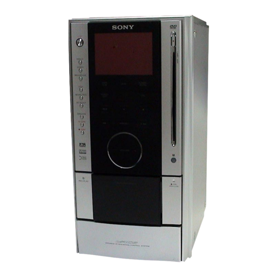
Photo: HCD-AZ5D
Model Name Using Similar Mechanism
DVD
DVD Mechanism Type
Section
Optical Pick-up Block Name
Tape deck-A
Model Name Using Similar Mechanism
Section
Tape Transport Mechanism Type
Q Q
Tape deck-B
Model Name Using Similar Mechanism
3
6 7
1 3
Section
Tape Transport Mechanism Type
SPECIFICATIONS
sensitivity 1 mV,
impedance 10 kilohms
voltage 250 mV,
impedance 1 kilohm
max. output level
1 Vp-p, unbalanced, Sync
negative, load impedance
75 ohms
Y: 1 Vp-p, unbalanced,
Sync negative,
C: 0.286 Vp-p, load
impedance 75 ohms
Y: 1 Vp-p, 75 ohms
P
, P
: 0.7 Vp-p, 75 ohms
B
R
660 nm
accepts headphones of
8 ohms or more
Use only the supplied
speaker SS-AZ7D.
Use only the supplied
u163
speaker SS-RS7D.
.
2 9
9 4
2 8
Australian Model
1 5
0 5
8
2 9
9 4
CENTER SPEAKER (HCD-AZ5D only):
SUBWOOFER (HCD-AZ5D only):
Disc player section
System
Laser
Frequency response
Video color system format
– Continued on next page –
m
DVD DECK RECEIVER
co
9 9
E Model
NEW
CDM86-DVBU101
KHM-310CAB
NEW
CMAL5Z230
NEW
2 8
9 9
CMAL1Z254A
Use only the supplied
speaker SS-CT7D.
Use only the supplied
speaker SS-WG7D.
Compact disc and digital
audio and video system
Semiconductor laser
(DVD: λ =650 nm,
CD: λ =790 nm)
Emission duration:
continuous
DVD (PCM 48 kHz):
2 Hz − 22 kHz (±1 dB)
CD: 2 Hz − 20 kHz (±1 dB)
Latin American model:
NTSC
Other models: NTSC, PAL
Advertisement
Table of Contents

Related Manuals for Sony HCD-AZ2D


Summary of Contents for Sony HCD-AZ2D
-
Page 1: Service Manual
3 7 63 1515 0 SERVICE MANUAL E Model Australian Model Ver. 1.0 2005.06 • HCD-AZ2D is the amplifier, disc player, tape deck and tuner section in DHC-AZ2D. • HCD-AZ5D is the amplifier, disc player tape deck and tuner section in DHC-AZ5D. Photo: HCD-AZ5D... -
Page 2: Self Diagnosis Function
COMPONENTS IDENTIFIED BY MARK 0 OR DOTTED LINE WITH MARK 0 ON THE SCHEMATIC DIAGRAMS AND IN THE PARTS LIST ARE CRITICAL TO SAFE OPERATION. REPLACE THESE COMPONENTS WITH SONY PARTS WHOSE PART NUMBERS APPEAR AS SHOWN IN THIS MANUAL OR IN SUPPLEMENTS PUBLISHED BY SONY. -
Page 3: Playable Discs
HCD-AZ2D/AZ5D 3 7 63 1515 0 • DVD-ROMs/DVD-Rs/DVD-RWs/DVD+Rs/ Playable discs Cautions when playing a disc DVD+RWs recorded in Multi Session that is recorded in Multi • DVD-RAMs You can play back the following discs on this • DVD Audio discs Session system. -
Page 4: Table Of Contents
HCD-AZ2D/AZ5D 3 7 63 1515 0 TABLE OF CONTENTS SERVICING NOTES 7-12. Printed Wiring Board – MS-214 Board – ...... 39 ..........5 7-13. Schematic Diagram – MS-214 Board – ......39 7-14. Printed Wiring Board – MAIN Board – ......40 GENERAL .............. -
Page 5: Servicing Notes
(LF) indicating the solder contains no lead. (Caution: Some printed circuit boards may not come printed with the lead free mark due to their particular size) Model PART No. HCD-AZ2D: SP, MY 2-349-677-0[] : LEAD FREE MARK HCD-AZ2D: E2 2-349-677-1[] Unleaded solder has the following characteristics. - Page 6 HCD-AZ2D/AZ5D 3 7 63 1515 0 TAPE MECH DECK (CMAL5Z230) (DECK-A) SERVICE POSITION tape mech deck (CMAL5Z230) (deck-A) top panel (TC) section L 13942296513 TAPE MECH DECK (CMAL1Z254A) (DECK-B) SERVICE POSITION u163 tape mech deck (CMAL1Z254A) (deck-B) http://www.xiaoyu163.com...
- Page 7 HCD-AZ2D/AZ5D 3 7 63 1515 0 DVD MECHANISM DECK (CDM86-DVBU101) SERVICE POSITION • In checking the DVD mechanism deck (CDM86-DVBU101), prepare extension jig (Part No. J-2501-241-A: 1.00mm pitch, 7 cores, length 300mm). Connect extension jig (J-2501-241-A) to the MS-214 board (CN001) and DVB10 board (CN202).
- Page 8 HCD-AZ2D/AZ5D 3 7 63 1515 0 S-MASTER BOARD SERVICE POSITION • In checking the S-MASTER board, prepare extension jig (Part No. J-2501-082-A: 1.25mm pitch, 9 cores, length 300mm). Connect extension jig (J-2501-082-A) to the S-MASTER board (CN502) and MAIN board (CN102).
-
Page 9: General
HCD-AZ2D/AZ5D SECTION 2 This section is extracted from instruction manual. GENERAL 3 7 63 1515 0 LOCATION OF CONTROLS Main unit BUTTON DESCRIPTIONS ALPHABETICAL ORDER ?/1 (power) 1 M – Z A – N Z PUSH OPEN/CLOSE (deck A) -
Page 10: Setting The Clock
HCD-AZ2D/AZ5D 3 7 63 1515 0 Remote control ALPHABETICAL ORDER BUTTON DESCRIPTIONS ?/1 (power) 1 A – Q R – Z TV ?/1 1 ALBUM +/− wf REPEAT ws REPLAY/ADVANCE ANGLE 5 SLEEP qk AUDIO 4 SOUND FIELD wa... -
Page 11: Disassembly
HCD-AZ2D/AZ5D SECTION 3 DISASSEMBLY 3 7 63 1515 0 • This set can be disassembled in the order shown below. 3-1. DISASSEMBLY FLOW 3-2. SIDE PANEL (A)/(B) (Page 12) 3-3. FRONT PANEL SECTION 3-8. DVD MECHANISM DECK (Page 12) -
Page 12: Side Panel (A)/(B)
HCD-AZ2D/AZ5D 3 7 63 1515 0 Note: Follow the disassembly procedure in the numerical order given. 3-2. SIDE PANEL (A)/(B) 2 three screws 5 side panel (A) (BVTP 3 × 8) 9 side panel (B) 7 three screws (BVTP 3 × 8) -
Page 13: Tape Mech Deck (Cmal1Z254A) (Deck-B)
HCD-AZ2D/AZ5D 3 7 63 1515 0 3-4. TAPE MECH DECK (CMAL1Z254A) (DECK-B) 6 wire (flat type) (8 core) 3 two screws (BVTP 2.6) 2 cover (TCM B) 1 two screws (BVTP 2.6) 3 two screws (BVTP 2.6) 4 ground wire 7 tape mech deck (CMAL1Z254A) (deck-B) 3-5. -
Page 14: Tape Mech Deck (Cmal5Z230) (Deck-A)
HCD-AZ2D/AZ5D 3 7 63 1515 0 3-6. TAPE MECH DECK (CMAL5Z230) (DECK-A) 6 tape mech deck (CMAL5Z230) (deck-A) 4 two screws (BVTP 2.6) 5 ground wire 3 wire (flat type) (7 core) 4 two screws (BVTP 2.6) 2 cover (TCM A) 1 three screws (BVTP 2.6) -
Page 15: Dvd Mechanism Deck (Cdm86-Dvbu101)
HCD-AZ2D/AZ5D 3 7 63 1515 0 3-8. DVD MECHANISM DECK (CDM86-DVBU101) CAUTION 9 Be sure to execute a solder bridge as a measure against static electricity when removing the OP block (DVBU101). (Otherwise, the OP block will be destroyed.) 8 Lift up the FFC holder. -
Page 16: Optical Pick-Up Block (Khm-310Cab)
HCD-AZ2D/AZ5D 3 7 63 1515 0 3-9. OPTICAL PICK-UP BLOCK (KHM-310CAB) 3 optical pick-up block (KHM-310CAB) 2 two insulators 2 two insulators 1 two insulator screws 1 two insulator screws 3-10. MOTOR (PULLEY) ASSY (LOADING) (M001) L 13942296513 2 two screws (B 2.6 ×... -
Page 17: Holder (Bu) Assy
HCD-AZ2D/AZ5D 3 7 63 1515 0 3-11. HOLDER (BU) ASSY 1 screw (B 2.6 × 8) 2 lever (CL UP2) 6 holder (BU) assy 4 LHL support 5 floating screw (PTPWH M2.6) 3 two screws (B 2 × 6) 5 floating screw (PTPWH M2.6) -
Page 18: Close Lever
HCD-AZ2D/AZ5D 3 7 63 1515 0 3-13. CLOSE LEVER 1 washer (3-1-0.4) 5 close lever 3 claw 2 SPR-E lever close 4 shaft disc stop L 13942296513 3-14. LEVER (DIR), GEAR (IDL-B) 3 nylon washer 1.7 2 claw 4 pulley (gear) -
Page 19: Chassis (Top)
HCD-AZ2D/AZ5D 3 7 63 1515 0 3-15. CHASSIS (TOP) 4 three screws 1 screw (B 2.6 × 8) (B 2.6 × 8) 3 two screws (B 2 × 10) 2 lever (CL UP2) 5 chassis (top) L 13942296513 u163... -
Page 20: Lever (Loading-L/R)
HCD-AZ2D/AZ5D 3 7 63 1515 0 3-16. LEVER (LOADING-L/R) SPT-T (loading-R) SPR-T (loading-L) 5 lever (loading-R) L 13942296513 2 two hooks 4 two hooks 3 lever (loading-L) PRECAUTION DURING LEVER (LOADING R / L) INSTALLATION BOTTOM VIEW Align the horizontal position. -
Page 21: Lever (Disc Sensor)/(Disc Stop)
HCD-AZ2D/AZ5D 3 7 63 1515 0 3-17. LEVER (DISC SENSOR)/(DISC STOP) 1 gear (cap) 2 gear (IDL L) PRECAUTION DURING DISC STOP LEVER INSTALLATION chassis (top) hole 5 two hooks 3 two claws lever (disc stop) 6 lever (disc stop) -
Page 22: Test Mode
HCD-AZ2D/AZ5D SECTION 4 TEST MODE 3 7 63 1515 0 COLD RESET DISC SLOT LOCK The cold reset clears data except DVD data stored in the RAM to This mode let you lock the disc slot. When this mode is activated, initial conditions. - Page 23 HCD-AZ2D/AZ5D 3 7 63 1515 0 4. MIRROR TIME ADJUSTMENT DVD SECTION On the Drive Manual Operation menu screen, press [5] button on the remote commander, and the following MIRR time Adjust Menu 1. DVD SERVICE MODE GENERAL DESCRIPTION will be displayed.
- Page 24 HCD-AZ2D/AZ5D 3 7 63 1515 0 17. Take out the CD test disc (YEDS-18) 18. Release the MIRR time Adjust Menu mode. MIRR time Adjust Menu 5. EXECUTING IOP MEASUREMENT 1. CD MIRR time Check: In order to execute IOP measurement, the following standard 2.
-
Page 25: Mechanical Adjustments
HCD-AZ2D/AZ5D SECTION 5 SECTION 6 MECHANICAL ADJUSTMENTS ELECTRICAL ADJUSTMENTS 3 7 63 1515 0 PRECAUTION DECK SECTION 0 dB=0.775 V 1. Clean the following parts with a denatured-alcohol-moistened swab : 1. Demagnetize the record/playback head with a head record/playback head pinch roller demagnetizer. - Page 26 HCD-AZ2D/AZ5D 3 7 63 1515 0 3. Mode: Playback DVD SECTION test tape MAIN board RFMON LEVEL CHECK P-4-A063 oscilloscope VIDEO/SAT OUT (6.3 kHz, –10 dB) jack (J101) oscilloscope (DC range) DMB10 board CN105 pin 6 (RFMON) CN105 pin 3 (GND) –...
-
Page 27: Diagrams
HCD-AZ2D/AZ5D SECTION 7 3 7 6 3 1 5 1 5 0 DIAGRAMS 7-1. BLOCK DIAGRAM – RF SERVO/VIDEO SECTION – ASDATA0 217 SDTI1 LOUT1+ 2 FL, FR, SL, SR, FC, SW, LT, RT LOUT1– 1 MIX AMP DVDRF IP... -
Page 28: Block Diagram - Tuner/Tape Section
HCD-AZ2D/AZ5D 3 7 6 3 1 5 1 5 0 7-2. BLOCK DIAGRAM – TUNER/TAPE SECTION – ANTENNA TUNER UNIT ST-L FM 75Ω FM ANT ST-L COAXIAL ST-R R-CH (Page 29) AM ANT STDOUT 40 ST-DIN STDIN 38 ST-DOUT... -
Page 29: Block Diagram - Audio Section
HCD-AZ2D/AZ5D 3 7 6 3 1 5 1 5 0 7-3. BLOCK DIAGRAM – AUDIO SECTION – J101 (2/2) VIDEO/SAT USB D/A R-CH CONVERTER (Page 28) REC-L 9 D+ VOUTL SPDATA, ACLK, D– 8 D– VOUTR R-CH ABCK, ALRCK... -
Page 30: Block Diagram - Amp Section
HCD-AZ2D/AZ5D 3 7 6 3 1 5 1 5 0 7-4. BLOCK DIAGRAM – AMP SECTION – A/D CONVERTER D771 IC503 STREAM PROCESSOR DIGITAL POWER AMP FEED BACK IC506 IC512 FL, FR, SL, SR, C, SW (Page 29) DOUT... -
Page 31: Block Diagram - Panel/Power Supply Section
HCD-AZ2D/AZ5D 3 7 6 3 1 5 1 5 0 7-5. BLOCK DIAGRAM – PANEL/POWER SUPPLY SECTION – +1.8V +1.8V REGULATOR IC518 +3.3V D+3.3V REGULATOR (FOR AMP SECTION) IC517 D953 A+5V REGULATOR IC516 T101 DC/DC A+9V REGULATOR CONVERTER IC951... - Page 32 HCD-AZ2D/AZ5D 3 7 6 3 1 5 1 5 0 • Note for Printed Wiring Boards and Schematic Diagrams • Circuit Boards Location Note on Printed Wiring Board: Note on Schematic Diagram: • X : parts extracted from the component side.
-
Page 33: Printed Wiring Board - Dmb10 Board (Side A)
HCD-AZ2D/AZ5D • See page 32 for Circuit Boards Location. 3 7 6 3 1 5 1 5 0 7-6. PRINTED WIRING BOARD – DMB10 BOARD (SIDE A) – : Uses unleaded solder. MAIN BOARD NO953 DMB10 BOARD (SIDE A) (Page 40) •... -
Page 34: Printed Wiring Board - Dmb10 Board (Side B)
HCD-AZ2D/AZ5D 3 7 6 3 1 5 1 5 0 • See page 32 for Circuit Boards Location. 7-7. PRINTED WIRING BOARD – DMB10 BOARD (SIDE B) – : Uses unleaded solder. DMB10 BOARD (SIDE B) • Semiconductor Location (AZ5D) Ref. -
Page 35: Schematic Diagram - Dmb10 Board (1/4)
HCD-AZ2D/AZ5D 3 7 6 3 1 5 1 5 0 • See page 60 for IC Block Diagrams. 7-8. SCHEMATIC DIAGRAM – DMB10 BOARD (1/4) – (Page 37) (1/4) EEPROM IC103 BR24L64F-WE2 C167 CN106 0.01 R193 OCSW1 (Page 37) R1546 3.3k... -
Page 36: Schematic Diagram - Dmb10 Board (2/4)
HCD-AZ2D/AZ5D 3 7 6 3 1 5 1 5 0 7-9. SCHEMATIC DIAGRAM – DMB10 BOARD (2/4) – R223 100k (2/4) R225 100k (Page 44) CN401 IOPMON FB402 FL401 FB404 VREFO SW+5V SW+5V C233 0.0047 R220 SPFG D-GND FB403... -
Page 37: Schematic Diagram - Dmb10 Board (3/4)
HCD-AZ2D/AZ5D 3 7 6 3 1 5 1 5 0 • See page 59 for Waveforms. • See page 67 for IC Pin Function Description. 7-10. SCHEMATIC DIAGRAM – DMB10 BOARD (3/4) – (Page 38) (Page 35) R1120 (3/4) -
Page 38: Schematic Diagram - Dmb10 Board (4/4)
HCD-AZ2D/AZ5D 3 7 6 3 1 5 1 5 0 • See page 60 for IC Block Diagrams. 7-11. SCHEMATIC DIAGRAM – DMB10 BOARD (4/4) – R3781 R3783 R3788 (4/4) 1.5k 3.9k 4.7k ART- C3781 C3782 R3786 R3787 0.0018 0.0022... -
Page 39: Printed Wiring Board - Ms-214 Board
HCD-AZ2D/AZ5D 3 7 6 3 1 5 1 5 0 7-13. SCHEMATIC DIAGRAM – MS-214 BOARD – 7-12. PRINTED WIRING BOARD – MS-214 BOARD – • See page 32 for Circuit Boards Location. : Uses unleaded solder. MS-214 BOARD... -
Page 40: Printed Wiring Board - Main Board
HCD-AZ2D/AZ5D 3 7 6 3 1 5 1 5 0 • See page 32 for Circuit Boards Location. 7-14. PRINTED WIRING BOARD – MAIN BOARD – : Uses unleaded solder. • Semiconductor Location Ref. No. Location Ref. No. Location... -
Page 41: Schematic Diagram - Main Board (1/4)
HCD-AZ2D/AZ5D 3 7 6 3 1 5 1 5 0 • See page 60 for IC Block Diagrams. 7-15. SCHEMATIC DIAGRAM – MAIN BOARD (1/4) – ANTENNA FM 75Ω COAXIAL TUNER UNIT SUPPLIED WITH THE ASSEMBLED BLOCK (Page 38) -
Page 42: Schematic Diagram - Main Board (2/4)
HCD-AZ2D/AZ5D 3 7 6 3 1 5 1 5 0 • See page 59 for Waveforms. 7-16. SCHEMATIC DIAGRAM – MAIN BOARD (2/4) – (Page 41) (Page 41) (2/4) C106 10 50V C109 R104 2.2k (Page 44) R103 2.2k... -
Page 43: Schematic Diagram - Main Board (3/4)
HCD-AZ2D/AZ5D 3 7 6 3 1 5 1 5 0 • See page 59 for Waveforms. • See page 72 for IC Pin Function Description. 7-17. SCHEMATIC DIAGRAM – MAIN BOARD (3/4) – C464 C462 (3/4) 100 10V Q465... -
Page 44: Schematic Diagram - Main Board (4/4)
HCD-AZ2D/AZ5D 3 7 6 3 1 5 1 5 0 7-18. SCHEMATIC DIAGRAM – MAIN BOARD (4/4) – (Page 43) (Page 42) (4/4) CN203 OCSW1 SYSRST 3.3V_MNT C260 2200p (AZ5D:EA,AUS) XIFCS IFBSY MREQ (Page 35) D-GND +9V REGULATOR +9V REGULATOR... -
Page 45: Printed Wiring Board - S-Master Board (Component Side)
HCD-AZ2D/AZ5D 3 7 6 3 1 5 1 5 0 • See page 32 for Circuit Boards Location. 7-19. PRINTED WIRING BOARD – S-MASTER BOARD (COMPONENT SIDE) – : Uses unleaded solder. • Semiconductor Location Ref. No. Location D501... -
Page 46: Printed Wiring Board - S-Master Board (Conductor Side)
HCD-AZ2D/AZ5D 3 7 6 3 1 5 1 5 0 • See page 32 for Circuit Boards Location. 7-20. PRINTED WIRING BOARD – S-MASTER BOARD (CONDUCTOR SIDE) – : Uses unleaded solder. SP OUT BOARD SP OUT BOARD SP OUT BOARD... -
Page 47: Schematic Diagram - S-Master Board (1/4)
HCD-AZ2D/AZ5D 3 7 6 3 1 5 1 5 0 • See page 59 for Waveforms. • See page 64 for IC Block Diagrams. 7-21. SCHEMATIC DIAGRAM – S-MASTER BOARD (1/4) – (Page 48) (1/4) D507 D508 C656 1SS355TE-17... -
Page 48: Schematic Diagram - S-Master Board (2/4)
HCD-AZ2D/AZ5D 3 7 6 3 1 5 1 5 0 • See page 59 for Waveforms. • See page 62 for IC Block Diagrams. 7-22. SCHEMATIC DIAGRAM – S-MASTER BOARD (2/4) – (Page 50) (2/4) C628 NSP MUTE NSP MUTE... -
Page 49: Schematic Diagram - S-Master Board (3/4)
HCD-AZ2D/AZ5D 3 7 6 3 1 5 1 5 0 • See page 61, 63 for IC Block Diagrams. 7-23. SCHEMATIC DIAGRAM – S-MASTER BOARD (3/4) – (Page 50) R748 R747 Q692 L663 R678 2SA1602 4.7k 10µH C661 C662... -
Page 50: Schematic Diagram - S-Master Board (4/4)
HCD-AZ2D/AZ5D 3 7 6 3 1 5 1 5 0 • See page 61 for IC Block Diagrams. 7-24. SCHEMATIC DIAGRAM – S-MASTER BOARD (4/4) – (4/4) DIGITAL POWER AMP C583 IC507 CXD9775M (CHASSIS) EP503 R572 R585 R573 C582 C585 0.033... -
Page 51: Printed Wiring Board - Mic Board
HCD-AZ2D/AZ5D 3 7 6 3 1 5 1 5 0 • See page 32 for Circuit Boards Location. 7-25. PRINTED WIRING BOARD – MIC BOARD – : Uses unleaded solder. MIC BOARD EP1050 (CHASSIS) (CHASSIS) EP1060 JW1067 C1074 JW1114... -
Page 52: Schematic Diagram - Mic Board
HCD-AZ2D/AZ5D 3 7 6 3 1 5 1 5 0 • See page 64 for IC Block Diagrams. 7-26. SCHEMATIC DIAGRAM – MIC BOARD – C1060 0.22 R1060 J1060 MIC 1 R1061 C1061 0.01 C1070 100p R1075 R1069 150k... -
Page 53: Printed Wiring Boards - Output Section
HCD-AZ2D/AZ5D 3 7 6 3 1 5 1 5 0 • See page 32 for Circuit Boards Location. 7-27. PRINTED WIRING BOARDS – OUTPUT SECTION – : Uses unleaded solder. VIDEO BOARD SP OUT BOARD (AZ5D) JW1105 C1141 (CHASSIS) -
Page 54: Schematic Diagram - Output Section
HCD-AZ2D/AZ5D 3 7 6 3 1 5 1 5 0 • See page 59 for Waveforms. • See page 66 for IC Block Diagrams. 7-28. SCHEMATIC DIAGRAM – OUTPUT SECTION – (AZ2D:KR) EXCEPT L1101 CN1201 VIDEO AMP,75Ω DRIVER AZ2D:KR... -
Page 55: Printed Wiring Boards - Display Section
HCD-AZ2D/AZ5D 3 7 6 3 1 5 1 5 0 • See page 32 for Circuit Boards Location. 7-29. PRINTED WIRING BOARDS – DISPLAY SECTION – : Uses unleaded solder. FL BOARD C1004 R1002 FL1001 FLUORESCENT INDICATOR C1003 TUBE... -
Page 56: Schematic Diagram - Display Section
HCD-AZ2D/AZ5D 3 7 6 3 1 5 1 5 0 • See page 59 for Waveforms. • See page 65 for IC Block Diagrams. 7-30. SCHEMATIC DIAGRAM – DISPLAY SECTION – FL1001 D1001 D1005 1SS355 UDZSTE-173.9B C1005 0.01 L1001 47µH... -
Page 57: Printed Wiring Boards - Key Section
HCD-AZ2D/AZ5D 3 7 6 3 1 5 1 5 0 • See page 32 for Circuit Boards Location. 7-31. PRINTED WIRING BOARDS – KEY SECTION – : Uses unleaded solder. KEY BOARD EJECT BOARD NO1041 R1030 D1030 (STANDBY) S1030... -
Page 58: Schematic Diagram - Key Section
HCD-AZ2D/AZ5D 3 7 6 3 1 5 1 5 0 7-32. SCHEMATIC DIAGRAM – KEY SECTION – D1030 SELS5223C-S CN1030 (STANDBY) R1030 D-GND D-GND KEY-1 KEY-2 STANDBY-LED R1031 R1032 R1033 R1034 (Page 43) 2.2k 2.2k 4.7k S1030 S1031 S1032... - Page 59 HCD-AZ2D/AZ5D 3 7 6 3 1 5 1 5 0 • Waveforms – DMB10 Board – – MAIN Board – – S-MASTER Board – – VIDEO Board – – FL Board – IC102 6 (DVDRF IP) IC102 <x/c (YUV6) Q318 (Base) IC501 –...
- Page 60 HCD-AZ2D/AZ5D 3 7 6 3 1 5 1 5 0 • IC Block Diagrams IC105, 107 TK11133CSCL-G – DMB10 Board – IC301 AK4358VQ-L VOLTAGE COMP CONTROL 36 35 34 33 32 DATT LOUT4– DATT LOUT4+ 24 DSDR4 ROUT3– 23 DSDL4...
- Page 61 HCD-AZ2D/AZ5D 3 7 63 1515 0 – S-MASTER Board – IC507 – 509 CXD9775M IC512, 513 CXD9775M GVDD B GVDD GVDD B BST B DVDD LOGIC SUPPLY GND 1 PVDD B GATE PWM BP 2 DRIVE PVDD B RECEIVER...
- Page 62 HCD-AZ2D/AZ5D 3 7 63 1515 0 IC504 – 506 CXD9788AR CLOCK CLOCK GENERATOR GENERATOR 36 XFSIIN (SECONDARY) (PRIMARY) XVSS 35 DVDD VSUBC 34 TEST 33 BFVSS VSSR OUTR2 32 BFVDD VDDR DATA FILTER & SAMPLING OUTR1 LINER GAIN ∆ Σ...
- Page 63 HCD-AZ2D/AZ5D 3 7 63 1515 0 IC519 CXD9845M GVDD_B 1 GVDD_B GVDD_A GVDD_A BST_A /UVP OVER CURRENT FAULT VREG /HIZ_HS PVDD_A GATE /OTW 2 /HIZ_LS DRIVE STUCK /SD 3 DETECT PROTECTION TIMING PWM_A 4 LOGIC CONTROL OUT_A GATE /OCH...
- Page 64 HCD-AZ2D/AZ5D 3 7 63 1515 0 IC501 – 503 PCM1802DBR SINGLE-END/ 5TH ORDER MODE1 VINL 1 DIFFERENTIAL DELTA-SIGMA MODE0 CONVERTER MODULATOR FMT1 VINR 2 x16 1/64 FMT0 (x1/128) SERIAL INTERFACE DECIMATION VREF1 3 SCKI REFERENCE FILTER & VREF2 4...
- Page 65 HCD-AZ2D/AZ5D 3 7 63 1515 0 – FL Board – IC1001 ML9208-03MBZ03B 64 VDD 63 DA 8 BIT SHIFT 62 CP REGISTER 61 CS 60 RESET COMMAND PORT DECODER DRIVER CONTROL CIRCUIT DRIVER ADRAM 16W × 2B TIMING TIMING...
- Page 66 HCD-AZ2D/AZ5D 3 7 63 1515 0 – VIDEO Board – IC1201 MM1623BFBE S-DC OUT 28 VCC2 S1/S2 27 S-DC OUT 150kΩ 75Ω VCC1 BIAS 6.75MHz DRIVER LOW-PASS C IN 26 C OUT FILTER MUTE 1 25 S1 CLAMP –6dB...
- Page 67 HCD-AZ2D/AZ5D 3 7 63 1515 0 • IC Pin Function Description DMB10 BOARD IC102 CXD9804R (RF AMP, SERVO DSP, MPEG DECODER) Pin No. Pin Name Description AGND – Ground terminal DVDA AC coupled input path A DVDB AC coupled input path B...
- Page 68 HCD-AZ2D/AZ5D 3 7 63 1515 0 Pin No. Pin Name Description IOA2 to IOA8, 53 to 61 Address signal output to the flash ROM IOA18, IOA19 DVSS – Ground terminal APLLCAP – Connection terminal for an external capacitor APLLVSS –...
- Page 69 HCD-AZ2D/AZ5D 3 7 63 1515 0 Pin No. Pin Name Description 123 to 125 RD2 to RD0 Two-way data bus with the SD-RAM RD15 Two-way data bus with the SD-RAM DVDD3 – Power supply terminal (+3.3V) 128 to 133...
- Page 70 Audio serial data output to the D/A converter DVSS – Ground terminal DWIDE – Not used SPDIF SPDIF digital audio signal output terminal (HCD-AZ2D only) RFGND18 – Ground terminal RFVDD18 – Power supply terminal (+1.8V) XTALO System clock output terminal (27 MHz)
- Page 71 HCD-AZ2D/AZ5D 3 7 63 1515 0 Pin No. Pin Name Description – Not used – Ground terminal VREFP – For reference voltage terminal VREFN – For reference voltage terminal RFVDD3 – Power supply terminal (+3.3V) RFRPDC RF ripple detect output terminal...
- Page 72 HCD-AZ2D/AZ5D 3 7 63 1515 0 MAIN BOARD IC401 M30622MEP-A06FPU0 (SYSTEM CONTROLLER) Pin No. Pin Name Description P_SM_DATA Serial data output to the stream processor P_SM_CLK Serial data transfer clock signal output to the stream processor ML9208 RESET Reset signal output to the fluorescent indicator tube driver “L”: reset...
- Page 73 USB memory power on/off control signal output terminal “H”: power on” DVD section power on/off control signal output terminal “H”: power onDigital out P_O_DVD_POWER muting on/off control signal output terminal “L”: muting on (HCD-AZ2D only) STBY RELAY Relay drive signal output for the main power “H”: power on FAN DRIVE Fan motor drive signal output terminal “L”: motor on...
- Page 74 HCD-AZ2D/AZ5D 3 7 63 1515 0 Pin No. Pin Name Description Deck-B cassette detection signal input from the tape mechanism deck block TAPE B HALF/REC “L”: cassette inRecording-proof (forward and reverse direction) detection signal input from the tape mechanism deck block “L”: recording possible...
-
Page 75: Exploded Views
HCD-AZ2D/AZ5D SECTION 8 EXPLODED VIEWS 3 7 63 1515 0 NOTE: • -XX and -X mean standardized parts, so they • Items marked “*” are not stocked since they The components identified by mark 0 or dotted line with mark 0 are may have some difference from the original are seldom required for routine service. -
Page 76: Front Panel Section
HCD-AZ2D/AZ5D 3 7 63 1515 0 8-2. FRONT PANEL SECTION not supplied (KEY board) not supplied (including touch sensor (TS1)) not supplied not supplied (touch sensor (TS1) (EJECTboard) included in supplied not supplied not supplied not supplied not supplied... -
Page 77: Top Panel (Tc) Section
HCD-AZ2D/AZ5D 3 7 63 1515 0 8-3. TOP PANEL (TC) SECTION not supplied not supplied L 13942296513 not supplied not supplied Ref. No. Part No. Description Remark Ref. No. Part No. Description Remark 1-828-947-11 WIRE (FLAT TYPE) (7 CORE) 3-087-053-01 +BVTP 2.6 (3CR) -
Page 78: Q Q 8-4. Main Board Section
HCD-AZ2D/AZ5D 3 7 63 1515 0 8-4. MAIN BOARD SECTION (AZ2D) (AZ5D) DMB10 board section not supplied L 13942296513 M901 chassis section Ref. No. Part No. Description Remark Ref. No. Part No. Description Remark 1-773-125-11 WIRE (FLAT TYPE) (19 CORE) (AZ2D) -
Page 79: Dmb10 Board Section
HCD-AZ2D/AZ5D 3 7 63 1515 0 8-5. DMB10 BOARD SECTION not supplied (VIDEO board) CDM86-DVBU101 not supplied L 13942296513 Ref. No. Part No. Description Remark Ref. No. Part No. Description Remark 4-247-752-01 FOOT, RUBBER A-1114-682-A DMB10 BOARD, COMPLETE (AZ2D: E15) -
Page 80: Chassis Section
HCD-AZ2D/AZ5D 3 7 63 1515 0 8-6. CHASSIS SECTION (AZ5D) M902 not supplied supplied (AZ5D) (AZ2D) not supplied (AZ5D) not supplied not supplied not supplied (SP OUT board) not supplied L 13942296513 not supplied (AZ5D) not supplied Ref. No. -
Page 81: Dvd Mechanism Deck Section-1 (Cdm86-Dvbu101)
HCD-AZ2D/AZ5D 3 7 63 1515 0 8-7. DVD MECHANISM DECK SECTION-1 (CDM86-DVBU101) DVD mechanism deck section-2 not supplied not supplied L 13942296513 (including sled motor, spindle motor) not supplied not supplied (sled motor) (spindle motor) not supplied Ref. No. -
Page 82: Dvd Mechanism Deck Section-2 (Cdm86-Dvbu101)
HCD-AZ2D/AZ5D 3 7 63 1515 0 8-8. DVD MECHANISM DECK SECTION-2 (CDM86-DVBU101) not supplied (MS-214 board) DVD mechanism section-3 M001 L 13942296513 DVD mechanism section-4 Ref. No. Part No. Description Remark Ref. No. Part No. Description Remark 3-088-752-01 FLOATING SCREW (+PTPWH M2.6) -
Page 83: Dvd Mechanism Deck Section-3 (Cdm86-Dvbu101)
HCD-AZ2D/AZ5D 3 7 63 1515 0 8-9. DVD MECHANISM DECK SECTION-3 (CDM86-DVBU101) not supplied not supplied L 13942296513 not supplied Ref. No. Part No. Description Remark Ref. No. Part No. Description Remark 4-245-651-11 GEAR (IDL-L) 4-245-627-01 WASHER (6-2.7-0.4) 4-245-637-11 ROLLER, RUBBER... -
Page 84: Dvd Mechanism Deck Section-4 (Cdm86-Dvbu101)
HCD-AZ2D/AZ5D 3 7 63 1515 0 8-10. DVD MECHANISM DECK SECTION-4 (CDM86-DVBU101) not supplied L 13942296513 not supplied Ref. No. Part No. Description Remark Ref. No. Part No. Description Remark 4-245-643-01 GEAR (IDL-C) 4-245-640-01 GEAR (CAP) X-4955-483-1 LEVER (GEAR LOADING) ASSY... -
Page 85: Electrical Parts List
HCD-AZ2D/AZ5D SECTION 9 DMB10 3 7 63 1515 0 ELECTRICAL PARTS LIST NOTE: • Due to standardization, replacements in the • Items marked “*” are not stocked since they The components identified by mark 0 or dotted line with mark 0 are parts list may be different from the parts are seldom required for routine service. - Page 86 HCD-AZ2D/AZ5D DMB10 3 7 63 1515 0 Ref. No. Part No. Description Remark Ref. No. Part No. Description Remark C178 1-126-208-21 ELECT CHIP 47uF C3607 1-107-826-11 CERAMIC CHIP 0.1uF C179 1-107-826-11 CERAMIC CHIP 0.1uF (AZ5D) C180 1-107-826-11 CERAMIC CHIP 0.1uF...
- Page 87 HCD-AZ2D/AZ5D DMB10 3 7 63 1515 0 Ref. No. Part No. Description Remark Ref. No. Part No. Description Remark C3764 1-162-961-11 CERAMIC CHIP 330PF < IC > (AZ5D) C3771 1-162-977-11 CERAMIC CHIP 0.0018uF 10% IC101 6-805-728-01 IC S29JL032H70-SBS1-0503UC (AZ5D: E2)
- Page 88 HCD-AZ2D/AZ5D DMB10 3 7 63 1515 0 Ref. No. Part No. Description Remark Ref. No. Part No. Description Remark R124 1-216-841-11 METAL CHIP 1/10W R236 1-216-821-11 METAL CHIP 1/10W R126 1-216-864-11 SHORT CHIP R237 1-216-821-11 METAL CHIP 1/10W R127...
- Page 89 HCD-AZ2D/AZ5D DMB10 3 7 63 1515 0 Ref. No. Part No. Description Remark Ref. No. Part No. Description Remark R2502 1-216-821-11 METAL CHIP 1/10W R3743 1-216-828-11 METAL CHIP 3.9K 1/10W (AZ5D) R3501 1-216-864-11 SHORT CHIP 0 (AZ2D) R3744 1-216-828-11 METAL CHIP 3.9K...
- Page 90 HCD-AZ2D/AZ5D DMB10 EJECT 3 7 63 1515 0 Ref. No. Part No. Description Remark Ref. No. Part No. Description Remark R3784 1-216-828-11 METAL CHIP 3.9K 1/10W C1003 1-162-974-11 CERAMIC CHIP 0.01uF C1004 1-119-943-11 ELECT 47uF R3785 1-216-829-11 METAL CHIP 4.7K...
- Page 91 HCD-AZ2D/AZ5D MAIN 3 7 63 1515 0 Ref. No. Part No. Description Remark Ref. No. Part No. Description Remark R1014 1-216-823-11 METAL CHIP 1.5K 1/10W R1015 1-216-823-11 METAL CHIP 1.5K 1/10W A-1114-671-A MAIN BOARD, COMPLETE (AZ2D: PH) R1016 1-216-823-11 METAL CHIP 1.5K...
- Page 92 HCD-AZ2D/AZ5D MAIN 3 7 63 1515 0 Ref. No. Part No. Description Remark Ref. No. Part No. Description Remark C100 1-164-156-11 CERAMIC CHIP 0.1uF C164 1-137-193-11 FILM 0.39uF C101 1-126-964-11 ELECT 10uF C165 1-126-964-11 ELECT 10uF C102 1-126-964-11 ELECT...
- Page 93 HCD-AZ2D/AZ5D MAIN 3 7 63 1515 0 Ref. No. Part No. Description Remark Ref. No. Part No. Description Remark C271 1-126-964-11 ELECT 10uF C272 1-126-964-11 ELECT 10uF C953 1-126-960-11 ELECT C273 1-126-964-11 ELECT 10uF C954 1-126-935-11 ELECT 470uF C274...
- Page 94 HCD-AZ2D/AZ5D MAIN 3 7 63 1515 0 Ref. No. Part No. Description Remark Ref. No. Part No. Description Remark D396 8-719-988-61 DIODE 1SS355TE-17 JR120 1-216-296-11 SHORT CHIP D397 8-719-988-61 DIODE 1SS355TE-17 JR121 1-216-296-11 SHORT CHIP D398 8-719-988-61 DIODE 1SS355TE-17...
- Page 95 HCD-AZ2D/AZ5D MAIN 3 7 63 1515 0 Ref. No. Part No. Description Remark Ref. No. Part No. Description Remark Q274 6-550-889-01 TRANSISTOR 2SC5938-T112-1B (AZ5D) Q275 6-550-889-01 TRANSISTOR 2SC5938-T112-1B (AZ5D) 1-216-845-11 METAL CHIP 100K 1/10W 1-216-837-11 METAL CHIP 1/10W Q276...
- Page 96 HCD-AZ2D/AZ5D MAIN 3 7 63 1515 0 Ref. No. Part No. Description Remark Ref. No. Part No. Description Remark 1-216-843-11 METAL CHIP 1/10W R163 1-216-851-11 METAL CHIP 330K 1/10W 1-216-845-11 METAL CHIP 100K 1/10W 1-216-821-11 METAL CHIP 1/10W R164...
- Page 97 HCD-AZ2D/AZ5D MAIN 3 7 63 1515 0 Ref. No. Part No. Description Remark Ref. No. Part No. Description Remark R263 1-216-845-11 METAL CHIP 100K 1/10W R313 1-216-833-11 METAL CHIP 1/10W (AZ5D) R314 1-216-841-11 METAL CHIP 1/10W R315 1-216-829-11 METAL CHIP 4.7K...
- Page 98 HCD-AZ2D/AZ5D MAIN 3 7 63 1515 0 Ref. No. Part No. Description Remark Ref. No. Part No. Description Remark R465 1-216-821-11 METAL CHIP 1/10W R395 1-216-813-11 METAL CHIP 1/10W R469 1-216-833-11 METAL CHIP 1/10W R396 1-216-833-11 METAL CHIP 1/10W...
- Page 99 HCD-AZ2D/AZ5D MS-214 3 7 63 1515 0 Ref. No. Part No. Description Remark Ref. No. Part No. Description Remark A-1091-273-A MIC BOARD, COMPLETE (EXCEPT AZ5D: TH) A-1114-870-A MIC BOARD, COMPLETE (AZ5D: TH) < JUMPER RESISTOR/CAPACITOR > ********* JR1051 1-216-296-11 SHORT CHIP <...
- Page 100 HCD-AZ2D/AZ5D SIRCS S-MASTER 3 7 63 1515 0 Ref. No. Part No. Description Remark Ref. No. Part No. Description Remark SIRCS BOARD C525 1-124-247-11 ELECT 10uF C526 1-164-156-11 CERAMIC CHIP 0.1uF *********** C527 1-164-156-11 CERAMIC CHIP 0.1uF < CAPACITOR >...
- Page 101 HCD-AZ2D/AZ5D S-MASTER 3 7 63 1515 0 Ref. No. Part No. Description Remark Ref. No. Part No. Description Remark C579 1-125-898-11 CERAMIC CHIP 0.22uF C612 1-115-185-11 CERAMIC CHIP 0.033uF (AZ5D) (AZ5D) C580 1-125-898-11 CERAMIC CHIP 0.22uF C613 1-164-346-11 CERAMIC CHIP...
- Page 102 HCD-AZ2D/AZ5D S-MASTER 3 7 63 1515 0 Ref. No. Part No. Description Remark Ref. No. Part No. Description Remark C647 1-136-177-00 FILM C682 1-162-966-11 CERAMIC CHIP 0.0022uF 10% (AZ5D) (AZ5D) C648 1-125-898-11 CERAMIC CHIP 0.22uF C683 1-162-966-11 CERAMIC CHIP 0.0022uF 10%...
- Page 103 HCD-AZ2D/AZ5D S-MASTER 3 7 63 1515 0 Ref. No. Part No. Description Remark Ref. No. Part No. Description Remark C729 1-125-898-11 CERAMIC CHIP 0.22uF < CONNECTOR > C730 1-125-898-11 CERAMIC CHIP 0.22uF C731 1-125-898-11 CERAMIC CHIP 0.22uF CN501 1-784-780-11 CONNECTOR, FFC 19P (AZ2D)
- Page 104 HCD-AZ2D/AZ5D S-MASTER 3 7 63 1515 0 Ref. No. Part No. Description Remark Ref. No. Part No. Description Remark < FILTER > < TRANSISTOR > FL503 1-234-177-21 FILTER, CHIP EMI FL504 1-234-177-21 FILTER, CHIP EMI Q571 8-729-602-36 TRANSISTOR 2SA1602-F (AZ5D)
- Page 105 HCD-AZ2D/AZ5D S-MASTER 3 7 63 1515 0 Ref. No. Part No. Description Remark Ref. No. Part No. Description Remark R537 1-216-821-11 METAL CHIP 1/10W R591 1-216-790-11 METAL CHIP 1/10W (AZ5D) (AZ5D) R592 1-216-849-11 METAL CHIP 220K 1/10W R538 1-216-821-11 METAL CHIP...
- Page 106 HCD-AZ2D/AZ5D S-MASTER 3 7 63 1515 0 Ref. No. Part No. Description Remark Ref. No. Part No. Description Remark R643 1-220-942-11 METAL CHIP 1/4W (AZ5D) R692 1-216-864-11 SHORT CHIP 0 (AZ5D) R693 1-216-809-11 METAL CHIP 1/10W R644 1-220-942-11 METAL CHIP...
- Page 107 HCD-AZ2D/AZ5D S-MASTER SP OUT VIDEO 3 7 63 1515 0 Ref. No. Part No. Description Remark Ref. No. Part No. Description Remark R758 1-216-864-11 SHORT CHIP C1142 1-162-964-11 CERAMIC CHIP 0.001uF R759 1-216-809-11 METAL CHIP 1/10W (AZ5D) R760 1-216-864-11 SHORT CHIP...
- Page 108 HCD-AZ2D/AZ5D VIDEO 3 7 63 1515 0 Ref. No. Part No. Description Remark Ref. No. Part No. Description Remark R1209 1-216-809-11 METAL CHIP 1/10W C1206 1-126-960-11 ELECT R1210 1-216-833-11 METAL CHIP 1/10W C1207 1-126-960-11 ELECT R1211 1-218-285-11 METAL CHIP...
- Page 109 HCD-AZ2D/AZ5D 3 7 63 1515 0 Ref. No. Part No. Description Remark Ref. No. Part No. Description Remark ACCESSORIES ************ 1-569-007-11 ADAPTOR, CONVERSION 2P (AZ2D: E3, E15/AZ5D: E3, E15) 1-569-008-21 ADAPTOR, CONVERSION 2P (AZ2D: SP, MY, PH/AZ5D: SP, MY)
- Page 110 HCD-AZ2D/AZ5D 3 7 63 1515 0 REVISION HISTORY Clicking the version allows you to jump to the revised page. Also, clicking the version at the upper right on the revised page allows you to jump to the next revised page.