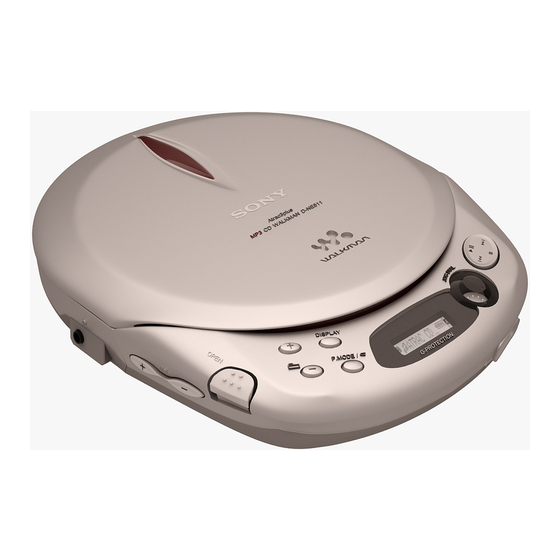
Advertisement

D-NE510/NE511/NE518CK
QQ
3 7 63 1515 0
SERVICE MANUAL
Ver. 1.1 2005.06
TE
L 13942296513
System
Compact disc digital audio system
Laser diode properties
Material: GaAlAs
Wavelength: λ = 780 nm
Emission duration: Continuous
Laser output: Less than 44.6 µW
(This output is the value measured at a distance
of 200 mm from the objective lens surface on
the optical pick-up block with 7 mm aperture.)
D-A conversion
1-bit quartz time-axis control
Frequency response
+1
20 – 20,000 Hz
dB
–2
(measured by JEITA CP-307)
Output (at 4.5 V input level)
Headphones (stereo minijack)
Approx. 5 mW + Approx. 5 mW at 16 Ω
(Approx. 1.5 mW + Approx. 1.5 mW
at 16 Ω)*
*For the customers in Europe
Power requirements
For the area code of the model you
purchased, check the upper left side of the
bar code on the package.
• Two LR6 (size AA) batteries: 1.5 V DC × 2
• AC power adaptor (DC IN 4.5 V jack):
US/CND/E92/MX model: 120 V, 60 Hz
AEP/EE model: 220 – 230 V, 50/60 Hz
UK model: 230 V, 50 Hz
AUS model: 240 V, 50 Hz
E18 model: 100 – 240 V, 50/60 Hz
www
.
Sony Corporation
9-877-188-02
2005F04-1
Personal Audio Group
© 2005.06
Published by Sony Engineering Corporation
http://www.xiaoyu163.com
Battery life*
(When you use the CD player on a flat and stable
surface)
Playing time varies depending on how the CD
player is used.
When using two Sony alkaline batteries
LR6 (SG) (produced in Japan)
Audio CD
ATRAC3plus files*
MP3 files*
*1 Measured value by the standard of JEITA
(Japan Electronics and Information Technology
Industries Association)
*2 When recorded at 48 kbps or 64 kbps
*3 When recorded at 128 kbps
Operating temperature
5°C – 35°C (41°F – 95°F)
Dimensions (w/h/d) (excluding
projecting parts and controls)
Approx. 136.0 × 26.3 × 156.3 mm
(5
Mass (excluding accessories)
Approx. 202 g (7.2 oz.)
Supplied accessories
D-NE510
Headphones (1) (US)
Earphones (1) (CND)
CD-ROM (SonicStage Simple Burner) (1)
User's guide for SonicStage Simple Burner (1)
x
ao
u163
y
i
http://www.xiaoyu163.com
2 9
8
Photo: D-NE518CK
Model Name Using Similar Mechanism
CD Mechanism Type
Optical Pick-up Name
SPECIFICATIONS
Q Q
3
6 7
1 3
1
(approx. hours)
G-PROTECTION function
"1"
"2"
50
45
2
80
80
3
75
75
× 1
× 6
in.)
3 ⁄8
1 ⁄16
1 ⁄4
.
9 4
2 8
US Model
Canadian Model
D-NE510/NE518CK
AEP Model
UK Model
Australian Model
D-NE511/NE518CK
1 5
0 5
8
2 9
9 4
D-NE511
AC power adaptor (1)
Earphones (1)
CD-ROM (SonicStage Simple Burner) (1)
User's guide for SonicStage Simple Burner (1)
D-NE518CK
AC power adaptor (1)
Headphones (1) (US)
Earphones (1) (Except US)
Rotary commander (RM-MC25C) (1)
Car battery cord (1)
Car connecting pack (1)
Velcro tapes for the CD player (2)
Velcro tape for the rotary commander (1)
CD-ROM (SonicStage Simple Burner) (1)
User's guide for SonicStage Simple Burner (1)
For US customers
The AC power adaptor supplied is not intended to
be serviced. Should the AC power adaptor cease to
function in its intended manner, during the warranty
period, the adaptor should be returned to your near-
est Sony Service Center or Sony Authorized Repair
Center for replacement, or after warranty period, it
should be discarded.
Design and specifications are subject to change
without notice.
• Abbreviation
CND : Canadian model
E18 : AC 100 – 240V area in E model
E92 : AC 120V area in E model
EE : East European model
AUS : Australian model
MX : Mexican model
m
PORTABLE CD PLAYER
co
9 9
E Model
NEW
CDM-3325ER2
DAX-25E
2 8
9 9
1

Advertisement

Table of Contents
loading

Summary of Contents for Sony D-NE510

  • Page 1 Power requirements est Sony Service Center or Sony Authorized Repair Approx. 136.0 × 26.3 × 156.3 mm For the area code of the model you Center for replacement, or after warranty period, it ×...
  • Page 2: Table Of Contents

    REPLACE THESE COMPONENTS WITH SONY PARTS WHOSE NE REMPLACER CES COMPOSANTS QUE PAR DES PIÈCES PART NUMBERS APPEAR AS SHOWN IN THIS MANUAL OR SONY DONT LES NUMÉROS SONT DONNÉS DANS CE MANUEL IN SUPPLEMENTS PUBLISHED BY SONY. OU DANS LES SUPPLÉMENTS PUBLIÉS PAR SONY.
  • Page 3: Service Note

    D-NE510/NE511/NE518CK SECTION 1 SERVICE NOTE 3 7 63 1515 0 NOTES ON HANDLING THE OPTICAL PICK-UP BLOCK detection lever OR BASE UNIT The laser diode in the optical pick-up block may suffer electro- static breakdown because of the potential difference generated by the charged electrostatic load, etc.
  • Page 4: General

    D-NE510/NE511/NE518CK SECTION 2 GENERAL 3 7 63 1515 0 This section is extracted from instruction manual. Getting started Locating the controls For details, see pages in parentheses. CD player (front) 1 i (headphones) 9 Display jack (pages 11, (pages 13, 16, 19 - 23)
  • Page 5: Disassembly

    D-NE510/NE511/NE518CK SECTION 3 DISASSEMBLY 3 7 63 1515 0 • The equipment can be removed using the following procedure. 3-1. LID (UPPER) ASSY (Page 5) 3-2. CABINET (FRONT) ASSY (Page 6) 3-3. MAIN BOARD (Page 6) Note : Follow the disassembly procedure in the numerical order given.
  • Page 6: Cabinet (Front) Assy

    D-NE510/NE511/NE518CK 3 7 63 1515 0 3-2. CABINET (FRONT) ASSY 4 screws (B 2) 3 screws (B 2) 2 screws (B 2) battery case lid 9 cabinet (front) assy 5 claw boss L 13942296513 6 claws 3-3. MAIN BOARD...
  • Page 7: Electrical Adjustments

    D-NE510/NE511/NE518CK SECTION 4 ELECTRICAL ADJUSTMENTS 3 7 63 1515 0 CD section adjustments are done automatically in this set. In case of operation check, confirm that focus bias. 4-1. FOCUS BIAS CHECK 1. Connect the oscilloscope between TJ601 (RF) and GND on main board.
  • Page 8: Diagrams

    D-NE510/NE511/NE518CK SECTION 5 DIAGRAMS 3 7 63 1515 0 5-1. IC PIN DESCRIPTIONS • IC601 CXD3048R (RF AMP, DIGITAL SIGNAL PROCESSOR, DIGITAL SERVO PROCESSOR, D-RAM CONTROLLER) Pin No. Pin Name Pin Description XRAS Low address strobe signal output to the D-RAM...
  • Page 9 D-NE510/NE511/NE518CK 3 7 63 1515 0 Pin No. Pin Name Pin Description TES1 Input terminal for the test (fixed at “L”) TEST Input terminal for the test (fixed at “L”) VSS1 — Ground LRMU Muting on/off control signal output to TA2120FN...
  • Page 10 D-NE510/NE511/NE518CK 3 7 63 1515 0 Pin No. Pin Name Pin Description PCMD_I Serial data input from CXR710 BCK_O Bit clock signal output to CXR710 BCK_I Bit clock signal input from CXR710 DVDD — Power supply 113 to 117...
  • Page 11 D-NE510/NE511/NE518CK 3 7 63 1515 0 • IC701 CXR710 (SOUND PROCESSOR) Pin No. Pin Name Pin Description LRCH D/A I/F L/R clock input from CXD3048 D/A I/F bit clock input from CXD3048 VDIOCD0 — Power supply (+2.0 V) PCMD...
  • Page 12 D-NE510/NE511/NE518CK 3 7 63 1515 0 Pin No. Pin Name Pin Description TEST3 Not used (pull down) TEST2 Not used (pull down) TEST1 Not used (pull down) DVDD3 — Power supply DVSS1 — Ground TEST0 Not used (pull down)
  • Page 13 D-NE510/NE511/NE518CK 3 7 63 1515 0 • IC801 TMP91CW28FG (SYSTEM CONTROL) Pin No. Pin Name Pin Description — Ground — Ground VCPU — Power supply (+2.0 V) XRST_O System reset signal output PWM_O Power on/off signal output (Not used)
  • Page 14 D-NE510/NE511/NE518CK 3 7 63 1515 0 Pin No. Pin Name Pin Description AT3_MP3_V_O IC701 reset P/S_O P/S signal output to LCD unit — Ground XNMI_I Not used (fixed at “H”) VCPU — Power supply (+2.0 V) HP_LIN_SEL_I HP/LINE select input (fixed at “H”)
  • Page 15: Block Diagram -Cd Section

    D-NE510/NE511/NE518CK 3 7 6 3 1 5 1 5 0 5-2. BLOCK DIAGRAM — CD SECTION — RF AMP, DIGITAL SIGNAL PROCESSOR, DIGITAL SERVO PROCESSOR, D-RAM CONTROLLER IC601 DETECTOR WDCK WFCK RFDC RFAC XTAO XTAI FOCUS/TRACKING COIL DRIVER, VCC1 SPINDLE/SLED MOTOR DRIVER (+2.2V)
  • Page 16: Block Diagram -Audio Section

    D-NE510/NE511/NE518CK 3 7 6 3 1 5 1 5 0 5-3. BLOCK DIAGRAM — AUDIO SECTION — 16 BIT D-RAM IC603 XRAS XCAS (Page 15) HEADPHONE AMP IC301 J301 LOUT VREF 7 ROUT MUTE MT SW NE518CK PWRSW PW SW...
  • Page 17: Block Diagram -Power Supply Section

    D-NE510/NE511/NE518CK 3 7 6 3 1 5 1 5 0 5-4. BLOCK DIAGRAM — POWER SUPPLY SECTION — POWER CONTROLLER IC403 (2/2) B+ +3V SWITCHING FOCUS/TRACKING COIL DRIVER VCC3 POWER SPINDLE/SLED MOTOR DRIVER (+2.6V) CIRCUIT 3 (IC403) +3V, HEADPHONE AMP...
  • Page 18: Printed Wiring Board -Main Section

    D-NE510/NE511/NE518CK 3 7 6 3 1 5 1 5 0 5-5. PRINTED WIRING BOARD — MAIN SECTION — Common Note on Schematic Diagram: • All capacitors are in µF unless otherwise noted. pF: µµF 50 WV or less are not indicated except for electrolytics and tantalums.
  • Page 19 D-NE510/NE511/NE518CK 3 7 6 3 1 5 1 5 0 • Refer to page 18 for Common note on Printed Wiring Board. • Semiconductor MAIN BOARD (SIDE B) Location (Side B) Ref. No. Location D303 D304 D305 R713 D308...
  • Page 20: Schematic Diagram -Main Section (1/2)

    D-NE510/NE511/NE518CK 3 7 6 3 1 5 1 5 0 5-6. SCHEMATIC DIAGRAM — MAIN SECTION (1/2) — • Refer to page 22 for IC Block Diagram. • Refer to page 18 for Common Note on Schematic Diagram. IC B/D...
  • Page 21: Schematic Diagram -Main Section (2/2)

    D-NE510/NE511/NE518CK 3 7 6 3 1 5 1 5 0 5-7. SCHEMATIC DIAGRAM — MAIN SECTION (2/2) — • Refer to page 22 for IC Block Diagram. • Refer to page 18 for Common Note on Schematic Diagram. (Page 20)
  • Page 22: Ic Block Diagrams

    D-NE510/NE511/NE518CK 3 7 6 3 1 5 1 5 0 5-8. IC BLOCK DIAGRAMS IC301 TA2120FN IC403 TB2138FG 60 59 58 57 56 BEEP BIAS VREF H BRIDGE H BRIDGE H BRIDGE ROUT LOUT 40 LATCH DCIN DC IN...
  • Page 23: Exploded Views

    D-NE510/NE511/NE518CK SECTION 6 EXPLODED VIEWS 3 7 63 1515 0 NOTE: • The mechanical parts with no reference The components identified by • Color Indication of Appearance Parts mark 0 or dotted line with mark number in the exploded views are not supplied.
  • Page 24: Main Board Section

    D-NE510/NE511/NE518CK 3 7 63 1515 0 6-2. MAIN BOARD SECTION CDM-3325ER2 LCD801 L 13942296513 Ref. No. Part No. Description Remark Ref. No. Part No. Description Remark 3-245-331-01 INSULATOR 3-249-876-01 BOARD (–), TERMINAL, BATTERY 3-245-557-01 TERMINAL, BATTERY LINK 3-249-875-01 BOARD (+), TERMINAL, BATTERY...
  • Page 25: Cd Mechanism Deck Section (Cdm-3325Er2)

    D-NE510/NE511/NE518CK 3 7 63 1515 0 6-3. CD MECHANISM DECK SECTION (CDM-3325ER2) M502 M501 L 13942296513 The components identified by Les composants identifiés par une mark 0 or dotted line with mark marque 0 sont critiques pour 0 are critical for safety.
  • Page 26: Q Q 7. Electrical Parts List

    D-NE510/NE511/NE518CK SECTION 7 MAIN ELECTRICAL PARTS LIST 3 7 63 1515 0 NOTE: • Due to standardization, replacements in • SEMICONDUCTORS The components identified by mark 0 or dotted line with mark the parts list may be different from the In each case, u : µ, for example:...
  • Page 27 D-NE510/NE511/NE518CK MAIN 3 7 63 1515 0 Ref. No. Part No. Description Remark Ref. No. Part No. Description Remark C631 1-119-750-11 TANTAL. CHIP 22uF 6.3V D422 8-719-404-50 DIODE MA111-TX C632 1-164-156-11 CERAMIC CHIP 0.1uF D425 8-719-083-04 DIODE RSB6.8STE61 C696...
  • Page 28 D-NE510/NE511/NE518CK MAIN 3 7 63 1515 0 Ref. No. Part No. Description Remark Ref. No. Part No. Description Remark L407 1-456-178-21 COIL, CHOKE 100uH R456 1-216-864-11 METAL CHIP 1/10W L408 1-400-388-11 INDUCTOR 220uH R459 1-216-845-11 METAL CHIP 100K 1/10W...
  • Page 29 D-NE510/NE511/NE518CK Ver. 1.1 MAIN 3 7 63 1515 0 Ref. No. Part No. Description Remark Ref. No. Part No. Description Remark R714 1-216-864-11 METAL CHIP 1/10W R877 1-216-845-11 METAL CHIP 100K 1/10W R715 1-216-864-11 METAL CHIP 1/10W R886 1-216-845-11 METAL CHIP...
  • Page 30 D-NE510/NE511/NE518CK Ver. 1.1 MAIN 3 7 63 1515 0 Ref. No. Part No. Description Remark Ref. No. Part No. Description Remark S811 1-553-977-00 SWITCH, SLIDE (G-PROTECTION) ACCESSORIES S812 1-786-442-11 SWITCH, TACT (x) ************ S813 1-692-014-11 SWITCH, KEYBOARD (P.MODE/ S814...
  • Page 31 D-NE510/NE511/NE518CK 3 7 63 1515 0 MEMO L 13942296513 u163 http://www.xiaoyu163.com...
  • Page 32 D-NE510/NE511/NE518CK 3 7 63 1515 0 REVISION HISTORY Clicking the version allows you to jump to the revised page. Also, clicking the version at the upper on the revised page allows you to jump to the next revised page.

This manual is also suitable for:

D-ne511D-ne518ck

Table of Contents