Table of Contents
Advertisement
Advertisement
Table of Contents

Related Manuals for Harman Kardon AVR-134


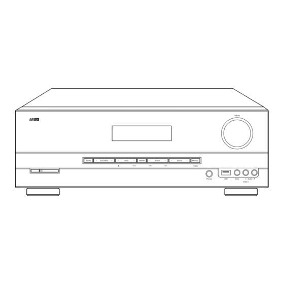
Summary of Contents for Harman Kardon AVR-134
-
Page 2: Safety Precautions
SAFETY PRECAUTIONS WARNING Before servicing this unit, familiarize yourself with the following precautions: 1. Many electrical and mechanical parts in this exposed metal parts of the cabinet, such as chassis have special safety characteristics that terminals, screw heads, and metal overlays, to often pass unnoticed and the protection be sure the set is safe to operate danger of afforded by them cannot necessarily be... - Page 3 SPECIFICATION Measuring methods are based on IHF and IEC standard 268-3 Measurements conditions,unless otherwise noted : Output resistive load = (6) ohms / Both channel driven Tone Direct ON , Other SW's : OFF Power figures should be kept minimum 10min. between 15 and 35˚c Filter : IHF-A filter, R/O = Rated Output Power supply : 240 V / 50 Hz...
- Page 4 3. SURROUND AMP SECTION *SPKR LEVEL : ALL 0dB *SPK SIZE:LLLY *6CH INPUT *TONE OFF DESCRIPTION INPUT FREQ. REMARK UNIT NOMINAL LIMIT INPUT SENSITIVITY 6CH INPUT 1kHz 200±30 200±50 TOTAL HARMONIC DISTORTION 6CH INPUT 20Hz R/O-3dB 0.07 0.09 (STEREO IN) 1kHz R/O-3dB 0.07...
- Page 5 6. Idle Voltage *6CH Input *Main Vol : -18dB *SPK SIZE:LLLY *TEST B'D : AMP *TONE OFF(TONE DIRECT), *SPKR LEVEL : ALL 0dB *Test Point : R221(FL,FR,SL,SR,C) Both Sides Voltage(DC). CHANNEL INPUT FREQ. REMARK UNIT NOMINAL LIMIT R221FL 2.7±0.3 2.7±0.5 R221FR 2.7±0.3 2.7±0.5...
- Page 6 8. DTS INPUT SECTION INPUT : COAXIAL, CD DIGITAL VOLUME POSISTION : -18dB SURROUND MODE : DTS SURROUND AT PREOUT SPK MODE LLLY DTS TEST Disc(TRACK 9,10,11,12,13,14,15) DESCRIPTION INPUT FREQ. TRACK UNIT NOMINAL LIMIT OUTPUT LEVEL FRONT 10,11 9.5±1 9.5±2 1kHz Disc : DTS 0dB CENTER...
- Page 7 9. FM SECTION Measuring methods in confirmity with IEC standard 315 Measurements condition FM : Ref. frequency = ( 98.1 MHz), Audio frequency = 1kHz Reference level = 1 mV on (75ohms, 300ohms) Deviation : Filter = B.P.F at STEREO and MONO Test Point : TP1 = 90.1 MHz, TP2 = 98.1 MHz, TP3 = 106.1 MHz (50kHz STEP) MOD:40 kHz (Mono)/40 kHz±7.5 kHz (STEREO) DESCRIPTION...
- Page 8 10. AM SECTION Measurements condition AM - MW : Radio. frequency = 1000/999 kHz , Audio frequency = 400 Reference level = (74dBu/m),(50)ohms Modulation = ( 30 )% Test Point : MW TP 1 = (594/600) kHz , TP 2 = (999/1000) kHz , TP 3 = (1404/1400) kHz DESCRIPTION UNIT NOMI.
- Page 9 CIRCUIT DESCRIPTION UPD78F0536GK : IC101 1. Pin Description...
- Page 10 2. Block Diagram TO00/TI010/P01 16-bit TIMER/ TI000/P00 (LINSEL) EVENT COUNTER 00 PORT 0 P00 to P06 RxD6/P14 (LINSEL) Note 2 Note 2 16-bit TIMER/ TO01 /TI011 /P06 PORT 1 P10 to P17 Note2 Note 2 EVENT COUNTER 01 TI001 /P05 PORT 2 P20 to P27 TOH0/P15...
- Page 11 3. Pin Functions Pin Name Pin Symbol Pin Description P120/INTP0/EXLVI PROTECTION Input for protection VOL_UP Input for volume up VOL_DN Input for volume down H/P_RLY Output for headphone relay C_RLY Output for center speaker relay RESET RESET Input for u-com reset P124/XT2/EXCLKS S_RLY Output for surround speaker relay...
- Page 12 Pin Name Pin Symbol Pin Description DSP_RDY Input for DSP enable P30/INTP1 DSP_CE Chip select output for NJW1153 P17/TI50/TO05 DSP_ABOOT Ouput for DSP Auto boot P16/TOH1/INTP5 DSP_INTREQ Interrupt signal output to DSP P15/TOH0 DIR_PDN Output for DIR power down P14/RXD6 Input for flash upgrade P13/TXD6 Output for flash upgrade...
-
Page 14: Block Diagram
2. Block Diagram Program/Data JTAG EMU 192K Bytes McASP0 Data 16 Serializers Program/Data C67x+ CPU ROM Page1 256K Bytes Memory Data Controller Program/Data McASP1 ROM Page2 6 Serializers 256K Bytes Program Fetch Program/Data McASP2 ROM Page3 2 Serializers 256K Bytes DIT Only Program SPI1... - Page 15 3. Terminal Functions Table, the Terminal Functions table, identifies the external signal names, the associated pin/ball numbers along with the mechanical package designator, the pin type(I,O, IO, OZ, or PWR), whetherthe pin/ball has any internal pullup/pulldown resistors, whether the pin/ball is configurable as an IO in GPIO mode, and a functional pin description.
- Page 16 SIGNAL NAME TYPE PULL GPIO DESCRIPTION McASP0, McASP1, McASP2, and SPI1 Serial Ports AHCLKR0/AHCLKR1 McASP0 and McASP1 ReceiveMasterClock ACLKR0 McASP0 ReceiveBit Clock AFSR0 McASP0 ReceiveFrameSync(L/RClock) AHCLKX0/AHCLKX2 McASP0 and McASP2 Transmit MasterClock ACLKX0 McASP0 Transmit Bit Clock AFSX0 McASP0 TransmitFrame Sync(L/RClock) AMUTE0 McASP0 MUTE Output AXR0[0]...
- Page 17 SIGNAL NAME TYPE PULL GPIO DESCRIPTION Emulation/JTAG Port Test Clock Test Mode Select Test DataIn Test DataOut Test Reset TRST EmulationPin 0 EMU[0] EmulationPin 1 EMU[1] Power Pins Core Supply(CV 8, 16,20,33,44,53,57,65,77,85,90,101,123,128,132 IO Supply(DV 10,31,42,50,60,68,73,81,92,103,112,125,136 Ground(V 1, 6, 13,15,18,26,30,36,40,47,54,62,69,72,78,82,87,95,99,106,109,114,118,124,129, 133,140 (1) TYPE column refers to pin direction in functional mode.
- Page 18 AK4588 : IC103 TE S T 1 INT1 RX 1 BOUT TV DD RX 0 DVDD AVS S DVSS AVDD VREF H XT I VCOM TE S T 3 RI N MCKO 2 LI N (Top View ) MCKO 1 CO UT RO UT1 UOUT...
- Page 19 Pin Name Function IN T1 Interrupt 1 Pin Bl oc k-Start Ou tput Pi n for Re ceiv er Input BO UT ìH î durin g fi rst 40 flam es. T VDD Output Bu ffer Po we r Supply Pin, 2.7V ~5.5V DV DD Di gital Power Supply Pin, 4.5V ~5.5V DV SS...
- Page 20 No . Pin Name Function No Co nnect pin No internal bonding . Th is pin should be opened. RO UT 3 DA C3 Rc h An alog Ou tput Pi n No Co nnect pin No internal bonding . Th is pin should be opened. LO UT 2 AC 2 Lc h An alog Ou tput Pin No Co nnect pin...
-
Page 21: Alignment Procedures
ALIGNMENT PROCEDURES 1.Electrical specification. SPECIFICATION ITEMS Above the receiving Frequency Local OSC 522 ~1620kHz 87.5 ~ 108.0MHz Frequency cover range 12.0(±0.5V) Standard supply voltage 75 ohm FM Antenna input Impedance 9.5uH ( 1kHz ) : S0160BL-25 AM Loop Antenna 2.Electrical Characteristics. T.L. -
Page 22: Troubleshooting
TROUBLESHOOTING Symptom Cause and Remedy Ref No. Power On Failure A) ACCord check. 1. FLT does not light up. B) PowerTrans (Main/Standby) check. 2. STANDBY LED does not light C) Fuse’s disconnection check. F (301) D) Connector’s disconnection or disjuction. Change or close insertion of the connector. - Page 23 Symptom Cause and Remedy Ref No. Sounds from Speaker when A) NOT Supported Headphone Detect. Headphone’s connected. Push the Speaker On/Off Button (Speaker off). Bass / Treble Control Failure. A) Volume IC check. I.C 109 1. Resistor/Capacitor correction figure check. I.C 109 PIN No.(26, 27, 32, 33) (Bass) I.C 109 PIN No.(28, 34)
- Page 24 Symptom Cause and Remedy Ref No. FM Failure. A) FM Mute adjustment inferior. B) FRONTEND inferior. C) FM DET COIL inferior. D) PLL & MPX IC check. 1. PLL & MPX I.C B+(5)V, B+(3.3)V check. I.C NO. (1) / I.C Pin No. (8, 21) 2.
- Page 25 BLOCK DIAGRAM Model : AVR-134...
- Page 26 WIRING DIAGRAM Model : AVR-134...
-
Page 27: Mechanical Parts List
MECHANICAL PARTS LIST Model : AVR-134 Parts without Parts No. are not supplied. Parts without version mentioned are common ones. DESCRIPTION Q'TY PARTS NO. VER. DESCRIPTION Q'TY PARTS NO. VER. DESCRIPTION Q'TY PARTS NO. VER. PACKAGE MISCELLANEOUS SW,ENCODER G121123070020S INSTRUCTION MANUAL... - Page 28 EXPLODED VIEW Model : AVR-134...
-
Page 29: Electrical Parts List
ELECTRICAL PARTS LIST Model : AVR-134 Parts without Parts No. are not supplied. Parts without version mentioned are common ones. DESCRIPTION PART NO. DESCRIPTION PART NO. DESCRIPTION PART NO. REF NO. Q'TY REF NO. Q'TY REF NO. Q'TY P.C.B TOTAL ASSY... - Page 30 REF NO. DESCRIPTION Q'TY PART NO. REF NO. DESCRIPTION Q'TY PART NO. REF NO. DESCRIPTION Q'TY PART NO. IC107 IC,MEMORY-EEPROM FT24C08 J000240800020S R123 R,CHIP THICK 4.7 kohm 1/16W C20004726M160S R190 R,METAL FILM 100PPM 47 kohm 1/4W C060047363050S IC108 IC,LINEAR-REGULATOR KIA78R05PI J126780500370S R124/R125 R,CARBON FILM...
- Page 31 REF NO. DESCRIPTION Q'TY PART NO. REF NO. DESCRIPTION Q'TY PART NO. REF NO. DESCRIPTION Q'TY PART NO. MISCELLANEOUS COMPONENT-MANUAL P.C.B INS ASSY 7027067685M10 D201C/FL/FR/SL/SR D,SWITCHING 1SS133T K000013300520S GND101 TERMINAL 3790040886000S P.C.B INS ASSY COMPONENT-RADIAL 7027067685R10 J204/J206/J208 CN,WIRE 1P 0.6/52MM L045084006040S GND102 TERMINAL...
- Page 32 REF NO. DESCRIPTION Q'TY PART NO. REF NO. DESCRIPTION Q'TY PART NO. REF NO. DESCRIPTION Q'TY PART NO. FRONT P.C.B TOTAL ASSY 7025HK0814012 R749/R751 R,CHIP THICK 2.2 kohm 1/16W C20002226M160S P.C.B TOTAL ASSY 7025HK0814013 FRONT P.C.B SUB ASSY 7028066851010 R752/R754 R,CHIP THICK 1.5 kohm 1/16W...
- Page 33 REF NO. DESCRIPTION Q'TY PART NO. REF NO. DESCRIPTION Q'TY PART NO. REF NO. DESCRIPTION Q'TY PART NO. IC102 IC,ANALOG TMS320DA787 J080320787010S R216 R,CHIP THICK 0 ohm 1/16W C20000006M160S D302-D304 D,SWITCHING CHIP 1N4148WS K005041483230S IC103 IC,ANALOG AK4588 J080458800010S R217/R218 R,CHIP THICK 10 kohm 1/16W C20001036M160S...
- Page 34 REF NO. DESCRIPTION Q'TY PART NO. R27/R28 R,CHIP THICK 4.7 kohm 1/16W C20004726M160S R09/R10 R,CHIP THICK 4.7 kohm 1/16W C20004736M160S R107 R,CHIP THICK 4.7 kohm 1/16W C20004736M160S R11/R12 R,CHIP THICK 4.7 kohm 1/16W C20004736M160S R43/R44 R,CHIP THICK 4.7 kohm 1/16W C20004736M160S C21/C23 C,CERAMIC CHIP T.C...
- Page 35 PRINTED CIRCUIT BOARDS_1 Model : AVR-134 MAIN-TOP...
- Page 36 PRINTED CIRCUIT BOARDS_2 Model : AVR-134 MAIN-BOTTOM...
- Page 37 PRINTED CIRCUIT BOARDS_3 Model : AVR-134 FRONT-TOP PRINTED CIRCUIT BOARDS_4 FRONT-BOTTOM...
- Page 38 PRINTED CIRCUIT BOARDS_5 Model : AVR-134...
- Page 39 PRINTED CIRCUIT BOARDS_6 Model : AVR-134 DSP-TOP PRINTED CIRCUIT BOARDS_7 DSP-BOTTOM...
- Page 40 PRINTED CIRCUIT BOARDS_8 Model : AVR-134 HDMI-TOP PRINTED CIRCUIT BOARDS_9 HDMI-BOTTOM...
- Page 41 PRINTED CIRCUIT BOARDS_10 PRINTED CIRCUIT BOARDS_11 STANDBYI-TOP 1STANDBY-BOTTOM Model : AVR-134...
- Page 42 SCHEMATIC DIAGRAMS_1 Model : AVR-134 MAIN_1...
- Page 43 SCHEMATIC DIAGRAMS_2 Model : AVR-134 MAIN_2...
- Page 44 SCHEMATIC DIAGRAMS_3 Model : AVR-134 COMPONENT...
- Page 45 SCHEMATIC DIAGRAMS_4 Model : AVR-134 FRONT...
- Page 46 SCHEMATIC DIAGRAMS_5 Model : AVR-134...
- Page 47 SCHEMATIC DIAGRAMS_6 Model : AVR-134 DSP_DA787...
- Page 48 SCHEMATIC DIAGRAMS_7 Model : AVR-134 DSP-DIR WITH CODEC...
- Page 49 SCHEMATIC DIAGRAMS_8 Model : AVR-134 DSP-UBI9022...
- Page 50 SCHEMATIC DIAGRAMS_9 Model : AVR-134 STANDBY...
- Page 51 SCHEMATIC DIAGRAMS_10 Model : AVR-134 TUNER ASS’Y...
- Page 52 SCHEMATIC DIAGRAMS_11 Model : AVR-134 HDMI...