Table of Contents
Advertisement
Quick Links
SERVICE MANUAL
Ver 1.0 2001.06
US and foreign patents licensed from Dolby
Laboratories.
System
Disc
Laser
Laser output
1)
This output is the value measured at a distance of
200 mm from the objective lens surface on the
Optical Pick-up Block with 7 mm aperture.
Laser diode
Revolutions (CLV)
Error correction
Sampling frequency
Coding
Modulation system
Number of channels
Frequency response
Signal-to-noise ratio
Wow and flutter
Inputs
ANALOG IN
DIGITAL IN
Sony Corporation
9-873-914-11
2001F0500-1
Home Audio Company
C 2001.6
Shinagawa Tec Service Manual Production Group
SPECIFICATIONS
Outputs
MiniDisc digital audio
system
ANALOG OUT
MiniDisc
Semiconductor laser ( λ =
780 nm) Emission
duration: continuous
MAX 44.6 µW
1)
General
Power requirements
Power consumption
Material: GaAlAs
400 rpm to 900 rpm
ACIRC (Advanced Cross
Dimensions (approx.)
Interleave Reed Solomon
Code)
44.1 kHz
Mass (approx.)
ATRAC (Adaptive
Supplied accessories
TRansform Acoustic
Coding)/ATRAC 3
Audio connecting cords (2)
EFM (Eight-to-Fourteen
Optical cable (1)
Modulation)
Remote commander (remote) (1)
2 stereo channels
R6 (size-AA) batteries (2)
5 to 20,000 Hz ±0.3 dB
Over 96 dB during play
Design and specifications are subject to change
Below measurable limit
without notice.
Jack type: phono
Impedance: 47 kilohms
Rated input: 500 mVrms
Minimum input:
125 mVrms
Connector type: square
optical
Impedance: 660 nm
(optical wave length)
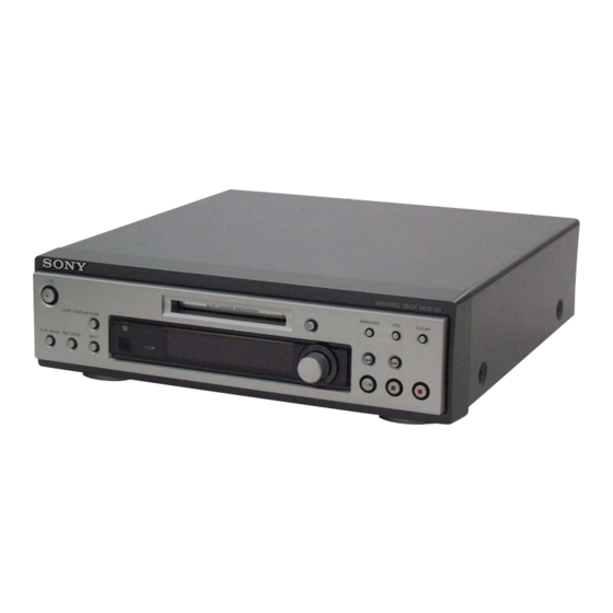
MDS-S9
Model Name Using Similar Mechanism
MD Mechanism Type
Optical Pick-up Name
Jack type: phono
Rated output: 2 Vrms (at
50 kilohms)
Load impedance: over 10
kilohms
230 V AC, 50/60Hz
15 W
0.5 W (at the STANDBY
mode)
280 × 83 × 290 mm (w/
h/d) incl. projecting parts
and controls
2.4 kg
MINIDISC DECK
AEP Model
UK Model
MDS-S50
MDM-7A
KMS-260B
Advertisement
Table of Contents

Related Manuals for Sony MDS-S9


Summary of Contents for Sony MDS-S9
- Page 1 MDS-S9 SERVICE MANUAL AEP Model UK Model Ver 1.0 2001.06 US and foreign patents licensed from Dolby Model Name Using Similar Mechanism MDS-S50 Laboratories. MD Mechanism Type MDM-7A Optical Pick-up Name KMS-260B SPECIFICATIONS Outputs System MiniDisc digital audio system ANALOG OUT...
-
Page 2: Self-Diagnosis Function
If the code and message alternate, find them in the following table and perform the indicated countermeasure. Should the problem persist, consult your nearest Sony dealer. C11/Protected , Take out the MD and close the record-protect slot. - Page 3 MDS-S9 ITEMS OF ERROR HISTORY MODE ITEMS AND CONTENTS Display Details of History op rec tm Cumulative recording time is displayed. When cumulative recording time is over 1 minute, the hour and minute are displayed as they are. When it is under 1 minute, “Under 1 min” is displayed.
- Page 4 MDS-S9 Table of Error Codes Error Code Details of Error Loading failed Loading switch combination is illegal Head of PTOC could not be read within the specified time Head of PTOC could be read but its content is erroneous Access to UTOC could not be made within the...
-
Page 5: Table Of Contents
• Do not touch the soldering iron on the same conductor of the OPERATION. REPLACE THESE COMPONENTS WITH circuit board (within 3 times). SONY PARTS WHOSE PART NUMBERS APPEAR AS • Be careful not to apply force on the conductor when soldering SHOWN IN THIS MANUAL OR IN SUPPLEMENTS PUB- or unsoldering. -
Page 6: Servicing Notes
MDS-S9 SECTION 1 SERVICING NOTES NOTES ON LASER DIODE EMISSION CHECK NOTES ON HANDLING THE OPTICAL PICK-UP Never look into the laser diode emission from right above when BLOCK OR BASE UNIT checking it for adjustment. It is feared that you will lose your sight. - Page 7 MDS-S9 IOP DATA RECORDING AND DISPLAY WHEN OPTICAL PICK-UP AND NON-VOLATILE MEMORY (IC195 OF BD BOARD) ARE REPLACED The IOP value labeled on the optical pick-up can be recorded in the non-volatile memory. By recording the value, it will eliminate the need to look at the value on the label of the optical pick-up.
- Page 8 MDS-S9 RETRY CAUSE DISPLAY MODE IN MD • In this test mode, the causes for retry of the unit during recording and stop can be displayed on the liquid crystal display. During playback, the “track mode” for obtaining track information will be set.
- Page 9 MDS-S9 Reading the Retry Cause Display Higher Bits Lower Bits Hexa- Details Hexadecimal decimal When 0 When 1 b7 b6 b5 b4 b3 b2 b1 b0 Binary Emphasis OFF Emphasis ON Monaural Stereo This is 2-bit display. Normally 01. 01: Normal audio. Others: Invalid...
-
Page 10: General
MDS-S9 SECTION 2 This section is extracted from instruction manual. GENERAL LOCATION OF CONTROLS – Front Panel – AMS qd (8) (10) (12) (13) (16) PLAY MODE qk (16) BUTTON DESCRIPTIONS REC MODE qj (9) (24) CLEAR 8 (7) (16) (18) (24) -
Page 11: Remote Control
MDS-S9 Remote control AyB qs (16) CD PLAYER . (go back)/> (go forward) ql (15) CD-SYNCHRO STANDBY/START/STOP 7 (14) (15) CLEAR 6 (16) (18) (24) DISPLAY ws (8) (12) FADER 3 (28) INPUT wf (8) Letter/number buttons 5 (17) (25) LEVEL +/–... -
Page 12: Disassembly
MDS-S9 SECTION 3 DISASSEMBLY • This set can be disassembled in the order shown below. 3-1. DISASSEMBLY FLOW 3-2. CASE (Page 13) 3-3. MD MECHANISM DECK (MDM-7A) (Page 13) 3-4. MAIN BOARD 3-5. BD BOARD (Page 14) (Page 14) -
Page 13: Case
MDS-S9 Note: Follow the disassembly procedure in the numerical order given. 3-2. CASE 2 case 1 two screws (case 3 TP2) 1 two screws (case 3 TP2) 3-3. MD MECHANISM DECK (MDM-7A) 3 four screws (BVTTWH M3) 1 wire (flat type) (23 core) -
Page 14: Main Board
MDS-S9 3-4. MAIN BOARD 2 connector (CN902) 1 wire (flat type) (15 core) (CN490) 4 two screws (BVTP3 × 8) 5 MAIN board 3 three screws (BVTP3 × 8) 3-5. BD BOARD BD board – CONDUCTOR SIDE VIEW – 5 Remove four solders. -
Page 15: Test Mode
MDS-S9 SECTION 4 TEST MODE 4-1. PRECAUTIONS FOR USE OF TEST MODE • As loading related operations will be performed regardless of the test mode operations being performed, be sure to check that the disc is stopped before setting and removing it. -
Page 16: Selecting The Test Mode
MDS-S9 4-5. SELECTING THE TEST MODE There are 26 types of test modes as shown below. The groups can be switched by turning the knob. After selecting the > [YES] group to be used, press the button. After setting a certain group, turning the >... - Page 17 MDS-S9 4-5-1. Operating the Continuous Playback Mode 1. Entering the continuous playback mode (1) Set the disc in the unit. (Whichever recordable discs or discs for playback only are available) (2) Turn the > knob to display “CPLAY1MODE” (C34). [YES] (3) Press the button to change the display to “CPLAY1MID”.
- Page 18 MDS-S9 4-7. TEST MODE DISPLAYS [LEVEL/DISPLAY/CHAR] Each time the button is pressed, the display changes in the following order. When CPLAY or CREC are started, the display will forcibly be switched to the error rate display as the initial mode.
- Page 19 MDS-S9 4-8. AUTOMATIC SELF-DIAGNOSIS FUNCTION This test mode performs CREC and CPLAY automatically for mainly checking the characteristics of the optical pick-up. To perform this test mode, the laser power must first be checked. Perform AUTO CHECK after the laser power check and Iop Compare.
-
Page 20: Electrical Adjustments
MDS-S9 SECTION 5 ELECTRICAL ADJUSTMENTS 5-1. PARTS REPLACEMENT AND ADJUSTMENTS If malfunctions caused by optical pick-up such as sound skipping are suspected, follow the following check. Check before replacement Start 5-7-2. Laser Power Check (See page 23) 5-7-3. Iop Compare (See page 23) 5-7-4. - Page 21 MDS-S9 Adjustment flow • Abbreviation Start OP: optical pick-up After turning off and then on the power, initialize the EEPROM Replace IC195 For details, refer to “WHEN MEMORY NG IS DIS- PLAYED” in 1. SERVICING NOTES (See page 7) 5-8. INITIAL SETTING OF ADJUSTMENT VALUE...
- Page 22 MDS-S9 5-2. PRECAUTIONS FOR CHECKING LASER 5-4. HOW TO DISTINGUISH BETWEEN OPTICAL DIODE EMISSION PICK-UP KMS-260B AND KMS-260E To check the emission of the laser diode during adjustments, never Two types of optical pick-up, KMS-260B and KMS-260E, are used view directly from the top as this may lose your eye-sight.
- Page 23 MDS-S9 5-6. USING THE CONTINUOUSLY RECORDED Procedure: 1. Set the laser power meter on the objective lens of the opti- DISC • This disc is used in focus bias adjustment and error rate check. cal pick-up. (When it cannot be set properly, press button or button to move the optical pick-up.)
- Page 24 MDS-S9 5-7-6. Traverse Check 5-7-4. Auto Check This test mode performs CREC and CPLAY automatically for mainly checking the characteristics of the optical pick-up. To Note 1:Data will be erased during MO reading if a recorded disc is used in this adjustment.
- Page 25 MDS-S9 [YES] 9. Press the button to display “EFB = MO-P”. 5-7-7. Focus Bias Check Then, the optical pick-up moves to the pit area automatically Change the focus bias and check the focus tolerance amount. and servo is imposed. Procedure: 10.
- Page 26 MDS-S9 5-8. INITIAL SETTING OF ADJUSTMENT VALUE 5-10. TEMPERATURE COMPENSATION OFFSET ADJUSTMENT Note: Save the temperature data at that time in the non-volatile memory Mode which sets the adjustment results recorded in the non-volatile as 25 ˚C reference data. memory to the initial setting value. However the results of the tempera-...
- Page 27 MDS-S9 6. Turn the knob so that the reading of the laser 4. After “Complete!” is displayed momentarily, the display changes > [YES] power meter becomes 6.9 to 7.1 mW, press the button to “Iop 7.0mW”. [YES] to save it. (“LD SAVE $ ”...
- Page 28 MDS-S9 [YES] 8. Turn the knob so that the waveform of the 18. Press the button, display “EFB = SAVE” for a mo- > oscilloscope becomes the specified value. ment and save the adjustment results in the non-volatile (When the >...
- Page 29 MDS-S9 5-15. ERROR RATE CHECK 5-17. AUTO GAIN CONTROL OUTPUT LEVEL ADJUSTMENT 5-15-1. CD Error Rate Check Be sure to perform this adjustment when the optical pick-up is Procedure: replaced. 1. Load the check disc (TDYS-1). If the adjustment results becomes “Adjust NG!”, the optical pick- 2.
- Page 30 MDS-S9 Adjustment and checking Loacation: – BD BOARD (Component Side) – D101 CN101 – BD BOARD (Conductor Side) – IC101 CN105 1. I+3V 2. IOP 3. GND 4. TE 5. FE 6. VC 7. RF IC151 IC190 Note: It is useful to use the jig for checking BD board waveform. (Refer...
-
Page 31: Diagrams
MDS-S9 SECTION 6 DIAGRAMS DIGITAL SIGNAL PROCESSOR, EFM/ACIRC ENCODER/DECODER, 6-1. BLOCK DIAGRAM – SERVO Section – SHOCK PROOF MEMORY CONTROLLER, ATRAC ENCODER/DECODER IC151 (1/2) (Page 32) IC151 (1/2) OVER WRITE EFMO ADDT ADDT HEAD DRIVE IC181, Q181, 182 SAMPLING DATAI... -
Page 32: Block Diagram - Main Section
MDS-S9 6-2. BLOCK DIAGRAM – MAIN Section – A/D, D/A CONVERTER IC500 J150 • SIGNAL PATH AINL HIGH-PASS FILTER, LINE ADDT SDTO SUB- : PLAY (ANALOG OUT) ANALOG DIGITAL CONVERTER TRACKTION AINR ATTENUATOR BLOCK IC350 : REC (ANALOG IN) (Page 31) -
Page 33: Note For Printed Wiring Boards And Schematic Diagrams
MDS-S9 6-3. NOTE FOR PRINTED WIRING BOARDS AND SCHEMATIC DIAGRAMS • IC Block Diagrams – BD Board – Note on Printed Wiring Board: Note on Schematic Diagram: • All capacitors are in µF unless otherwise noted. pF: µµF • X : parts extracted from the component side. - Page 34 MDS-S9 IC141 BH6519FS-E2 – MAIN Board – IC400 LA5643 IC440 LB1641 T.S.D O.C.P – MOTOR MOTOR INTERFACE INTERFACE DRIVE DRIVE STBY CHARGE PREDRIVE PREDRIVE ANA5 PUMP. – FWD/REV/STOP PREDRIVE PREDRIVE SYS3.3 CONTROL LOGIC – INTERFACE INTERFACE – 3.3V B.BAK IC480 M5293L –...
-
Page 35: Printed Wiring Boards - Bd Board
MDS-S9 6-4. PRINTED WIRING BOARDS – BD Board – BD BOARD FLEXIBLE BOARD BD BOARD (CONDUCTOR SIDE) (COMPONENT SIDE) S102-2 PROTECT (LOADING) –2 DETECT –1 S102-1 REFLECT RATE DETECT (PACK OUT) TEST PLAY POSITION POSITION (SLED) (22) (22) MAIN BOARD... -
Page 36: Schematic Diagram - Bd Board (1/2)
MDS-S9 6-5. SCHEMATIC DIAGRAM – BD Board (1/2) – • • See page 43 for Waveforms. See page 33 for IC Block Diagrams. (Page (Page (Page The components identified by mark 0 or dotted line with mark 0 are critical for safety. -
Page 37: Schematic Diagram - Bd Board (2/2)
MDS-S9 6-6. SCHEMATIC DIAGRAM – BD Board (2/2) – • • See page 43 for Waveforms. See page 33 for IC Block Diagram. (Page 36) (Page 40) (Page 36) (Page 41) (Page 36) -
Page 38: Printed Wiring Board - Main Board (Component Side)
MDS-S9 6-7. PRINTED WIRING BOARD – MAIN Board (Component Side) – • Semiconductor Location Ref. No. Location (Page 44) D155 DISPLAY BOARD D156 CN701 MAIN BOARD D255 (COMPONENT SIDE) D256 D401 D402 D403 D404 D412 D421 D422 D431 D432 D482... -
Page 39: Printed Wiring Board - Main Board (Conductor Side)
MDS-S9 6-8. PRINTED WIRING BOARD – MAIN Board (Conductor Side) – • Semiconductor Location Ref. No. Location D461 SHORT ANALOG D462 SOCKET IC611 J800 D471 MAIN BOARD OPTICAL IN PC LINK D472 D476 (CONDUCTOR SIDE) D477 D481 IC400 IC440 IC480... -
Page 40: Schematic Diagram - Main Board (1/3)
MDS-S9 6-9. SCHEMATIC DIAGRAM – MAIN Board (1/3) – • See page 43 for Waveform. (Page (Page 37) (Page (Page 42) (Page 45) -
Page 41: Schematic Diagram - Main Board (2/3)
MDS-S9 6-10. SCHEMATIC DIAGRAM – MAIN Board (2/3) – • • See page 43 for Waveforms. See page 33 for IC Block Diagram. (Page 37) (Page 40) (Page 42) -
Page 42: Schematic Diagram - Main (3/3)/Pt Boards
MDS-S9 6-11. SCHEMATIC DIAGRAM – MAIN (3/3)/PT Boards – • See page 33 for IC Block Diagrams. (Page 41) (Page 40) (Page 40) The components identified by mark 0 or dotted line with mark 0 are critical for safety. Replace only with part number specified. -
Page 43: Printed Wiring Board - Pt Board
MDS-S9 6-12. PRINTED WIRING BOARD – PT Board – • Waveforms PT BOARD – BD Board – 1 IC101 1 (I), 2 (J) (MD Play mode) 6 IC151 wk (XBCK) 3 IC500 9 (XTI) AC IN C900 1.4 Vp-p 4.4 Vp-p 0.5 Vp-p... -
Page 44: Printed Wiring Board - Display Board
MDS-S9 6-13. PRINTED WIRING BOARD – DISPLAY Board – DISPLAY BOARD S701 – 705, S711, 712, S714, 715, D751 S721 – 724, 726 C700 STANDBY S712 R712 R715 S714 S711 S715 LP700 (CHASSIS) CLEAR MENU/NO R751 JW721 JW724 Q751 JW722... -
Page 45: Schematic Diagram - Display Board
MDS-S9 6-14. SCHEMATIC DIAGRAM – DISPLAY Board – • See page 43 for Waveform. FL771 FLUORESCENT INDICATOR TUBE R775 R751 1.5k D775 D751 SEL5821A-TP15 SEL5220S-TP15 MDLP STANDBY R726 R724 R723 R722 4.7k 3.3k 2.2k S726 Q775 Q751 S724 S723 S722... -
Page 46: Ic Pin Function Description
MDS-S9 6-15. IC PIN FUNCTION DESCRIPTION • BD BOARD IC151 CXD2662R (DIGITAL SIGNAL PROCESSOR, DIGITAL SERVO SIGNAL PROCESSOR, EFM/ACIRC ENCODER/DECODER, • BD BOARD IC101 CXA2523AR (RF AMP, FOCUS/TRACKING ERROR AMP) SHOCK PROOF MEMORY CONTROLLER, ATRAC ENCODER/DECODER) Pin No. Pin Name Description Pin No. - Page 47 MDS-S9 Pin No. Pin Name Description Two-way data bus with the D-RAM (IC153) I (S) MVCI Digital in PLL oscillation input from the external VCO Not used (fixed at “L”) ASYO Playback EFM full-swing output terminal ASYI I (A) Playback EFM asymmetry comparator voltage input terminal AVDD —...
- Page 48 MDS-S9 Pin No. Pin Name Description SPFD Spindle servo drive PWM signal (+) output to the BH6519FS (IC141) I (S) FGIN TEST1 Input terminal for the test (fixed at “L”) TEST2 TEST3 DVSS — Ground terminal (digital system) EFMO EFM signal output terminal when recording mode...
- Page 49 MDS-S9 • MAIN BOARD IC1 M30805MG-216GP (SYSTEM CONTROLLER) Pin No. Pin Name Description FL-DATA Serial data output to the fluorescent indicator tube/LED driver (IC761) FL-CLK Serial data transfer clock signal output to the fluorescent indicator tube/LED driver (IC761) A1 IN Sircs remote control signal input terminal of the CONTROL A1II Not used (fixed at “H”)
- Page 50 MDS-S9 Pin No. Pin Name Description XINT Interrupt status input from the CXD2662R (IC151) Beep sound drive signal and headphone muting on/off control signal output terminal BEEP Not used (open) LRCKI L/R sampling clock signal (44.1 kHz) output to the CXD2662R (IC151)
- Page 51 MDS-S9 Pin No. Pin Name Description — Ground terminal 77 to 85 A17 to A9 Address signal output to the flash memory Not used (open) 86 to 89 SEL1 to SEL4 Not used (open) Writing protect signal output to the flash memory “L” active Not used (fixed at “L”) —...
-
Page 52: Exploded Views
MDS-S9 SECTION 7 EXPLODED VIEWS NOTE: • -XX and -X mean standardized parts, so they • Items marked “*” are not stocked since they The components identified by mark 0 or dotted line with mark may have some difference from the original are seldom required for routine service. -
Page 53: Front Panel Section
MDS-S9 7-2. FRONT PANEL SECTION not supplied not supplied Ref. No. Part No. Description Remark Ref. No. Part No. Description Remark 4-235-123-01 KNOB (AMS) 4-228-629-62 LID (MD) X-4953-948-1 PANEL ASSY, FRONT A-4726-238-A DISPLAY BOARD, COMPLETE 4-228-630-01 SPRING (LID), TENSION COIL... -
Page 54: Mechanism Deck Section-1 (Mdm-7A)
MDS-S9 7-3. MECHANISM DECK SECTION-1 (MDM-7A) supplied Mechanism deck section-2 Ref. No. Part No. Description Remark Ref. No. Part No. Description Remark * 301 4-996-267-01 BASE (BU-D) 4-227-019-03 PLATE (HOLDER) ASSY, RETAINER 4-231-319-01 SCREW (2X6) CZN, +B (P) TRI 4-227-013-01 SPRING (EJ), TENSION... -
Page 55: Mechanism Deck Section-2 (Mdm-7A)
MDS-S9 7-4. MECHANISM DECK SECTION-2 (MDM-7A) HR901 S102 M101 M102 M103 The components identified by mark 0 or dotted line with mark 0 are critical for safety. Replace only with part number specified. Ref. No. Part No. Description Remark Ref. No. -
Page 56: Electrical Parts List
MDS-S9 SECTION 8 ELECTRICAL PARTS LIST NOTE: • Due to standardization, replacements in the • Items marked “*” are not stocked since they The components identified by mark 0 or dotted line with mark parts list may be different from the parts speci- are seldom required for routine service. - Page 57 MDS-S9 Ref. No. Part No. Description Remark Ref. No. Part No. Description Remark IC171 8-759-096-87 IC TC7WU04FU (TE12R) R111 1-216-833-11 METAL CHIP 1/16W IC181 8-759-481-17 IC MC74ACT08DTR2 R112 1-216-829-11 METAL CHIP 4.7K 1/16W IC190 8-759-460-72 IC BA033FP-E2 R113 1-216-833-11 METAL CHIP...
- Page 58 MDS-S9 DISPLAY MAIN Ref. No. Part No. Description Remark Ref. No. Part No. Description Remark R218 1-216-864-11 METAL CHIP 1/16W R715 1-249-429-11 CARBON 1/4W R722 1-249-421-11 CARBON 2.2K 1/4W < SWITCH > R723 1-247-843-11 CARBON 3.3K 1/4W S101 1-762-596-21 SWITCH, PUSH (1 KEY) (LIMIT IN)
- Page 59 MDS-S9 MAIN Ref. No. Part No. Description Remark Ref. No. Part No. Description Remark C252 1-128-551-11 ELECT 22uF C611 1-164-156-11 CERAMIC CHIP 0.1uF C253 1-128-551-11 ELECT 22uF C612 1-126-963-11 ELECT 4.7uF C613 1-162-970-11 CERAMIC CHIP 0.01uF C261 1-164-816-11 CERAMIC CHIP...
- Page 60 MDS-S9 MAIN Ref. No. Part No. Description Remark Ref. No. Part No. Description Remark < JACK/CONNECTOR > R138 1-216-833-11 METAL CHIP 1/16W R139 1-216-833-11 METAL CHIP 1/16W J150 1-784-429-11 JACK, PIN 4P (ANALOG IN/OUT) R141 1-216-833-11 METAL CHIP 1/16W J800...
- Page 61 MDS-S9 MAIN Ref. No. Part No. Description Remark Ref. No. Part No. Description Remark R512 1-216-805-11 METAL CHIP 1/16W < LEAD > R513 1-216-805-11 METAL CHIP 1/16W * LP900 1-690-880-31 LEAD (WITH CONNECTOR) R514 1-216-805-11 METAL CHIP 1/16W R515 1-216-809-11 METAL CHIP 1/16W <...
- Page 62 MDS-S9 REVISION HISTORY Clicking the version allows you to jump to the revised page. Also, clicking the version at the upper right on the revised page allows you to jump to the next revised page. Ver. Date Description of Revision...
Need help?
Do you have a question about the MDS-S9 and is the answer not in the manual?
Questions and answers