Table of Contents
Advertisement
Advertisement
Table of Contents

Related Manuals for Technics RS-DV290EG


Summary of Contents for Technics RS-DV290EG
- Page 1 AD0303010C8 Cassette Deck RS-DV290EG Colour (S)..Silver Type SPECIFICATIONS...
-
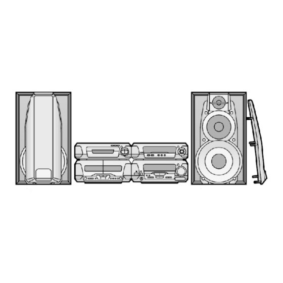
Page 2: Location Of Controls
1. Note Refer to the service manual for Model No. SA-EH590EG, SA-EH590EP (Order No. AD0302008C8) for information on Accessories and Packaging. 2. Location of Controls 3. Operation Checks and Component Replacement / Procedures - This section describes procedures for checking the operation of the major printed circuit boards and replacing the main components. - Page 4 - Check the operation P.C.B. as shown below. 3.3. Replacement for the motor ass’y, capstan belt and winding belt - Follow the (Step 1) - (Step 3) of item 3.1.
- Page 5 - Follow the (Step 1) - (Step 7) of item 3.2.
- Page 8 3.4. Replacement for the components parts on the mechanism P.C.B. - Follow the (Step 1) - (Step 3) of item 3.1. - Follow the (Step 1) - (Step 7) of item 3.2. - Follow the (Step 1) - (Step 4) of item 3.3.
- Page 9 3.5. Replacement for the pinch roller ass’y and head block - Follow the (Step 1) - (Step 3) of item 3.1. - Follow the (Step 1) - (Step 7) of item 3.2. - Follow the (Step 1) - (Step 5) of item 3.3. 3.6.
- Page 10 3.7. Replacement for the cassette holder - Follow the (Step 1) - (Step 3) of item 3.1. - Follow the (Step 1) - (Step 11) of item 3.2.
- Page 11 4. To Supply Power Source This unit is designed to operate on power supplied from system connected. / When a component requires service, use the system connections to supply power source. / For system connections, refer to Fig.4-1. Fig. 4-1. 5.
- Page 12 5.2. Selecting service mode 1. Turn on the power to the unit. 2. Make sure that no tape is inserted in the cassette deck. (Service mode cannot be selected with a tape inserted in the cassette deck.) 3. Press the DOLBY NR button for about 2 seconds, and keep pressing it, also press the STOP button for about 2 seconds.
- Page 13 pressed, the fault items are displayed in sequence. Fig. 5-2. Table 5-1. FL display Symptom Cause Cassette deck does not operate correctly. Faulty cassette deck mechanism mode switch (Deck 1: S951, Deck 2: S971), plunger and capstan motor. / (Check and replace) Unit does not record or the unit goes into Faulty erasure prevention tabs detect switch recording mode even when the erasure...
- Page 14 cassette holder. Refer to Fig. 5-3. 3. Insert a metal tape into the Deck 2 with an intact erasure prevention tab on the right side. 4. Close the Deck 2 cassette holder. 5. Press the Fast forward button. Refer to Fig.
- Page 15 5.5. Exiting service mode 1. Press the STOP button for more than 5 seconds. (Diagnostic contents stored in memory for both Deck 1 and 2 are erased.) 2. Remove the cassette tape from the cassette holder. 3. Turn off the unit. 6.
- Page 16 Fast forward, TPS switch ( S907: Forward side playback switch ( S909: Reverse side playback switch ( S910: Rewind, TPS switch ( S911: Reverse mode switch / (REV MODE) S912: Deck 1/deck 2 select switch / (DECK 1/2) S913: Counter display switch / (COUNTER DISPLAY) S914: Counter reset switch / (COUNTER RESET) S915:...
- Page 17 S974: Deck 2 reverse side record prevention tab detect switch S975: Deck 2 forward side record prevention tab detect switch S976: Deck 2 METAL tape detect switch VR101: Deck 1 playback gain adjustment VR / (R ch) VR102: Deck 2 playback gain adjustment VR / (L ch) VR103: Deck 2 playback gain adjustment VR / (R ch) VR104:...
- Page 18 When replacing any of components, be sure to use only manufacturer’s specified parts shown in the parts list. - The supply part number is described alone in the replacement parts list. - Caution! IC and LSI are sensitive to static electricity. Secondary trouble can be prevented by taking care during repair.
- Page 19 Terminal Function Name Power supply terminal VREF Reference voltage input GND terminal O Muting control signal output O Deck 1 solenoid control signal output O Deck 1 motor drive control signal output HALT Power failure detect signal input Serial communication request signal input Serial communication complete signal input...
-
Page 20: Frequency Counter
Terminal Function Name O Deck 2 solenoid control signal output O Deck 2 motor drive control signal output 31 ENC/DEC O Dolby NR record/playback mode select signal output 32 DOLBY O Dolby NR ON/OFF control signal ON/OFF output E CS EEPROM chip select signal output (Not used, open) - Page 21 - AF Oscillator - Test tape - Head azimuth adjustment (8 kHz, -20 dB): QZZCFM - Tape speed adjustment (3 kHz, -10 dB): QZZCWAT - Playback gain adjustment (315 Hz, 0 dB): QZZCFM - Recording/playback frequency response check: QZZCFM / (315 Hz, -20 dB, 12.5 kHz~63 Hz, -20 dB) QZZCRA4 (Normal blank tape) QZZCRX2 (CrO2 blank tape) QZZCRZ6 (Metal blank tape)
- Page 22 13.4. Tape speed adjustment / (Deck 1/2) Note: When connecting the unit to other system components for test, short the section between the test point TP604 and TP609 and turn on the entire system. (The unit is set to the TEST mode, and either Deck 1 or Deck 2 indicatorwill blink.) Normal speed (Standard value: 3000 ±...
- Page 23 [Standard value:265 mV ~ 300 Fig. 13-4. 13.6. Erase current confirmation (Deck 2) 1. Connect the measuring instrument as shown in Fig. 13-5. 2. Insert the blank tape into Deck 2, and press the Record pause button. 3. Check if the output at this time between the erase current confirmation point TP301 and TP302 (the output on both edged of R313) is within the standard value shown below.
- Page 24 output as a reference (0 dB). 3. Confirm the playback frequency response is within the range shown in Fig. 13-7. Fig. 13-6. Fig. 13-7. 13.8. Recording/playback / frequency response and gain check (Deck 2) 13.8.1. Normal tape check 1. Connect the measuring instrument as shown in Fig.
- Page 25 13.8.2. CrO2/Metal tape check 1. Connect the measuring instrument as shown in Fig. 13-8. 2. Insert a CrO2/Metal tape into Deck 2. 3. Record signals at 50 Hz, 100 Hz, 200 Hz, 500 Hz, 1 kHz, 2 kHz, 10 kHz and 12.5 kHz (28 mV). 4.
- Page 26 Fig. 13-11. 14. Checking Procedure for Self-operation of Cassette Mechanism Ass’y - This procedure describes simple methods independent of mechanism controller or governor circuit. 14.1. Operation Check Providing with Cassette Tape 1. Push up the EJECT lever with rubber band. (Refer to Fig.
- Page 27 Repeat the above operation to FWD PLAY mode. Note: Incorrect duration for power supply may be operated to other mode. 14.1.1. Connection Diagram Between the Mechanism Ass’y and Power Supply / (MOTOR and Plunger) Fig. 14-1. 14.1.2. Detail View of EJECT Lever / (EJECT lever fixed by rubber band, Plunger rib operation) Fig.
- Page 28 15. Replacement Parts List Notes: - Important safety notice: Components identified by mark have special characteristics important for safety. Furthermore, special parts which have purposes of fire-retardant (resistors), high-quality sound (capacitors), low-noise (resistors), etc. are used. When replacing any of components, be sure to use only manufacture’s specified parts shown in the parts list.
-
Page 29: Table Of Contents
SCREW RGR0287A-P REAR PANEL RKA0105-K RUBBER RKA0106-N FOOT RING RMN0539 CABLE HOLDER RDG0129-1 DAMPER GEAR REX0966-1 WIRE ASS'Y RGB0025-A TECHNICS BADGE RGK1131-2S ORNAMENT(L) RGK1132-2S ORNAMENT(R) RGL0441-Q PANEL LIGHT REZ1194 WIRE ASS'Y RKF0462-K2 CASSETTE HOLDER(L) RKF0463-K2 CASSETTE HOLDER(R) RKF0587G-2S CASSETTE LID(L) - Page 30 Ref. No. Part No. Part Name & Description Remarks RMR0909-X PCB HOLDER RED0037 HEAD BLOCK ASS'Y / (R/P) L1AA00000008 101-1 RHD17015 SCREW RED0038 HEAD BLOCK ASS'Y / (P.B) 102-1 RHD17015 SCREW RDG0300 REEL TABLE BASE RDG0301 GEAR RDK0026 GEAR RDV0033-4 BELT1 RDV0034-1 BELT2...
- Page 31 Ref. No. Part No. Part Name & Description Remarks C129 ECEA1AKS220 10V 22U C130 F2A1C101A133 16V 100U C131-34 ECJ2VB1H471K 50V 470P C135,36 ECA1HAK010XI 50V 1U C137 ECEA1HKS0R1 50V 0.1U C138 F1J1E4730004 25V 0.047U C139 ECEA0JKS470 6.3V 47U C140 ECEA1CKS100 16V 10U C141 ECA1HAK010XI 50V 1U...
- Page 32 Ref. No. Part No. Part Name & Description Remarks CS971 RJU071H09M CONNECTOR(9P) K1KB09C00001 D101,02 MA2J11100L DIODE D301 MA2J11100L DIODE D606 MAZ40560MF DIODE D651,52 MA165TA5 DIODE MA2C16500E D701 MA2J11100L DIODE D705,06 MA2J11100L DIODE D707 MA4051M DIODE MAZ40510M D708-10 MA2J11100L DIODE D904 MA2J11100L DIODE D905...
- Page 33 Ref. No. Part No. Part Name & Description Remarks Q902-04 DTC143EUT106 TRANSISTOR B1GBCFGG0006 R101,02 ERJ6GEYJ562V 1/10W 5.6K R103,04 ERJ6GEYJ104V 1/10W 100K R105,06 ERJ6GEYJ334V 1/10W 330K R107,08 ERJ6GEYJ103V 1/10W 10K R109,10 ERJ6GEYJ102V 1/10W 1K R111 ERJ6GEYJ820V 1/10W 82 D0GD820JA012 R112 ERJ8GEYJ820V 1/8W 82 R113 ERJ6GEYJ123V...
- Page 34 Ref. No. Part No. Part Name & Description Remarks R305 ERJ6GEYJ183V 1/10W 18K R306 ERJ6GEYJ333V 1/10W 33K R307 ERDS1FJ2R2 1/2W 2.2 R308 ERJ6GEYJ102V 1/10W 1K R309-11 ERJ6GEYJ472V 1/10W 4.7K R313 ERDS2TJ1R0 1/4W 1.0 R602 ERQ16NKWR33E 1/6W 0.33 R603 ERD2FCG100 1/4W 10 R604 ERJ6GEYJ331V 1/10W 330...
- Page 35 Ref. No. Part No. Part Name & Description Remarks R903 ERJ6GEYJ152V 1/10W 1.5K R904 ERJ6GEYJ182V 1/10W 1.8K R905 ERJ6GEYJ222V 1/10W 2.2K R906 ERJ6GEYJ332V 1/10W 3.3K D0GD332JA003 R908 ERJ6GEYJ122V 1/10W 1.2K D0GD122JA003 R909 ERJ6GEYJ152V 1/10W 1.5K R910 ERJ6GEYJ182V 1/10W 1.8K R911 ERJ6GEYJ222V 1/10W 2.2K R914...
- Page 36 17. Mechanism Parts Location...
- Page 38 18. Schematic Diagram for printing with letter size F0302KH...
- Page 39 OPERATION CIRCUIT :POSITIVE VOLTAGE LINE :PLAYBACK SIGNAL LINE Q901 S907 DTA143EUT106 D907 SML79455C LED DRIVE Q903 R916 DTC143EUT106 S912 S906 LED DRIVE(FWD) (DECK 1/2) 4.2V S911 S905 (REV MODE) (DOLBY NR) D905 SML79455C R914 Q904 S910 S904 ( REC PAUSE) DTC143EUT106 R915 LED DRIVE(REV)
- Page 40 MAIN CIRCUIT :POSITIVE VOLTAGE LINE : RECORDING SIGNAL LINE : PLAYBACK SIGNAL LINE R101 C123 5.6K 25V4.7 R157 9.6V C150 (0.2V) Q101 C143 C115 10V100 DECK1 CP101 470P 470P 2SJ164RTA HEAD SELECT (REC:ON) C117 330P PLAYBACK HEAD C129 R117 R725 10V22 2.2K IC101...
- Page 41 : PLAYBACK SIGNAL LINE DOLBY R725 2.2K C207 270P C203 R209 R211 R221 C225 25V4.7 L201 25V4.7 C205 50V1 C218 R237 R220 50V0.1 (9.6V) 0.1V DOLBY ON : 0V (0.1V) 4.8V 9.6V 4.7V 4.7V 4.6V 4.7V 0.4V 4.8V 9.6V ON/OFF IC201 CXA1552M-T4 DOLBY B NR...
- Page 42 MAIN CIRCUIT :POSITIVE VOLTAGE LINE : RECORDING SIGNAL LINE : PLAYBACK SIGNAL LINE Q807 Q809 Q810 Q808 2SB621ARSTA DTC143EUT106 DTC143EUT106 2SB621ARSTA SOLENOID DRIVE SOLENOID DRIVE SOLENOID DRIVE SOLENOID DRIVE 10.3V R802 R823 R824 R812 10.3V 10.3V 10.3V 10.2V 10.2V 10.3V Q803 Q805 2SD592ARSTA...
- Page 43 LAYBACK SIGNAL LINE 4.8V Q701,703 2SD1819ARTX R738 R747 5ms. 2V/DIV. INTERFACE 4.8V R704 16 ms. 1.9V 4.7K 0.1V 3.6V Q701 R708 16ms. 1.8V 4.7K 1.2V R737 R736 Q703 F=8MHz R705 L701 R711 10 H 100K R722 0.2V C706 0.6V 50V3.3 1 2 3 4 5 6 7 8 9 10 11 12 13 14 15 16 17 18 19 20 21 CN901 X701...
- Page 44 OPERATION CIRCUIT :POSITIVE VOLTAGE LINE :PLAYBACK SIGNAL LINE Q901 S907 D907 DTA143EUT106 SML79455C LED DRIVE Q903 R916 DTC143EUT106 S912 S906 LED DRIVE(FWD) ( DECK 1/2 ) 4.2V S911 S905 ( REV MODE ) ( DOLBY NR ) D905 SML79455C R914 Q904 S910 S904...
- Page 46 BA7755AF CXA1998BQT6 0N2180RLC1 2SD1450RSTA CXA1552M-T4 16PIN MC14066BFEL 14PIN M38503M2406F 42PIN No.1 2SB621ARSTA 2SD1819ARTX 2SC3940AQSTA 2SD2144STA 2SJ164QTA 2SJ164RTA 2SD592ARSTA 2SD1328STXRA DTA143EUT106 DTC114EUT106 DTC143EUT106 DTC144EUT106 MA165TA MA4051MTA SML79455C MA111TX MA4056MTA Cathode Cathode Anode Cathode Anode Cathode Anode Anode Anode...
- Page 47 [DECK 2] [DECK 1] EARTH TERMINAL P.C.B. R/P HEAD, PLAYBACK ERASE HEAD HEAD W601 1 . . . 5 1 . . . 5 1 . 5 1 . 5 W601 CP101 CP102 MAIN P.C.B. To DVD CHANGER, CD CHANGER, CD PLAYER &...
- Page 49 MC14066BFEL NOTES : PLAYBACK SIGNAL LINE IC202 : RECORDING SIGNAL LINE SIGNAL CONT. ) indicates pin No. Right channel. To DVD CHANGER, CD CHANGER, CD PLAYER CXA1552M-T4 BLOCK DIAGRAM & IC201 SOUND PROCESSOR DOLBY B NR BLOCK DIAGRAM Q108 MC14066BFEL (11) CN601 SWITCH-...
- Page 50 Note: This printed circuit board diagram may be modified at any time with the development of new technology. EARTH TERMINAL P.C.B. OPERATION P.C.B. MAIN P.C.B. W601 Q303 Q306 L301 E C B S901 Q305 C302 OPEN) Q301 C303 E C B (REP2827E-M) Q304 S904...
- Page 51 MAIN CIRCUIT :POSITIVE VOLTAGE LINE : RECORDING SIGNAL LINE : PLAYBACK SIGNAL LINE R101 C123 5.6K 25V4.7 R157 9.6V C150 Q101 (0.2V) C143 C115 10V100 DECK1 CP101 470P 470P 2SJ164RTA HEAD SELECT (REC:ON) C117 330P DOLBY PLAYBACK HEAD C129 R117 R725 10V22 2.2K...
- Page 52 MAIN CIRCUIT :POSITIVE VOLTAGE LINE : RECORDING SIGNAL LINE : PLAYBACK SIGNAL LINE 4.8V Q701,703 Q807 Q809 Q810 Q808 2SD1819ARTX R738 R747 2SB621ARSTA DTC143EUT106 DTC143EUT106 2SB621ARSTA 5ms. 2V/ DIV. INTERFACE SOLENOID DRIVE SOLENOID DRIVE SOLENOID DRIVE SOLENOID DRIVE 10.3V 4.8V R802 R823 R824...
- Page 53 ORDER NO. AD0305100C8 Tuner/ Amplifier SA-DV290EE / SA-DV290GN Colour (S).......Silver Type System: SC-DV290 Because of unique interconnecting cables, when a compact requires service, send or bring in the entire system. SPECIFICATIONS Specification...
- Page 54 Amplifier section Power output (L/R both channel driven) Stereo Mode 2×25 W 1 kHz THD 1%/6 (High) 2×45 W 100 Hz THD 1%/8 (Low) RMS 1 kHz THD 10%/6 2×35 W (High) 2×65 W 100 Hz THD 10%/8 (Low) PRO LOGIC mode FRONT 2×25 W 1 kHz THD 1%/6...
- Page 55 Function Play timer (1 time, daily), Rec timer (1 time, daily) Sleep (120 min, 30 min intervals) Setting intervals (Play/Rec) 1 minute—23 hours 59 minutes (1 min intervals) General Power supply (For (GN) area) AC 230—240V 50Hz (For (EE) area) AC 230V 50Hz Power consumption 230 W...
- Page 56 (RJA0035-2X)....1 pc. - Remote control for (EE) area (EUR7702290)....1 pc. - Remote control for (GN) area (EUR7702300)....1 pc. - Remote control batteries (R6/LR6,”AA”,UM-3)....1 pc. Note: These are available on sales route.
- Page 57 - FM indoor antenna for (EE) area (N1EAYY000002)....1 pc. - FM indoor antenna for (GN) area (N1EAYY000001)....1 pc. - AM loop antenna set (N1DAEYA00008)....1 pc. - Speaker leads (REE1234-1)....2 pc. (Red/Black) (REE1233-1)....2 pc. (Gray/Blue)
- Page 58 - Video cord (K2JA2A000018)....1 pc. - RCAJ adaptor for (EE) area (K1JZ24D00002)....1 pc. 2. Before Repair and Adjustment 1. Turn off the power supply. Using a 10 , 10W resistor, connect both ends of power supply capacitors (C701-704) in order to discharge the voltage.
- Page 59 *No sound is heard when the power is supplied. *Sound stops during a performance. The functions of this circuitry is to prevent circuitry damage, for example, the positive and negative speaker connection wires are “shorted”, or if speaker systems with an impedande less than the indicated rated impedance of thisunitareused.
- Page 60 5.2. Checking for the operation P.C.B. - Follow the (Step 1) - (Step 3) of item 5.1. - Check the operation P.C.B. as shown below. 5.3. Checking for the main P.C.B.
- Page 61 - Follow the (Step 1) - (Step 3) of item 5.1.
- Page 62 - Check the main P.C.B. as shown below. 5.4. Replacement for the regulator transistor...
- Page 63 - Follow the (Step 1) - (Step 3) of item 5.1. 5.5. Replacement for the power IC - Follow the (Step 1) - (Step 3) of item 5.1. - Follow the (Step 1) - (Step 6) of item 5.2. - Follow the (Step 1) - (Step 10) of item 5.3.
- Page 64 6. Self-Diagnostic Function This unit equipped with a self-diagnostic function which, in the event of a malfunction, automatically displays a code indicating the nature of the malfunction. Use this self-diagnostic function when servicing the unit. 6.1. To display the malfunction code U70 DVD: Automatically displays on the U70 DECK: tuner/amplifier when a...
- Page 65 6.2. To return to the normal display 1. For U70 DVD/U70 DECK - Press an any operation button on the tuner/amplifier. - To re-display the code, switch the power off (POWER STANDBY button), and then switch power back on again. 2.
- Page 66 - If U70 is displayed on the tuner/amplifier, the Cassette deck or DVD Changer cannot be operated by remote control. - Correction Procedure 1. To check for correct insertion of the flat cables. - Insert each connectors until you hear a click. - Insert the flat cables at the back of the unit in the order indicated.
- Page 67 - Correction procedure Faulty Tuner/Amplifier (SA-DV290) output IC (IC601). (When a DC voltage is applied to speaker terminals.) 7. To Supply Power Source This unit SA-DV290 is designed to operate on power supplied form system connected. For system connection, refer to Fig. 7-1. Fig.
- Page 68 Notes: Use only this method when checking the voltage etc.. In case of checking operations, use the system connections to supply power source. 8. Schematic Diagram Notes 8.1. Type Illustration of IC's, Transistors and Diodes 8.2. Schematic Diagram Notes - This schematic diagram may be modified at any time with the development of new technology.
- Page 69 - S913: Digital super woofer (DIGITAL S. WOOFER) switch. - S914, 915: RDS display mode (RDS, PS-DISP, MODE-PTY) switches. For [EE] area. S914, 915: KARAOKE, Voice mute (KARAOKE, V.MUTE) switch. For [GN] area. - S916: Key control (KEY CON) switch. For [GN] area. - S917: MIC effect (MIC EFFECT, LOUNGE) switch.
- Page 70 9. Schematic Diagram 10. Printed Circuit Board Diagram 11. Block Diagram 12. Wiring Connection Diagram 13. Terminal Function of ICs 13.1. IC901 (C2BBFD000404): System Control/FL Drive Function Terminal Name CHECK Clock check signal input LC72 DO PLL data signal output for tuner unit (Z101) LC72 CE Chip enable signal output...
- Page 71 Function Terminal Name SH REQ Request signal output to Sound Processor 22 NC(GND) — Not used, connected to GND Volume control signal input JOGB JOGA MIC DET Microphone connecting detect signal input (Not used, connected to V HP SW Headphone connecting detect signal input RDS clock signal input RDS data signal input...
- Page 72 Function Terminal Name 85 CHORUS — LED (CHORUS) drive signal output (Not used, connected to V MUTE Muting signal output — Not used, oppen POWER Power control signal output — GND terminal Power supply terminal MUTE2 Muting signal output — Not used, open MUTE3 Muting signal output...
-
Page 73: Rex0966
(GN) RKW0581-1V FL WINDOW RMF0284 CUSHION (GN) RMN0427A CABLE HOLDER RYP1168-S FRONT PANEL ASS’Y (EE) RYP1168A-S FRONT PANEL ASS’Y (GN) 13-1 RGB0025-A TECHNICS BADGE 13-2 RGU1748-Q BUTTON,MIC EFFECT (GN) SHG1654 RUBBER XTB3+10JFZ SCREW XTB3+20JFZ SCREW XTB3+8JFZ SCREW XTW3+15T SCREW XTB3+12FFZ... - Page 74 Ref. No. Part No. Part Name & Description Remarks EUR7702290 REMOTE CONTROL (EE) EUR7702300 REMOTE CONTROL (GN) A1-1 UR64EC2337E BATTERY COVER K2JA2A000018 VIDEO CORD REE1233-1 SPEAKER LEADS(GRAY/BLUE) REE1234-1 SPEAKER LEADS(RED/BLACK) RJA0019-2X AC MAINS LEAD (EE) RJA0035-2X AC MAINS LEAD (GN) RQCA0801 QUICK SET-UP GUIDE RQT6895-R...
- Page 75 Ref. No. Part No. Part Name & Description Remarks C601,02 ECA1CAK100XB 16V 10U C603,04 ECBT1H471KB3 50V 470P C605,06 ECBT1H102KB3 50V 1000P C607,08 ECBT1H471KB3 50V 470P C609,10 ECBT1H560J3 50V 56P C611 F1D1H390A006 50V 39P C612 ECBT1H150JC3 50V 15P C613,14 ECBT1H470J3 50V 47P C616 ECEA1HKNR47B 50V 0.47U...
- Page 77 Ref. No. Part No. Part Name & Description Remarks C901 EEAFC0J101B 6.3V 100U C902 F2A1A102A018 10V 1000U C903,04 ECBT1H103KB5 50V 0.01U F1E1H1030001 C905 ECBT1H102KB3 50V 1000P C907,08 ECBT1H471KB3 50V 470P C909 ECBT1H102KB3 50V 1000P C910 ECBT1H200JC5 50V 20P F1D1H200A015 C911 F1D1H180A006 50V 18P C912...
- Page 78 Ref. No. Part No. Part Name & Description Remarks D730 MA4091H DIODE MAZ40910H D737 MA4082LTA DIODE MAZ40820LF D738-40 MA165TA5 DIODE MA2C16500E D741-44 B0AAMM000009 DIODE D745 MA4051M DIODE MAZ40510M D746 B0AAMM000009 DIODE D747 MA4068L DIODE MAZ40680L D751,52 1N5402BF DIODE D753-55 B0AAMM000009 DIODE D756,57 MA700...
- Page 80 Ref. No. Part No. Part Name & Description Remarks RPG4396 PACKING CASE(SA) RPG4397 PACKING CASE(RS) RPG4398 PACKING CASE(SH) RPG4399 PACKING CASE(SL) RPN1194 POLYFOAM(SA) RPN1195-2 POLYFOAM(RS) RPN1196 POLYFOAM(SH) RPN1197 POLYFOAM(SL) SPP740-1 PROTECTION COVER RPF0139-1 PROTECTION BAG(ACCESS.) RPG6349 PACKING CASE(SYSTEM) (EE) RPG6350 PACKING CASE(SYSTEM) (GN) RPQ0951...
- Page 81 Ref. No. Part No. Part Name & Description Remarks R404 ERDS2FJ471 1/4W 470 (GN) R405 ERDS2FJ472 1/4W 4.7K (GN) R406 ERDS2FJ474 1/4W 470K (GN) R407 ERDS2FJ472 1/4W 4.7K (GN) R409 ERDS2FJ472 1/4W 4.7K (GN) R410 ERDS2FJ222 1/4W 2.2K (GN) R411 ERDS2FJ331 1/4W 330 (GN)
- Page 82 Ref. No. Part No. Part Name & Description Remarks R649-52 ERDS1FJ100 1/2W 10 R683-86 ERDS2FJ102 1/4W 1K R687,88 ERDS2FJ152 1/4W 1.5K R691 ERDS1FJ680 1/2W 68 R692,93 ERDS2FJ102 1/4W 1K R694 ERDS2FJ223 1/4W 22K R695 ERDS2FJ471 1/4W 470 R696 ERDS2FJ473 1/4W 47K R708 ERDS2FJ472 1/4W 4.7K...
- Page 83 Ref. No. Part No. Part Name & Description Remarks R914 ERDS2FJ102 1/4W 1K R915 ERDS2FJ122 1/4W 1.2K R916 ERDS2FJ152 1/4W 1.5K R918 ERDS2FJ103 1/4W 10K R919 ERDS2FJ153 1/4W 15K R921,22 ERDS2FJ103 1/4W 10K R924,25 ERDS2FJ102 1/4W 1K R926 ERDS2FJ222 1/4W 2.2K R928 ERDS2FJ473 1/4W 47K...
- Page 84 Ref. No. Part No. Part Name & Description Remarks T701 ETP76VST617A POWER TRANSFORMER T702 ETP28KBZ21BG POWER TRANSFORMER VR401 EVUE27FK3B53 V.R.,MIC VOLUME (GN) VR901 EVQVBXFK124B V.R.,VOLUME X151 H0H433400001 OSCILLATOR (EE) X901 EF0EC6004T4 OSCILLATOR EFOEC6004T4 X902 H0A327200027 OSCILLATOR Z701 ENC471D5A J0LG00000008 Z901 B3RAD0000028 REMOTE SENSOR 15.
- Page 85 15.2. SA-DV290GN...
- Page 86 16. Packaging...
- Page 87 17. Schematic Diagram for printing with A4 size K0305 YH/HM...
- Page 88 : POSITIVE VOLTAGE LINE FAN MOTOR MAIN CIRCUIT : NEGATIVE VOLTAGE LINE :AUDIO SIGNAL LINE 7.6V 7.6V -10.4V Q556 JK551 2SC5398RSTA IC601 MOTOR DRIVE R566 RSN311W64B 4.7V FAN ON:0V 0.5V POWER AMP FAN ON:0V R568 C556 0.5V R570 16V10 2.2M Q557 C552 R559...
- Page 89 : POSITIVE VOLTAGE LINE : NEGATIVE VOLTAGE LINE MAIN CIRCUIT AC IN CIRCUIT : AUDIO SIGNAL LINE CN601 L605 SPEAKERS JK603 R649 JK601 C OUT CENTER(8 ) C OUT L604 HF(6 L602 R644 SPEAKERS R ch R640 SUR L IN L603 SUR L IN SURROUND(8 )
- Page 90 OPERATION CIRCUIT FL901 (A2BB00000115) FL DISPLAY 10 11 12 13 14 15 16 17 18 19 20 21 22 23 24 25 26 27 28 29 30 31 32 33 34 35 36 37 38 39 40 41 42 43 44 45 46 47 48 49 50 53 54 R996 A B C D...
- Page 91 : POSITIVE VOLTAGE LINE : NEGATIVE VOLTAGE LINE :AUDIO SIGNAL LINE :MIC SIGNAL LINE -30.1V A B C D E F G H I J K L M N O P Q R S T U V W X 5.1V Q901 For [GN] area.
- Page 92 : NEGATIVE VOLTAGE LINE :AUDIO SIGNAL LINE :MIC SIGNAL LINE OPERATION CIRCUIT : POSITIVE VOLTAGE LINE :TUNER SIGNAL LINE TUNER Lch/ TUNER Rc A.GN Lch I +B(10V 5.1V R941 VR901 EVQVBXFK124B (VOLUME) Z901 SOUND B3RAD0000028 Q902 PROCESSOR -B(-10V (REMOTE SENSOR) UN411FTA (SH-DV290) V.GN...
- Page 93 MAIN CIRCUIT 7.6V -10.4V W501 TUNER Lch/C TUNER Rch R511 R509 R597 C659 R631 A.GND 2.2K 16V10 3.9K Lch IN R512 47 R510 Rch IN C660 +B(10V) R598 R632 10.4V 16V10 3.9K 2.2K SUR L C202 SUR R SOUND PROCESSOR -B(-10V) -10.4V (SH-DV290)
- Page 94 : POSITIVE VOLTAGE LINE MAIN CIRCUIT : NEGATIVE VOLTAGE LINE :AUDIO SIGNAL LINE 7.6V -10.4V IC601 RSN311W64B POWER AMP -51.4V 54.1V -29.7V 29.4V -0.2V -29.3V 28.9V -59.5V 59.5V C648 1000P R612 C610 R620 120K R611 C609 R619 120K R610 150K R603 C612 R622...
- Page 95 FAN MOTOR 7.6V Q556 JK551 2SC5398RSTA MOTOR DRIVE R566 4.7V 0.5V FAN ON:0V FAN ON:0V R568 C556 0.5V R570 16V10 2.2M Q557 C552 R559 7.6V 2SA1995RSTA 0.01 4.7K -10.4V MOTOR DRIVE -10.4V -10.4V 0.3V R558 R591 Q555 2.2K 4.7K 2SD2144STA Q551 Q554 SIGNAL LEVEL DET.
- Page 96 : POSITIVE VOLTAGE LINE : NEGATIVE VOLTAGE LINE MAIN CIRCUIT : AUDIO SIGNAL LINE L605 SPEAKERS R649 JK601 HF(6 L602 R640 LF(8 L606 R650 JK602 HF(6 LF(8 L601 CP601 R639 C OUT C OUT SUR L OUT SUR L OUT SUR R OUT SUR R OUT CP602...
- Page 97 AC IN CIRCUIT CN601 JK603 C OUT CENTER(8 ) C OUT L604 R644 SPEAKERS R ch SUR L IN L603 SUR L IN SURROUND(8 ) SUR R IN R643 SUR R IN L ch R795 3.9K CN602 R712 2.2K SH SYNC SA SYNC D.GND Q726...
- Page 98 BU4053BCFE2 C2BBFD000404 RSN311W64B TA2011S 2SB1417PQTA 2SD2144STA C1BB00000527 2SD2137PQTA ....... 2SA1995RSTA 2SC3940AQSTA 2SB1548PQAU UN411FTA...
- Page 99 FAN MOTOR For [GN] area. To SOUND PROCESSOR SPEAKERS MIC1 MIC2 JK551 MIC JACK Z101 CP601 P.C.B. TUNER PACK W904B CP101 1 . . 4 MAIN P.C.B. CP602 ..W501 ..
- Page 101 W501 TUNER L/C FM ANT TUNER Rch A.GND BU4053BCFE2 IC201 Lch IN SIGNAL SELECTOR Rch IN Z101 TUNER PACK AM ANT RAN0005EM-2:EE +B(10V) ENG06502Q:GN SUR L SUR R SW CONT. To SOUND PROCESSOR BLOCK DIAGRAM -B(-10V) V.GND For [EE] area. D.GND CS/REQ C1BB00000527...
- Page 102 PHONES R ch RSN311W64B IC601 Q609 Q607 POWER AMP (18) (Q610) (Q608) MUTING MUTING Q606 MUTING D974 D601 POWER CONTROL CIRCUIT (25) Q605 SURROUND MUTING CENTER SPEAKERS Q902 Q612 (12) MUTING MUTING CONT. CONT. Q503,D558 SWITCH- POWER CONTROL/ PROTECTION CIRCUIT Q551,554, SIGNAL LEVEL DET.
- Page 103 Q702,705 REGULATOR T701 /STABILIZER D702,704, 752,754,755 D701,703, 751,753,761 Q703,704 REGULATOR Q723 NOTES : SIGNAL LINE L701 : AUDIO SIGNAL REGULATOR : TUNER SIGNAL Q701 AC IN : MIC SIGNAL Z701 REGULATOR RL702 ) indicates pin No. Right channel. AC IN D718,720 FP791 Q711,712,725...
- Page 104 Note: This printed circuit board diagram may be modified at any time with the development of new technology. MAIN P.C.B. OPERATION P.C.B. Q723 C740 D737 VR901 W902A (VOLUME) CP101 CN781 W902B Q609 R693 E C B [GN] area. R692 W501 E C B S913 R597...
- Page 105 POWER SUPPLY P.C.B. POWER TRANSFORMER (A) P.C.B. POWER TRANSFORMER R725 Q701 C717 (B) P.C.B. R723 T701(Power transformer) W701B Q705 CN701 E C B [GN] area. R794A Q702 CN711 CN702 R793 [EE] area. CN703 R749 W721B W722B Q711 CN713 CN704 Q725 CN705 R765 D730...
- Page 106 OPERATION CIRCUIT : POSITIVE VOLTAGE LINE : NEGATIVE VOLTAGE LINE :AUDIO SIGNAL LINE :MIC SIGNAL LINE -30.1V FL901 (A2BB00000115) A B C D E F G H I J K L M N O P Q R S T U V W X FL DISPLAY 10 11 12 13 14 15 16 17 18 19 20 21 22 23 24 25 26 27 28 29 30 31 32 33 34 35 36 37 38 39 40 41 42 43 44 45 46 47 48 49 50 53 54...
- Page 107 : NEGATIVE VOLTAGE LINE :AUDIO SIGNAL LINE :MIC SIGNAL LINE MAIN CIRCUIT OPERATION CIRCUIT : POSITIVE VOLTAGE LINE :TUNER SIGNAL LINE 7.6V -10.4V W501 TUNER Lch/C TUNER Rch R511 R509 R597 C659 R631 A.GND 2.2K 16V10 3.9K Lch IN R512 47 R510 Rch IN C660...
- Page 108 ORDER NO.AD0303068C8 Sound Processor SH-DV290EG Colour (S) ....Silver Type System: SC-DV290 Because of unique interconnecting cables,when a component requires servise,send or bring in the entire system. Note: Refer to the service manual for Model No. SA-DV290E/EG/EB (ORDER NO.AD0303067C2) for information on “ACCESSORIES”and “PACKAGING”. SPECIFICATIONS Specification...
- Page 109 EQ/SFP section MANUAL GEQ 5-Band EQ Center frequency 70/300/1 k/3.15 k/10 kHz Level control ±2.0, 4.0, 6.0 dB EQ/Space mode 4 modes HEAVY, CLEAR, SOFT, HALL SUPER 3D AI EQ 3 modes AI EQ, SUPER 3D AI 1, SUPER 3D AI 2 Pre-amplifier section Input sensitivity/impedance VCR (EXT)
- Page 110 1. Before Repair This equipment (SH-DV290), which is the component of the system, is supplied with power from the amplifier (SA-DV290).When repairing this equipment or checking operation of the system, be sure to connect the amplifier with it. Power supply and operation check in the state of it as a single equipmenet are impracticable. 2.
- Page 111 - Check the FL P.C.B. as shown below. 3.2. Checking for the main P.C.B. - Follow the (Step 1) - (Step 3) of item 3.1.
- Page 112 - Check the main P.C.B. as shown below.
- Page 113 4. Wiring Connection Diagram 5. Block Diagram 6. To Supply Power Source This unit is designed to operate on power supplied from system connected. When a component requires service, use the system connections to supply power source. For system connections. (Refer to Fig. 1) Fig.
- Page 114 - S601: Display mode (DISPLAY MODE) switch. - S602: DOLBY PRO LOGIC ( PRO LOGIC, OFF/ ON) switch. - S603: Super surround (SUPER SURROUND) switch . - S604: Super sound EQ (SUPER SOUND EQ) switch . - S605: Center focus (CENTER FOCUS) switch. - S606: Virtual rear surround (VIRTUAL REAR SURROUND) switch.
- Page 115 : Positive voltage line : CD Playback signal line : Negative voltage line 8. Schematic Diagram 9. Printed Circuit Board Diagram 10. Terminal Function of IC's 10.1. IC601(C2BBGF000425):System control/FL drive Mark I/O / Function Division KEY1 Operation key1 signal input terminal KEY2 Operation key2 signal input...
- Page 116 Mark I/O / Function Division DSP DO Data signal output terminal for IC401 DSP DI Data signal input terminal for IC401 JOGA JOG A signal input terminal JOGB JOG B signal input terminal CNVSS Connected to GND through resistor RESET System reset signal input terminal Not used, open...
- Page 117 Mark I/O / Function Division 37 LED SSS LED(SUPER SURROUND)signal output terminal 38 LED DPL LED(DOLBY PRO LOGIC) signal output terminal ORANGE LED (SEAT POSITION) signal output terminal 40 LED SPG GREEN LED (SEAT POSITION) signal output terminal 41 LED 3DO ORANGE LED (3D ENHANCED SURROUND) signal output terminal...
- Page 118 Mark I/O / Function Division CD REQ Serial data request signal output terminal for DVD DECK Serial data request signal output terminal for deck machanism CD& Chip select signal input DECK terminal (DVD and deck machanism) AVSS GND terminal VREF Reference voltage input terminal REG IN0...
-
Page 119: Rear Panel
Ref. No. Part No. Part Name & Description Remarks RKA0105-K RUBBER RKA0106-N FOOT RING RYP1176-S FRONT PANEL ASS’Y RGB0025-A TECHNICS BADGE RKW0576A-1V FL WINDOW RGK1242-S JOG RING ORNAMENT RGW0344-S1 JOG KNOB RGW0345-S JOY KNOB RMB0594 JOY SPRING RMQ0882 JOY LEVER... - Page 120 Ref. No. Part No. Part Name & Description Remarks C351,52 ECBT1C103MS5 16V 0.01U F1D1C103A004 C354 ECA1CAK100XB 16V 10U C356 ECA1CAK100XB 16V 10U C401 ECJ1VB1E223K 25V 0.022U C402,03 ECUVNH103KBV 50V 0.01U F1H1H103A748 C404 ECA0JAK470XH 6.3V 47U C501 ECBT1C103MS5 16V 0.01U F1D1C103A004 C502 ECBT1H331KB3 50V 330P...
- Page 121 Ref. No. Part No. Part Name & Description Remarks C811 ECJ1VB1E223K 25V 0.022U C812 ECJ1VB1C104K 16V 0.1U C813 ECUVNH103KBV 50V 0.01U F1H1H103A748 C814 ECJ1VB0J105K 6.3V 1U C815 ECJ1VB1E223K 25V 0.022U C816 ECJ1VB1C104K 16V 0.1U C818,19 ECJ1VB1H681K 50V 680P C820,21 ECEA1HKA4R7 50V 4.7U C822 ECA0JAK470XH...
- Page 122 Ref. No. Part No. Part Name & Description Remarks D605-10 MA165TA5 DIODE MA2C16500E D611,12 LNJ301MPUJAD D613-17 B3AHA0000012 D653 MA165TA5 DIODE MA2C16500E D761 MA4082LTA DIODE MAZ40820LF D762 B0AAMM000009 DIODE D763-66 MA165TA5 DIODE MA2C16500E D767 MA4051M DIODE MAZ40510M D770 MA4062H DIODE MAZ40620H D771 MA4051-L DIODE...
- Page 123 Ref. No. Part No. Part Name & Description Remarks Q506 UN411FTA TRANSISTOR UNR411F00A Q507 2SD2144S TRANSISTOR Q601 UN4211 TRANSISTOR UNR4211 Q602-04 2SC3311A TRANSISTOR 2SC3311AW Q605,06 UN5211TX TRANSISTOR UNR521100L Q761,62 2SD2137PQTA TRANSISTOR 2SD21370PA Q763 2SD592A TRANSISTOR 2SD0592AW Q764 2SB0621AHA TRANSISTOR Q765 2SC3311A TRANSISTOR 2SC3311AW...
- Page 124 Ref. No. Part No. Part Name & Description Remarks R315,16 ERDS2FJ274 1/4W 270K R317 ERDS2FJ223 1/4W 22K R318 ERDS2FJ101 1/4W 100 R319 ERDS2FJ154 1/4W 150K R322 ERJ3GEYJ822V 1/16W 8.2K D0GB822JA002 R323,24 ERDS2FJ120 1/4W 12 R325,26 ERDS2FJ102 1/4W 1K R327,28 ERDS2FJ561 1/4W 560 R329 ERDS2FJ564...
- Page 125 Ref. No. Part No. Part Name & Description Remarks R509 ERDS2FJ222 1/4W 2.2K R510 ERDS2FJ104 1/4W 100K R511 ERDS2TJ105 1/4W 1M R512 ERDS2FJ154 1/4W 150K R513 ERDS2FJ102 1/4W 1K R514 ERDS2FJ101 1/4W 100 R515 ERDS2FJ223 1/4W 22K R517 ERDS2FJ821 1/4W 820 R518 ERDS2FJ222 1/4W 2.2K...
- Page 126 Ref. No. Part No. Part Name & Description Remarks R691,92 ERDS2FJ221 1/4W 220 R716 ERDS2FJ821 1/4W 820 R761,62 ERDS2FJ2R2 1/4W 2.2 R763 ERQ16NKWR33E 1/6W 0.33 R764 ERDS2FJ821 1/4W 820 R765 ERDS2FJ221 1/4W 220 R766 ERDS2FJ182 1/4W 1.8K R767 ERDS2FJ102 1/4W 1K R768,69 ERDS2FJ122 1/4W 1.2K...
- Page 127 Ref. No. Part No. Part Name & Description Remarks R903 ERDS2TJ124 1/4W 120K S601-07 EVQ11G05R SW,PUSH S608-11 EVQ11G07K SW,JOY STICK S612,13 EVQ11G05R SW,PUSH S614 ESE24SV7 SW,MULTI JOG X401 RSXY8M00D01T OSCILLATOR H2B800400005 X601 H2B400400013 OSCILLATOR X801 RSXZ36M8M01T OSCILLATOR 12. Cabinet Parts Location...
- Page 128 13. Schematic Diagram for printing with A4 size K0304YH/HM...
- Page 129 Note: This printed circuit board diagram may be modified at any time with the development of new technology. OPERATION P.C.B. MAIN P.C.B. Q723 VR901 C740 (VOLUME) D737 W902A W902B CP101 CN781 Q609 R693 E C B S913 R692 DIGITAL W501 E C B S.WOOFER R597...
- Page 130 POWER TRANSFORMER (A) P.C.B. POWER TRANSFORMER (B) P.C.B. T701(Power transformer) AC IN P.C.B. CN701 R794 R795 Q791 D740 E C B RL702 CN711 CN702 T702(Power transformer) R793 D500 R773 CN703 W721B W722B R774 CN713 Q726 CN704 E C B C754 CN705 C758 CN712...
- Page 131 OPERATION CIRCUIT : POSITIVE VOLTAGE LINE : NEGATIVE VOLTAGE LINE :AUDIO SIGNAL LINE -30.1V FL901 (A2BB00000115) FL DISPLAY A B C D E F G H I J K L M N O P Q R S T U V W X 10 11 12 13 14 15 16 17 18 19 20 21 22 23 24 25 26 27 28 29 30 31 32 33 34 35 36 37 38 39 40 41 42 43 44 45 46 47 48 49 50 53 54 R996...
- Page 132 : NEGATIVE VOLTAGE LINE : AUDIO SIGNAL LINE MAIN CIRCUIT OPERATION CIRCUIT : POSITIVE VOLTAGE LINE : TUNER SIGNAL LINE 7.6V -10.4V W501 TUNER Lch/C TUNER Rch R511 R509 R597 C659 R631 A.GND 2.2K 16V10 3.9K Lch IN R512 47 R510 Rch IN C660 +B(10V)
- Page 133 : POSITIVE VOLTAGE LINE MAIN CIRCUIT FAN MOTOR : NEGATIVE VOLTAGE LINE :AUDIO SIGNAL LINE 7.6V 7.6V -10.4V Q556 IC601 2SC5398RSTA JK551 RSN311W64B SWITCHING R566 POWER AMP 4.7V 0.5V FAN ON:0V FAN ON:0V R568 C556 R570 0.5V 16V10 2.2M Q557 C552 R559 7.6V...
- Page 134 : POSITIVE VOLTAGE LINE MAIN CIRCUIT AC IN CIRCUIT : NEGATIVE VOLTAGE LINE :AUDIO SIGNAL LINE CN601 L605 SPEAKERS JK603 R649 JK601 C OUT CENTER(8 ) C OUT L604 HF(6 L602 R644 SPEAKERS R ch R640 SUR L IN L603 SUR L IN SURROUND(8 ) LF(8...
- Page 135 OPERATION CIRCUIT FL901 (A2BB00000115) FL DISPLAY 10 11 12 13 14 15 16 17 18 19 20 21 22 23 24 25 26 27 28 29 30 31 32 33 34 35 36 37 38 39 40 41 42 43 44 45 46 47 48 49 50 53 54 R996 A B C D...
- Page 136 : POSITIVE VOLTAGE LINE : NEGATIVE VOLTAGE LINE :AUDIO SIGNAL LINE -30.1V A B C D E F G H I J K L M N O P Q R S T U V W X 5.1V Q901 UN4212TA RESET -30.1V -25.6V FM / AM...
- Page 137 : NEGATIVE VOLTAGE LINE : AUDIO SIGNAL LINE OPERATION CIRCUIT : POSITIVE VOLTAGE LINE : TUNER SIGNAL LINE TUNER Lch/ TUNER Rc A.GN Lch I +B(10V R941 5.1V VR901 EVQVBXFK124B Z901 (VOLUME) SOUND B3RAD0000028 Q902 -B(-10V PROCESSOR (REMOTE SENSOR) UN411FTA (SH-DV290) V.GN MUTING CONT.
- Page 138 MAIN CIRCUIT 7.6V -10.4V W501 TUNER Lch/C TUNER Rch R511 R509 R597 C659 R631 A.GND 2.2K 16V10 3.9K Lch IN R512 47 R510 Rch IN C660 R632 +B(10V) R598 10.4V 16V10 3.9K 2.2K SUR L C202 SUR R SOUND -B(-10V) PROCESSOR -10.4V (SH-DV290)
- Page 139 : POSITIVE VOLTAGE LINE MAIN CIRCUIT : NEGATIVE VOLTAGE LINE :AUDIO SIGNAL LINE 7.6V -10.4V IC601 RSN311W64B POWER AMP -51.4V 54.1V -29.7V 29.4V -0.2V -29.3V 28.9V -59.5V 59.5V C648 1000P R612 R620 C610 120K R611 C609 R619 120K R610 150K C612 R622 120K...
- Page 140 FAN MOTOR 7.6V Q556 2SC5398RSTA JK551 SWITCHING R566 4.7V 0.5V FAN ON:0V FAN ON:0V R568 C556 0.5V R570 16V10 2.2M Q557 C552 R559 7.6V 2SA1995RSTA 0.01 4.7K -10.4V MOTOR DRIVE -10.4V -10.4V R558 0.3V R591 Q555 2.2K 4.7K 2SD2144STA Q551 Q554 SIGNAL LEVEL DET.
- Page 141 : POSITIVE VOLTAGE LINE MAIN CIRCUIT : NEGATIVE VOLTAGE LINE :AUDIO SIGNAL LINE L605 SPEAKERS R649 JK601 HF(6 L602 R640 LF(8 L606 R650 JK602 HF(6 LF(8 L601 CP601 R639 C OUT C OUT SUR L OUT SUR L OUT SUR R OUT SUR R OUT CP602 SH SYNC...
- Page 142 AC IN CIRCUIT CN601 JK603 C OUT CENTER(8 ) C OUT L604 R644 SPEAKERS R ch SUR L IN L603 SUR L IN SURROUND(8 ) SUR R IN R643 SUR R IN L ch R795 3.9K CN602 R712 2.2K SH SYNC SA SYNC D.GND Q726...
- Page 143 BU4053BCFE2 C2BBFD000404 RSN311W64B UN411FTA 2SB1417PQTA 2SD2144STA C1BB00000527 UN4211TA 2SD2137PQTA UN4212TA ....... 2SA1995RSTA 2SC3940AQSTA 2SB1548PQAU...
- Page 144 FAN MOTOR To SOUND PROCESSOR SPEAKERS JK551 Z101 CP601 TUNER PACK CP101 MAIN P.C.B. CP602 ..W501 ..W722A ..W901A .
- Page 147 Q607 (Q608) FM ANT W501 MUTING TUNER L/C TUNER Rch A.GND BU4053BCFE2 Lch IN IC201 Z101 TUNER PACK AM ANT SIGNAL SELECTOR (RAN0005EM-2) Rch IN Q605 +B(10V) MUTING SUR L SUR R SW CONT. To SOUND PROCESSOR BLOCK DIAGRAM Q902 -B(-10V) MUTING V.GND...
- Page 148 PHONES R ch RSN311W64B IC601 Q609 POWER AMP (18) (Q610) MUTING Q606 MUTING D974 D601 POWER CONTROL CIRCUIT (25) SURROUND C1BB00000527 IC151 RDS SIGNAL DEMODULATOR CENTER 3,11 SPEAKERS Q612 VDDA/D VREF FLOUT (12) MUTING CLOCK CONT. RECOVERY REFERENCE (57kHz) (1187.5kHz) VOLTAGE 4,10 VssA/D...
- Page 149 Q702,705 REGULATOR T701 /STABILIZER D702,704, 752,754,755 D701,703, 751,753,761 Q703,704 REGULATOR Q723 NOTES : SIGNAL LINE L701 : AUDIO SIGNAL REGULATOR : TUNER SIGNAL Q701 AC IN ) indicates pin No. Right channel. Z701 REGULATOR RL702 AC IN D717~720 FP791 Q711,712,725 Q791 REGULATOR RELAY...
- Page 150 ORDER NO.AD0305101C8 DVD/Video CD/CD changer SL-DV290EE / SL-DV290GN Colour (s)....Silver Type System:SC-DV290 Because of unique interconnecting cables, when a component requires service, send or bring in the entire system. Note: Refer to the service manual for Model No.SA- DV290EE/GN (ORDER NO.AD0305100C8) for information on “ACCESSORIES”...
- Page 151 Discs played (8 cm or 12 cm) DVD-Video/DVD-Audio DVD-RAM/R (DVD-Video format discs) Video CD, CD (CD-DA) MP3/WMA/JPEG format discs) Audio No. of channels 5.1 channel (FL, FR, SL, SR, C, SW) Video Signal system PAL 625/50, PAL 525/60, NTSC Output level Composite video 1 Vp-p (75 S-video Y...
- Page 152 processor with it. This equipment, even in the state of it as a single equipment, permits power supply and operation check. When operating it as a single equipment without the tuner/amplifierand sound processor, refer to the paragraph of "Measurements and Adjustments. 2.
- Page 153 a new unit. Connect the connector as short time as possible. 3. The flexible cable may be cut off if an excessive force is applied to it. Use caution when handling the cable. 4. The half-fixed resistor for laser power adjustment cannot be adjusted.
- Page 154 4.3. Grounding for electrostatic breakdown prevention 1. Human body grounding Use the anti-static wrist strap to discharge the static electricity from your body. (As shown in Fig. 3 .) 2. Work table grounding Put a conductive material (sheet) or steel sheet on the area where the optical pickup is placed, and ground the sheet.
- Page 155 5.1. Checking for the DVD module (1) P.C.B. - Check the DVD module (1) P.C.B. (A side) as shown below.
-
Page 156: Follow The (Step 1) - (Step 3) Of Item
- Check the DVD module (1) P.C.B. (B side) as shown below. 5.2. Checking for the operation P.C.B. - Follow the (Step 1) - (Step 3) of item 5.1. -
Page 158: Follow The (Step 1) - (Step 5) Of Item
- Check the operation P.C.B. as shown below. 5.3. Checking for the main P.C.B. - Follow the (Step 1) - (Step 3) of item 5.1. - Follow the (Step 1) - (Step 5) of item 5.2. - Check the main P.C.B. as shown below. - Page 159 5.4. Checking for the DVD module (2) P.C.B. - Follow the (Step 1) - (Step 3) of item 5.1. - Follow the (Step 1) - (Step 5) of item 5.2. - Check the DVD module (2) P.C.B. as shown below.
- Page 160 5.5. Replacement for the traverse unit - Follow the (Step 1) - (Step 3) of item 5.1. - Follow the (Step 1) - (Step 5) of item 5.2.
- Page 163 5.6. Replacement for the disc tray - Follow the (Step 1) - (Step 3) of item 5.1. - Follow the (Step 1) - (Step 5) of item 5.5.
- Page 166 5.7. Disassembly and reassembly for mechanism base drive unit - Follow the (Step 1) - (Step 3) of item 5.1. - Follow the (Step 1) - (Step 11) of item 5.5. - Follow the (Step 1) - (Step 9) of item 5.6.
-
Page 178: Follow The (Step 1) - (Step 7) Of Item
5.8. Replacement for the motor ass’y - Follow the (Step 1) - (Step 3) of item 5.1. - Follow the (Step 1) - (Step 5) of item 5.5. - Follow the (Step 1) - (Step 7) of item 5.6. - Page 179 5.9. Replacement for the optical pick-up - Follow the (Step 1) - (Step 3) of item 5.1. - Follow the (Step 1) - (Step 5) of item 5.2. - Follow the (Step 1) - (Step 11) of item 5.5.
- Page 182 6. Optical Pickup Self-Diagnosis and Replacement Procedure 6.1. Self-diagnosis The optical pickup self-diagnosis function and tilt adjustment check function have been included in this unit. When repairing, use the following procedure for effective Self-diagnosis and tilt...
- Page 183 adjustment.Be sure to use the self-diagnosis functionbeforereplacingthe optical pickup when "NO DISC" is displayed. As a guideline, you should replace the optical pickup when the value of the laser drive current is more than 55. Note: Press the power button to turn on the power, and check the value within three minutes before the unit warms up.
- Page 184 Cautions to be taken when replacing the optical pickup The optical pickup may break down due to the static electricity of human body. Take proper protection measures against static electricity before repairing the parts around the optical pickup. 1. Do not touch the areas around the laser diode and actuator. 2.
- Page 185 7. Self-Diagnosis Function and Service Modes Each results of self-diagnostic function and service mode is displayed on the LCD of Tuner / Amplifier (SA-DV290). When using these function, confirm the unit to be connected by system cable. 7.1. Self-diagnostic function for loading mechanism 7.1.1.
- Page 186 Table 7-1 Display code Cause Disc tray open detect switch (S3) fault. / (Check and replace) Clamp switch (S4) fault. / (Check and replace) Bottom switch (S5) fault. / (Check and replace) Tray position detect switch (S1, S2) fault. / (Check and replace) Disc load error.
- Page 187 Error Error Content Additional error explanation Defect 1 Defect 2 Defect 3 Code U, H error Focus error Tray loading error Spindle servo (Spindle servo, DSC SP motor, CLV error servo error) Traverse servo error Tracking servo error Seek error Power error Cannot switch off the power because of the panel and system computer...
- Page 188 Error Error Content Additional error explanation Defect 1 Defect 2 Defect 3 Code F603 Access failure to Access failure to CSS data of disc KEYDET caused by demodulation error F610 ODC abnormality No permission for command execution F611 6626 QCODE Access failure to seek address in CD don’t read Error series...
- Page 189 Error Error Content Additional error explanation Defect 1 Defect 2 Defect 3 Code F894 EEPROM EEPROM Serial / abnormality communication on lone F8A0 Message Begin sending message to AV task command is not appropriate 7.4. Last Error Code saved during NO PLAY Error Error Content System computer...
- Page 191 7.6. Sales demonstration lock function This function prevents discs from being lost when the unit is used for sales demonstrations by disabling the disc eject function. "LOCKED" is displayed on the unit, and ordinary operation is disabled. 7.6.1. Setting The sales demonstration lock is set by simultaneously pressing “STOP” button on the player and “PLAY”...
- Page 192 Do not disconnect the power plug from the outlet with the tray still open, then close the tray manually. 8. Service Precautions 8.1. Recovery after the DVD player is repaired - When a FROM or module P.C.B. is replaced, carry out the recovery processing to optimize the drive.
- Page 193 b. If No is selected, only recovery is performed. 5. a. When updating is finished, remove the disc according to the message appearing on the screen. b. Remove the disc according to the message appearing on the screen. 6. Turn off the power. Note: If the AC power supply is shut down during version-up due to a power failure, the version-up is improperly carried out.
-
Page 194: Adjustment Procedures
1. Operation/display Key operations are as follows. Laser operation time ..... In STOP mode, main unit [STOP]+ remote controller [ Spindle motor operation time ..In STOP mode, main unit [STOP]+ remote controller [ To reset the timer, perform the following while displaying the time with above key operation. - Page 195 9.2. Important points in adjustment 9.2.1. Important points in optical adjustment - Before starting optical adjustment, be sure to take anti-static measures. - Optical pickup tilt adjustment is needed after replacement of the following components. 1. Optical pickup unit 2. Spindle motor unit 3.
-
Page 196: Remote Control Unit
Measurement point Adjustment point Mode Disc Tangential adjustment T01 (inner periphery) play DVDR-S15 or DVDT screw Tilt adjustment screw T43 (outer periphery) play Measuring equipment Adjustment value None (Main unit display for servicing is used.) Adjust to the minimum jitter value. 9.4.1.1. - Page 197 Jitter value depends on the model: 1. If the jitter value changes like B, the optimum point is easy to find. 2. If the jitter value changes like A, set the optimum point near the middle. 9.4.1.3. Check after adjustment Play test disc or any other disc to make sure there is no picture degradation in the inner, middle and outer peripheries, and no audio skipping.
- Page 198 10. To Supply Power Source Cautions: - It is very dangerous to look at or touch the laser beam. (Laser radiation is invisible.) With the unit turned “on”, laser radiation is emitted from the pickup lens. - Avoid exposure to the lase beam, especially when performing adjustments.
- Page 199 1. Connect a DC power supply to JK1-5pin and JK1-6pin and . Then adjust the outputs to 10V for 5pin (refer to Fig. 5 and Fig. 6) Fig. 5 Fig. 6 Note: Use only this method when checking the voltage etc.. In case of checking operations, use the system connections to supply power source.
- Page 200 12.1. Type Illustration of IC's, Transistors and Diodes 12.2. Schematic Diagram Notes This schematic diagram may be modified at any time with the development of new technology. Notes: - S1 : Tray position 1 detect switch. - S2 : Tray position 2 detect switch. - S3 : Tray open detect switch.
- Page 201 ( ): CD play [1kHz, L+R, 0dB] Important safety notice: Components identified by mark have special characteristics important for safety. Furthermore, special parts which have purpose of fire-retardant (resistors), high-quality sound (capacitors), low-noise (resistors), etc. are used. When replacing any of components, be sure to use only manufacture's specified parts shownintheparts list.
- Page 202 INITIAL/LOGO ABBREVIATIONS A0~UP ADDRESS ACLK AUDIO CLOCK AD0~UP ADDRESS BUS ADATA AUDIO PES PACKET DATA ADDRESS LATCH ENABLE AMUTE AUDIO MUTE AREQ AUDIO PES PACKET REQUEST AUDIO RF SERVO AMP INVERTED INPUT SERVOAMPOUTPUT ASYNC AUDIOWORDDISTINCTION SYNC BIT CLOCK (PCM) BCKIN BIT CLOCK INPUT BLACK DROP OUT BLKCK...
- Page 203 INITIAL/LOGO ABBREVIATIONS DACCK D/A CONVERTER CLOCK DEEMP DEEMPHASIS BIT ON/OFF DEMPH DEEMPHASIS SWITCHING DIG0~UP FL DIGIT OUTPUT DATA INPUT DMSRCK DM SERIAL DATA READ CLOCK DMUTE DIGITAL MUTE CONTROL DROPOUT DOUT0~UP DATAOUTPUT DATASLICERF (BIAS) DRPOUT DROP OUT SIGNAL DREQ DATA REQUEST DRESP DATA RESPONSE DIGITAL SERVO CONTROLLER...
- Page 204 INITIAL/LOGO ABBREVIATIONS IECOUT IEC958 FORMAT DATA OUTPUT IPFRAG INTERPOLATION FLAG IREF I (CURRENT) REFERENCE ISEL INTERFACE MODE SELECT LDON LASER DIODE CONTROL LASER POWER CONTROL LRCK L CH/R CH DISTINCTION CLOCK MA0~UP MEMORY ADDRESS MEMORY CLOCK MCKI MEMORY CLOCK INPUT MCLK MEMORY SERIAL COMMAND CLOCK...
- Page 205 INITIAL/LOGO ABBREVIATIONS READ ENABLE RFENV RF ENVELOPE RF PHASE DIFFERENCE OUTPUT (CD-ROM) REGISTER SELECT RSEL RF POLARITY SELECT RESET RESERVE SBI0, 1 SERIAL DATA INPUT SBO0 SERIAL DATA OUTPUT SBT0, 1 SERIAL CLOCK SERIAL DATA CLOCK SCKR AUDIO SERIAL CLOCK RECEIVER SERIAL CLOCK SCLK...
- Page 206 SYSTEM CLOCK INITIAL/LOGO ABBREVIATIONS TRACKING ERROR TIBAL BALANCE CONTROL BALANCE OUTPUT 1 BALANCE INPUT BALANCE INPUT BALANCE OUTPUT 2 TPSN OP AMP INPUT TPSO OP AMP OUTPUT TPSP OP AMP INVERTED INPUT TRCRS TRACKCROSSSIGNAL TRON TRACKINGON TRSON TRAVERSESERVO ON INITIAL/LOGO ABBREVIATIONS VBLANK V BLANKING...
- Page 207 INITIAL/LOGO ABBREVIATIONS X' TAL XALE X ADDRESS LATCH ENABLE XAREQ X AUDIO DATA REQUEST XCDROM X CD ROM CHIP SELECT X CHIP SELECT XCSYNC X COMPOSITE SYNC X DATA STROBE XHSYNCO X HORIZONTAL SYNC OUTPUT XHINT XHINTERRUPTREQUEST X' TALOSCILLATORINPUT XINT X INTERRUPT X MEMORY WRITE ENABLE X' TAL OSCILLATOR OUTPUT...
- Page 208 Mark Function Division Connected to power supply VREF AVSS — Connected to GND MUTE Mute control output terminal 5 PWCONT O DVD module power supply control output terminal SYNC Power failure detect signal input terminal C/SW Center/sub woofer speaker select signal output terminal 8 B_REQ Serial communication request signal input terminal...
- Page 209 input terminal Mark Function Division PSTN Position sensor detect signal input terminal Disc tray position 2 detect signal input terminal Disc tray position 1 detect signal input terminal Disc tray open detect signal input terminal Motor drive control signal output terminal (forward direction) Motor drive control signal output terminal (reverse...
-
Page 210: Spring
FFC(15P) REZ1391-J FFC(17P) REZ1392-J FFC(26P) RMX0210 SPACER RYF0592-1S TRAY ORNAMENT RKA0105-K RUBBER RKA0106-N FOOT RING RYP1174-S1 FRONT PANEL ASS’Y RGB0025-A TECHNICS BADGE XTB3+5JFZ SCREW XTBS3+8JFZ1 SCREW XTW3+8T SCREW RHD30007-1S SCREW RKM0399-S1 TOP CABINET REZ1377-J FFC(50P) RHD30090 SCREW REZ1314 FLAT CABLE... - Page 211 Ref. No. Part No. Part Name & Description Remarks XTB3+10J SCREW RMR0624-W5 CLAMPER RMR1367-K FIXED PLATE RMB0561 ASSIST LEVER SPRING RMR1121-K MECHANISM COVER RMQ0742 SPINDLE BASE RXQ0561 DISC TRAY RME0261 FRONT LOCK SPRING RMX0140 DISC SPACER RHM0001 MAGNET RMQ0749 UPPER SPINDLE RMX0141 SPACER XTW3+10T...
- Page 213 Ref. No. Part No. Part Name & Description Remarks ECEA1CKS101 16V 100U ECBA1E103ZF5 25V 0.01U ECA1CM332 16V 3300U ECA1CM471 16V 470U EEUFC0J821B 6.3V 820U ECJ1VB1H102K 50V 1000P ECEA1CKS100 16V 10U ECJ1VB1H102K 50V 1000P F1H1H103A748 50V 0.01U ECEA1AKS101 10V 100U ECEA1AKS221 10V 220U ECA0JM222 6.3V 2200U...
- Page 214 Ref. No. Part No. Part Name & Description Remarks C809,10 ECEA1CKS220 16V 22U C811,12 ECJ1VB1H222K 50V 2200P C813-16 ECEA1CKS100 16V 10U C817 ECJ1VF1C104Z 16V 0.1U C818 F2A0J4700007 6.3V 47U C819 ECEA1AKS101 10V 100U C821,22 ECEA1CKS100 16V 10U C823,24 F1H1H471A736 50V 470P C825,26 F1H1H470A736 50V 47P...
- Page 215 Ref. No. Part No. Part Name & Description Remarks C2501 EEVFC0J221P 6.3V 220U C2502 ECEV1CA101WP 16V 100U C2503 ECEV1CA220WR 16V 22U C2504-08 ECJ1VF1C104Z 16V 0.1U C2509 EEVFC1C100R 16V 10U C2510-13 ECJ1VF1C104Z 16V 0.1U C3001,02 F2G0J331A015 6.3V 330U C3003-18 ECJ1ZF1C104Z 16V 0.1U C3019 F1H0J1050013 6.3V 1U...
- Page 216 Ref. No. Part No. Part Name & Description Remarks C6215 ECJ1VB1C104K 16V 0.1U C6221-23 ECJ1ZF1C104Z 16V 0.1U C6251-53 F3F1A1060002 10V 10U C6254,55 ECJ1ZF1C104Z 16V 0.1U C6256 ECJ1VB1C104K 16V 0.1U C6257 EEE0JA101SP 6.3V 100U C6301,02 ECJ1ZF1C104Z 16V 0.1U C6503 ECJ1VC1H120J 50V 12P C6505 ECJ1VC1H150J 50V 15P...
- Page 217 Ref. No. Part No. Part Name & Description Remarks FP3203 K1MN15B00037 CONNECTOR(15P) FP4202 K1MN26B00037 CONNECTOR(26P) FP5101 K1MN30B00098 CONNECTOR(30P) FP5102 K1MN50B00010 CONNECTOR(50P) FP5201 K1MN50B00010 CONNECTOR(50P) C0GAM0000005 C0DBAJG00002 C0CAADG00019 C0CAADE00007 IC401 C2BBFD000402 IC501 C9ZB00000431 IC601 C0ZBZ0000040 IC801 C0JBAS000138 IC802-04 C0ABBB000125 IC805 C0ABBB000210 IC891 C0JBAR000292 IC2001...
- Page 218 Ref. No. Part No. Part Name & Description Remarks L501,02 G0BYYYY00016 COIL L503 ELJFCR68KF COIL L2001,02 G1C100K00020 COIL L2021 G1C100K00020 COIL L3001 G1C100K00020 COIL L3091 G1C100K00020 COIL L4211 G1C220KA0038 COIL L5101 ELJEA100KF COIL L5201,02 G1C100K00020 COIL L6561,62 G1C220KA0038 COIL LB3001,02 J0JHC0000045 COIL LB3201-03...
- Page 219 Ref. No. Part No. Part Name & Description Remarks FMW1T98 TRANSISTOR 2SB14170JA TRANSISTOR FMW1T98 TRANSISTOR 2SB14170JA TRANSISTOR FMW1T98 TRANSISTOR 2SB14170JA TRANSISTOR 2SB1218A TRANSISTOR FMW1T98 TRANSISTOR 2SB0766A0L TRANSISTOR 2SD08740WL TRANSISTOR Q303 B1GBCFJJ0007 TRANSISTOR Q304 2SB0621AHA TRANSISTOR Q305 UNR521N00L TRANSISTOR Q307,08 B1GBCFJJ0007 TRANSISTOR Q401 UNR521400L...
- Page 220 Ref. No. Part No. Part Name & Description Remarks R305,06 ERJ3GEYJ103V 1/16W 10K D0GB103JA002 R307 ERJ3GEYJ102V 1/16W 1K R308 ERJ3GEYJ221V 1/16W 220 R312 ERJ3GEYJ103V 1/16W 10K D0GB103JA002 R314 ERJ3GEYJ103V 1/16W 10K D0GB103JA002 R401 ERJ3GEYJ681V 1/16W 680 D0GB681JA002 R402 ERJ3GEYJ104 1/16W 100K R403 ERJ3GEYJ472V 1/16W 4.7K...
- Page 221 Ref. No. Part No. Part Name & Description Remarks R612 ERJ3GEYJ181V 1/16W 180 R613 ERJ3GEYJ223V 1/16W 22K D0GB223JA002 R614 ERJ3GEYJ123V 1/16W 12K R615 ERJ3GEYJ682V 1/16W 6.8K D0GB682JA002 R616 ERJ3GEYJ472V 1/16W 4.7K R617 ERJ3GEYJ332V 1/16W 3.3K D0GB332JA002 R618 ERJ3GEYJ222V 1/16W 2.2K R619 ERJ3GEYJ182V 1/16W 1.8K...
- Page 222 Ref. No. Part No. Part Name & Description Remarks R865,66 ERJ3GEYJ104 1/16W 100K R867 ERJ3GEYJ473V 1/16W 47K D0GB473JA002 R891,92 ERJ3GEYJ104 1/16W 100K R893 ERJ3GEYJ103V 1/16W 10K D0GB103JA002 R899 ERJ3GEY0R00V 1/16W 0 R2021 ERJ3GEYJ473V 1/16W 47K D0GB473JA002 R2022,23 ERJ3GEYJ752V 1/16W 7.5K R2025,26 ERJ3GEYJ223V 1/16W 22K...
- Page 223 Ref. No. Part No. Part Name & Description Remarks R5201 ERJ3GEY0R00Z 1/16W 0 R5203 ERJ3GEY0R00Z 1/16W 0 R5204 ERJ3GEYJ102V 1/16W 1K R5221 ERJ3GEY0R00Z 1/16W 0 R5231,32 ERJ3GEYJ822V 1/16W 8.2K D0GB822JA002 R5241 ERJ3GEYJ221V 1/16W 220 R5242 ERJ3GEYJ823V 1/16W 82K D0GB823JA002 R5257 ERJ3GEY0R00Z 1/16W 0 R5262...
- Page 224 Ref. No. Part No. Part Name & Description Remarks SJ313 ERJ3GEY0R00V 1/16W 0 X401 H2B800400005 OSCILLATOR X6501 H0J368600005 OSCILLATOR Z501-03 J0JBC0000015 COIL 19. Cabinet parts Location...
- Page 225 20. Loading Mechanism Parts Location 21. Traverse Mechanism Parts Location...
- Page 226 22. Schematic Diagram for printing with A4 size K0305 YH/HM...
- Page 227 SCHEMATIC DIAGRAM-4 DVD MODULE(AVDEC) CIRCUIT :POSITIVE VOLTAGE LINE :AUDIO/VIDEO SIGNAL LINE :AUDIO SIGNAL LINE :VIDEO SIGNAL LINE DVD MODULE (VIDEO DAC) LB3001 CIRCUIT on J0JHC0000045 27 26 25 24 23 22 21 20 19 18 17 16 15 14 13 12 11 10 9 8 7 6 5 4 3 2 SCHEMATIC D+1.5V DIAGRAM-5/1-G...
- Page 228 SCHEMATIC DIAGRAM-5 DVD MODULE(VIDEO DAC) CIRCUIT :POSITIVE VOLTAGE LINE :VIDEO SIGNAL LINE FL6255 VLF1491S104T DVD MODULE (FEP) CIRCUIT on M+9V SCHEMATIC DIAGRAM-2/12-G M.GND FL6253 F1H0J1050018 DVD MODULE (CPU) CIRCUIT on D+5V SCHEMATIC DIAGRAM-7/1-A D.GND DVD MODULE IC6251 FP3202 (FEP) CIRCUIT on D+5V D.GND C0DBEZG00011...
- Page 229 SCHEMATIC DIAGRAM-6 DVD MODULE(AUDIO DAC) CIRCUIT :POSITIVE VOLTAGE LINE :AUDIO SIGNAL LINE :SURROUND SP. SIGNAL LINE :CENTER SP. SIGNAL LINE :SUB WOOFER SIGNAL LINE DVD MODULE (AVDEC) CIRCUIT on SCHEMATIC DIAGRAM-4/12-A DMIXOUT FL4201 F1H0J1050018 DVD MODULE SBI1 FP4202 LB4208 VLP0155-T SBO1 (CPU) CIRCUIT on SBT1...
- Page 230 SCHEMATIC DIAGRAM-7 DVD MODULE(CPU) CIRCUIT :POSITIVE VOLTAGE LINE DVD MODULE DVD MODULE (AUDIO DAC) CIRCUIT on LB6201 (VIDEO DAC) CIRCUIT on VLP0146-T SCHEMATIC DIAGRAM-6/1-G FS18 NRST SCHEMATIC 3.3V D+3.3V DVD MODULE DIAGRAM-5/1-C D.GND IC6211 (AVDEC) CIRCUIT on PST596JNR SCHEMATIC DIAGRAM-4/1-F FS18 NRST RESET...
- Page 231 SCHEMATIC DIAGRAM-8 MODULE CIRCUIT (FP4202) MODULE CIRCUIT (FP3202) LOADING MOTOR CIRCUIT MAIN CIRCUIT on SCHEMATIC DIAGRAM-6/12-D,E on SCHEMATIC DIAGRAM-5/12-F,G : POSITIVE VOLTAGE LINE Q304 : AUDIO SIGNAL LINE 2SB621ARSTA TA7291P :SURROUND SP. SIGNAL LINE PLUNGER DRIVE MOTOR DRIVE :CENTER SP. SIGNAL LINE :SUB WOOFER SIGNAL LINE 24 23 22 21 20 R307...
- Page 232 SCHEMATIC DIAGRAM-9 MAIN CIRCUIT MODULE CIRCUIT(FP3203) : POSITIVE VOLTAGE LINE : AUDIO SIGNAL LINE : VIDEO SIGNAL LINE :SURROUND SP. SIGNAL LINE :CENTER SP. SIGNAL LINE :SUB WOOFER SIGNAL LINE on SCHEMATIC DIAGRAM-5/12-C 7.5V 7.5V 4 5 6 7 8 9 10 11 12 13 14 CN501 IC802 Q801,802...
- Page 233 SCHEMATIC DIAGRAM-10 : AUDIO SIGNAL LINE :CENTER SP. SIGNAL LINE MAIN CIRCUIT : POSITIVE VOLTAGE LINE : VIDEO SIGNAL LINE :SUB WOOFER SIGNAL LINE :SURROUND SP. SIGNAL LINE R503 Z501 L501 VLP0146-T JK501 VIDEO OUT R506 L502 Z502 VLP0146-T JK501 Z503 S-VIDEO OUT R507...
- Page 234 SCHEMATIC DIAGRAM-1 NOTE: The number which noted at the connectors on the schematic diagram as "SCHEMATIC DIAGRAM-1" or "SCHEMATIC DIAGRAM-2" INTERFACE CIRCUIT indicates the schematic diagram serial number located on the left corner in the schematic d FP2501 To FG UNIT R2503 (3.3V) 2.9V...
- Page 235 diagram as :POSITIVE VOLTAGE LINE :AUDIO/VIDEO SIGNAL LINE e left corner in the schematic diagram. R2503 1.7V 1.7V 1.7V 1.7V 1.7V 1.7V C2501 0GBG0000033 OCUS/TRACKING COIL, PINDLE/ TRAVERSE OTOR DRIVE 1.7V 1.7V (3.3V) R2507 RA2501 FP5102 D.GND R5107 D.GND MUTE4 D+5V D+5V R5108...
- Page 236 SCHEMATIC DIAGRAM-2 DVD MODULE(FEP) CIRCUIT :POSITIVE VOLTAGE LINE :AUDIO/VIDEO SIGNAL LINE R5241 LB5240 FP5201 VLP0146-T R5242 LB5218 D.GND VLP0146-T D.GND MUTE4 LB5202 D+5V J0JHC0000045 D+5V TRAYIN M+9V M+9V LB5203 M+9V J0JHC0000045 QR5241 M.GND UN511MTX M.GND M.GND POWER SUPPLY LB5205 TRAYREF VLP0146-T 3.3V MUTE12...
- Page 237 TRAY/ TRV VD10 DVD MODULE TRV-SW+ (VIDEO DAC) CIRCUIT on MUTE4 TRAY DRV SCHEMATIC DIAGRAM-5/12-A TRAY REF DVD MODULE (VIDEO DAC) CIRCUIT on D+5V SCHEMATIC DIAGRAM-5/1-G D.GND M+9V SCHEMATIC DIAGRAM-5/1-H L5201 M.GND A+5V SCHEMATIC DIAGRAM-5/1-F A.GND DVD MODULE 3.3V D+3.3V (VIDEO DAC) CIRCUIT on D.GND SCHEMATIC DIAGRAM-5/1-D...
- Page 238 SCHEMATIC DIAGRAM-3 DVD MODULE(SODC) CIRCUIT :POSITIVE VOLTAGE LINE :AUDIO/VIDEO SIGNAL LINE L2021 3.3V DVD MODULE L2002 (VIDEO DAC) CIRCUIT on D+1.8V SCHEMATIC DIAGRAM-5/1-E C2014 C2016 D.GND DVD MODULE L2001 1.8V (VIDEO DAC) CIRCUIT on D+3.3V 3.3V SCHEMATIC DIAGRAM-5/1-D D.GND DVD MODULE 3.3V 1 NINT0 NTRYCL 132...
- Page 239 L LINE STENABLE STD0 3.3V STD1 R2047 STD2 DVD MODULE STD3 (AVDEC) CIRCUIT on STD4 SCHEMATIC DIAGRAM-4/1-A STD5 R2046 STD6 C2023 STD7 STVALID SD10 STCLK SD11 R2045 C2024 R2044 C2025 3.3V R2043 NTRYCL 132 3.3V NEJECT 131 MONI3 130 R2042 MONI2 129 MONI1 128 MONI0 127...
- Page 240 SCHEMATIC DIAGRAM-4 DVD MODULE(AVDEC) CIRCUIT :POSITIVE VOLTAGE LINE :AUDIO/VIDEO SIGNAL LINE :AUDIO SIGNAL LINE DVD MODULE (VIDEO DAC) LB3001 CIRCUIT on J0JHC0000045 SCHEMATIC D+1.5V DIAGRAM-5/1-G D.GND DVD MODULE (VIDEO DAC) LB3002 CIRCUIT on J0JHC0000045 D+3.3V SCHEMATIC D.GND DIAGRAM-5/1-D C3005 C3003 RA3002 2.3V DVD MODULE...
- Page 241 :AUDIO SIGNAL LINE :VIDEO SIGNAL LINE 27 26 25 24 23 22 21 20 19 18 17 16 15 14 13 12 11 10 9 8 7 6 5 4 3 2 IC3062 C3ABPG000121 MEMORY 28 29 30 31 32 33 34 35 36 37 38 39 40 41 42 43 44 45 46 47 48 49 50 51 52 53 54 RA3005 Vss 156 2.3V...
- Page 242 SCHEMATIC DIAGRAM-5 DVD MODULE(VIDEO DAC) CIRCUIT :POSITIVE VOLTAGE LINE :VIDEO SIGNAL LINE FL6255 VLF1491S104T DVD MODULE (FEP) CIRCUIT on M+9V SCHEMATIC DIAGRAM-2/12-G M.GND FL6253 F1H0J1050018 DVD MODULE (CPU) CIRCUIT on D+5V SCHEMATIC DIAGRAM-7/1-A D.GND DVD MODULE IC6251 (FEP) CIRCUIT on D+5V C0DBEZG00011 D.GND...
- Page 243 FL6255 VLF1491S104T FL6253 F1H0J1050018 FP3202 D.GND M+9V FL6251 M+9V F1H0J1050018 M.GND 2.5V M.GND D+5V D+5V D.GND MAIN CIRCUIT(CN2) D.GND on SCHEMATIC D+2.5V DIAGRAM-8/11,12-H D+2.5V FL6254 D.GND F1H0J1050018 D.GND A+5V A+5V A.GND A.GND LB3203 DVD MODULE LB3202 (CPU) CIRCUIT on STATUS LB3201 SCHEMATIC DIAGRAM-7/1-C DSPCLK...
- Page 244 SCHEMATIC DIAGRAM-6 DVD MODULE(AUDIO DAC) CIRCUIT :POSITIVE VOLTAGE LINE :AUDIO SIGNAL LINE :SURROUND SP. SIGNAL DVD MODULE (AVDEC) CIRCUIT on SCHEMATIC DIAGRAM-4/12-A DMIXOUT SBI1 DVD MODULE SBO1 (CPU) CIRCUIT on SBT1 SCHEMATIC DIAGRAM-7/12-G STBDAC2 DVD MODULE (CPU) CIRCUIT on 3.3V SCHEMATIC DIAGRAM-7/1-H 37 RSTB FS18...
- Page 245 :SURROUND SP. SIGNAL LINE :CENTER SP. SIGNAL LINE :SUB WOOFER SIGNAL LINE FL4201 F1H0J1050018 FP4202 LB4208 VLP0155-T A.GND VLP0155-T LB4207 A.GND LB4210 VLP0155-T A.GND VLP0155-T LB4209 A.GND VLP0155-T LB4212 A.GND VLP0155-T LB4211 A.GND MAIN CIRCUIT LB4215 MIX R (CN301) A.GND LB4214 on SCHEMATIC MIX L...
- Page 246 SCHEMATIC DIAGRAM-7 DVD MODULE(CPU) CIRCUIT :POSITIVE VOLTAGE LINE DVD MODULE (AUDIO DAC) CIRCUIT on SCHEMATIC DIAGRAM-6/1-G FS18 NRST 3.3V DVD MODULE IC6211 (AVDEC) CIRCUIT on PST596JNR SCHEMATIC DIAGRAM-4/1-F FS18 NRST RESET DVD MODULE (SODC) CIRCUIT on 3.3V SCHEMATIC DIAGRAM-3/1-D FS18 NRST Q6215 3.3V...
- Page 247 DVD MODULE LB6201 (VIDEO DAC) CIRCUIT on VLP0146-T SCHEMATIC 3.3V D+3.3V DIAGRAM-5/1-C D.GND PS6201 D+3.3V RESERVED KMODE SCSIEN 258SY TEST TERMINAL 1968SY SBI1 SBO1 R6216 SBT1 D.GND DVD MODULE (AUDIO DAC) SBI1 CIRCUIT on SBO1 SCHEMATIC SBT1 STBDAC2 DIAGRAM-6/1-H SCHEMATIC CPUADR17 AC3H DIAGRAM-6/12-C...
- Page 248 SCHEMATIC DIAGRAM-8 LOADING MOTOR CIRCUIT MAIN CIRCUIT : POSITIVE VOLTAGE LINE Q304 : AUDIO SIGNAL LINE 2SB621ARSTA TA7291P :SURROUND SP. SIGNAL LINE PLUNGER DRIVE MOTOR DRIVE :CENTER SP. SIGNAL LINE :SUB WOOFER SIGNAL LINE R307 R306 CLAMP SW 0.4V 7.8V 7.8V 7.8V 0.4V...
- Page 249 MODULE CIRCUIT ( FP4202 ) MODULE CIRCUIT ( FP3202 ) IRCUIT on SCHEMATIC DIAGRAM-6/12-D,E on SCHEMATIC DIAGRAM-5/12-F,G Q304 2SB621ARSTA PLUNGER DRIVE 24 23 22 21 20 R307 R306 CN301 Q305 UN521NTX PLUNGER DRIVE D302 D303 D304 O P N D302-304 RL1N4003N02 Q307 DTC114EUA106...
- Page 250 SCHEMATIC DIAGRAM-9 MODULE CIRCUIT(FP3203) MAIN CIRCUIT : POSITIVE VOLTAGE LINE : AUDIO SIGNAL LINE : VIDEO S on SCHEMATIC DIAGRAM-5/12-C 4 5 6 7 8 9 10 11 12 13 14 CN501 R314 R801 C801 16V1 R893 R802 C802 1.8K 16V10 7.5V IC891...
- Page 251 DIO SIGNAL LINE : VIDEO SIGNAL LINE :SURROUND SP. SIGNAL LINE :CENTER SP. SIGNAL LINE :SUB WOOFER SIGNAL LINE 7.5V 7.5V IC802 Q801,802 NJM4580EDTE1 R809 2SD1328TX Q303 BUFFER AMP(C/SW) MUTING IC801 DTC114EUA106 C0JBAS000138 R801 C801 R805 R807 C809 R815 C813 R821 SIGNAL SELECTOR 16V10...
- Page 252 SCHEMATIC DIAGRAM-10 : AUDIO SIGNAL LINE :CENTER SP. SIGNAL LINE MAIN CIRCUIT : POSITIVE VOLTAGE LINE : VIDEO SIGNAL LINE :SUB WOOFER SIGNAL LINE :SURROUND SP. SIGNAL LINE R503 Z501 L501 VLP0146-T JK501 VIDEO OU R506 L502 Z502 VLP0146-T JK50 Z503 R507 VLP0146-T...
- Page 253 ND SP. SIGNAL LINE L501 JK501 VIDEO OUT L502 JK501 S-VIDEO OUT SYNC CD REQ CT.GND +B (10V) D.GND SCLK DATA To SOUND PROCESSOR(SH-DV290) V.GND & CASSETTE DECK(RS-DV290) S.WOOFER CENTER CD Rch OUT CD A.GND CD Lch OUT SUR R SUR L A.GND 1000P...
- Page 254 C1DB00000582 16PIN C9ZB00000431 34PIN C0FBBK000036 48PIN MN103S26EGA 176PIN C2BBFD000402 42PIN BU4053BCFE2 16PIN MN102H60GFD 100PIN AN22030A-VT 64PIN NJM4580EDTE1 8PIN C3ABPG000121 54PIN MN6775511 208PIN NJU3713GTE1 18PIN No.1 No.1 C0JBAS000138 C3FBND000098 TA7291P PST596JNR PQ1CZ31H2ZP BA4558FHTT1 C0JBAA000001 C0DBEZG00011 C3EBGC000033 C0JBAS000116 C0DBFFG00004 C0DBCGE00002 NJM78M05FA C0GBG0000033 LM2940T5M 2SB1417PQTA 2SB1218TX...
- Page 255 OPERATION P.C.B. WB601 1 ..8 1 ..8 WA601 To SOUND PROCESSOR& CASSETTE DECK MAIN P.C.B. VIDEO OUT/ S-VIDEO OUT CN301 CN501 1 ... . 14 26 .
- Page 257 S2501 D2001 (REST DET.) AN22030A-VT IC5201 149,151,158,160, FRONT END PROCESSOR 164,166,168,172 HDD8~15 RFDIF OPTICAL PICK-UP UNIT PEAK 3,31,57, HPFIN MONI 78,125,143, RFTE 156,162,169 HPFOUT MONI Q2001 D+3.3V MONI2 CRnet. LPFOUT 88,99, 109,116 LPFIN VIN7 D+3.3V PHOTO A+5V RFENV HOLD DETECTOR VIN8 D+3.3V FBAL...
- Page 258 C0DBCGE00002 IC6253 C0GBG0000033 M+9V IC2501 D+5V REGULATOR FOCUS/TRACKING D+5V COIL,SPINDLE/TRAVERSE C0DBEZG00011 MOTOR DRIVE D+3.3V IC6251 D+2.5V REGULATOR VO4+ C0DBFFG00004 M2502 TRIN (TRAVERSE MOTOR) IC6252 VO4- LEVEL BIAS1 D+2.5V REGULATOR D+1.8V SHIFT OPIN+ VO3+ 22~26, M2501 29~35 (SPINDLE MOTOR) A0~11 VO3- VIN3 LEVEL SHIFT...
- Page 259 C0FBBK000036 IC4211 BU4053BCFE2 8CH AUDIO D/A CONVERTER IC891 SIGNAL SELECTOR VOUT1 81~88 STD0~7 (VOUT2) 13(1) 14(15) (13) OUTPUT AMP AND 5,15,26,39,52,58, LOW-PASS FILTER BCKIN 66,75,89,103,131, SRCK 12(2) 144,152,157,165, LRCIN 175,184,194,203 LRCK SERIAL DIN1 INPUT ADOUT0 VOUT3 (VOUT4) (11) DIN2 OUTPUT AMP AND ADOUT1 LOW-PASS FILTER DIN3...
- Page 260 REGULATOR SYNC C0JBAS000138 Q8,9 CD REQ BA4558FHTT1 IC801 POWER SIGNAL SELECTOR IC805 D+2.5V CT.GND SUPPLY/ CT.GND PQ1CZ31H2ZP CONT. Q6,7 VREF L2,4 DC+10V POWER DC-DC A+5V SUPPLY/ +B(10V) CONVERTER D.GND CONT. LM2940T5M A.GND NJM4580EDTE1 D.GND IC802 (1/2) SCLK D+5V REGULATOR BUFFER DATA Q802 Q14,15...
- Page 261 Note: This printed circuit board diagram may be modified at any time with the development of new technology. LOADING MOTOR P.C.B. INTERFACE P.C.B. (SIDE : A) INTERFACE P.C.B. (SIDE : B) C5152 1 ......30 FP5101 (LOADING MOTOR) D5151...
- Page 262 DVD MODULE P.C.B. (SIDE : A) RA6203 RA6204 PS6201 K6301 K6303 R2047 L2001 R2046 R6207 R2045 R6208 R2044 C2001 L2002 R6210 R2043 IC6223 R2042 IC2101 IC6201 IC6221 C2002 R2052 RA6201 IC6222 C2021 R2023 RA6202 R2038 R2022 R2027 RA2022 K3002 C6201 R2028 R2025 RA6206...
- Page 263 DVD MODULE P.C.B. (SIDE : B) RA2021 R2036 IC6301 IC2001 Q2001 C3065 C3063 D2001 IC3061 QR5221 L5202 RA3013 RA3011 L6561 IC6561 Q5271 K3011 L6562 RA3053 IC3062 R3052 R3051 C6252 RA3051 K3007 C4211 LB4214 IC4211 C4219 SL-DV290(EE,GN) DVD MODULE(SIDE: B) P.C.B.
- Page 264 MAIN P.C.B. (SIDE : A) C802 CN501 CN301 L502 JK501 20 18 IC802 C807 Q307 Q308 Q891 C809 C801 VIDEO OUT/ L501 Q303 S-VIDEO OUT C830 C822 Q305 Q807 Q304 Q501 IC801 E C B Q802 IC803 C829 C827 C814 IC501 IC891 C813...
- Page 265 OPERATION P.C.B. (SIDE : A) DIRECT OPEN S609 C601 S610 S608 S607 S606 C602 (DISC4) IC601 WB601 (DISC3) (DISC1) (DISC5) (DISC2) S611 C604 OPEN/ C603 CLOSE) D602 D607 S605 (DOUBLE D601 S612 (DISC1) RE-MASTER) (CINEMA) S614 (DISC1) (A-B (CD EDIT) S613 REPEAT) S616...
- Page 266 SCHEMATIC DIAGRAM-1 NOTE: The number which noted at the connectors on the schematic diagram as "SCHEMATIC DIAGRAM-1" or "SCHEMATIC DIAGRAM-2" INTERFACE CIRCUIT :POSITIVE VOLTAGE LINE :AUDIO/VIDEO SIGNAL LINE indicates the schematic diagram serial number located on the left corner in the schematic diagram. FP2501 To FG UNIT R2503...
- Page 267 SCHEMATIC DIAGRAM-2 DVD MODULE(FEP) CIRCUIT :POSITIVE VOLTAGE LINE :AUDIO/VIDEO SIGNAL LINE TRAY/ TRV VD10 DVD MODULE R5241 TRV-SW+ LB5240 FP5201 (VIDEO DAC) CIRCUIT on VLP0146-T R5242 MUTE4 TRAY DRV SCHEMATIC DIAGRAM-5/12-A TRAY REF LB5218 D.GND VLP0146-T D.GND DVD MODULE MUTE4 LB5202 D+5V (VIDEO DAC) CIRCUIT on...
- Page 268 SCHEMATIC DIAGRAM-3 DVD MODULE(SODC) CIRCUIT :POSITIVE VOLTAGE LINE :AUDIO/VIDEO SIGNAL LINE L2021 STENABLE STD0 3.3V DVD MODULE STD1 L2002 R2047 STD2 (VIDEO DAC) CIRCUIT on DVD MODULE STD3 D+1.8V SCHEMATIC DIAGRAM-5/1-E (AVDEC) CIRCUIT on C2014 C2016 STD4 D.GND SCHEMATIC DIAGRAM-4/1-A STD5 R2046 STD6...
Need help?
Do you have a question about the RS-DV290EG and is the answer not in the manual?
Questions and answers