Table of Contents
Advertisement
SERVICE MANUAL
Dolby noise reduction manufactured under license
from Dolby Laboratories Licensing Corporation.
"DOLBY" and the double-D symbol a are trade-
marks of Dolby Laboratories Licensing Corporation.
Amplifier section
The following measured at AC 120/240 V, 50 Hz
DIN power output (Rated)
Continuous RMS power output (Reference)
Peak music power output (Reference)
Inputs
PHONO IN (phono jacks):
MIX MIC (phone jack):
VIDEO/MD (AUDIO) IN (phono jacks):
Outputs
PHONES (stereo phone jack):
VIDEO/MD (AUDIO) OUT (phono jacks):
SPEAKER:
MICROFILM
SPECIFICATIONS
140 + 140 watts
(8 ohms at 1 kHz, DIN)
170 + 170 watts
(8 ohms at 1 kHz, 10% THD)
3,000 watts
sensitivity 3 mV, impedance
47 kilohms
sensitivity 1 mV, impedance
10 kilohms
sensitivity 250 mV, impedance
47 kilohms
accepts headphones of 8 ohms or more
voltage 250 mV, impedance 1 kilohms
accepts impedance of 8 to 16 ohms.
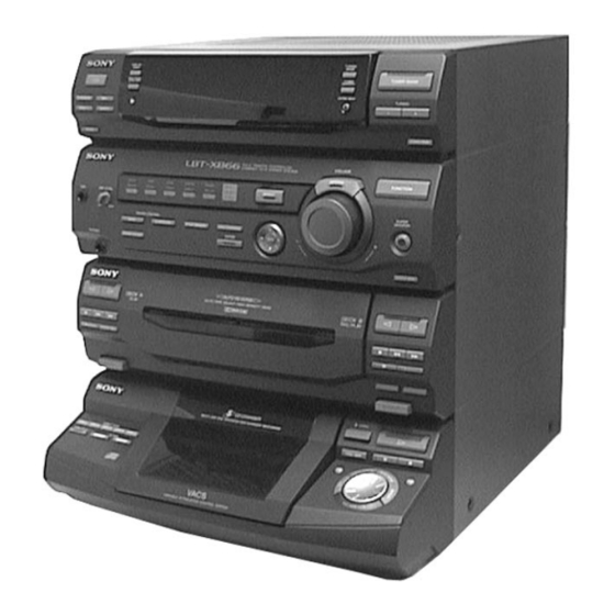
HCD-XB66K
Photo: XB66K
Model Name Using Similar Mechanism
CD
CD Mechanism Type
Section
Base Unit Name
Optical Pick-up Name
Tape deck
Model Name Using Similar Mechanism
Section
Tape Transport Mechanism Type
CD player section
System
Laser
Laser output
Wavelength
Frequency response
Signal-to-noise ratio
Dynamic range
CD DIGITAL OUT
(square optical connector jack, rear panel)
Wave length:
Output level:
COMPACT DISC DECK RECEIVER
E Model
HCD290/G330/XB3
CDM37LH-5BD29AL
BU-5BD29AL
KSS-213D/Q-NP
HCD-H881
TCM-220WR2
Compact disc and digital audio system
Semiconductor laser (λ = 780 nm)
Emission
duration: continuous
Max. 44.6 µW*
*This output is the value measured at
a distance of 200 mm from the
objective lens surface on the Optical
Pick-up Block with 7 mm aperture.
780 - 790 nm
2 Hz - 20 kHz (±0.5 dB)
More than 90 dB
More than 90 dB
600 nm
–18 dBm
– Continued on next page –
Advertisement
Chapters
Table of Contents

Related Manuals for Sony HCD-XB66K


Summary of Contents for Sony HCD-XB66K
- Page 1 HCD-XB66K SERVICE MANUAL E Model Photo: XB66K Dolby noise reduction manufactured under license Model Name Using Similar Mechanism HCD290/G330/XB3 from Dolby Laboratories Licensing Corporation. CD Mechanism Type CDM37LH-5BD29AL “DOLBY” and the double-D symbol a are trade- Section marks of Dolby Laboratories Licensing Corporation.
-
Page 2: Table Of Contents
4-track 2-channel stereo Frequency response (DOLBY NR OFF) SERVICING NOTES ..........3 60 - 13,000 Hz (±3 dB), using a Sony TYPE I cassette GENERAL ..............4 60 - 14,000 Hz (±3 dB), using a Sony TYPE II cassette DISASSEMBLY ............ -
Page 3: Servicing Notes
4-996-413-6π AND IN THE PARTS LIST ARE CRITICAL TO SAFE OPERATION. REPLACE THESE COMPONENTS WITH Saudi Arabia model 4-996-413-7π SONY PARTS WHOSE PART NUMBERS APPEAR AS Thai model 4-996-413-9π SHOWN IN THIS MANUAL OR IN SUPPLEMENTS PUB- LISHED BY SONY. -
Page 4: General
SECTION 2 This section is extracted from instruction manual. GENERAL LOCATION OF CONTROLS – Front Panel – 1 I /u (Power) button 2 DISPLAY/DEMO button 3 FILE (1-5) indicator 4 Fluorescent indicator tube !§ 5 TUNER MEMORY button 6 TUNING MODE button 7 TUNER/BAND button and indicator !¶... - Page 5 %º WAVE button %º %¡ %™ %£ %¢ %∞ %¡ SURROUND button %™ P FILE MEMORY button %£ GEQ CONTROL button %¢ P button and indicator (DECK B) %∞ p button (DECK B) %§ %§ ª button and indicator (DECK B) ^™...
- Page 6 – 6 –...
-
Page 7: Disassembly
SECTION 3 DISASSEMBLY • This set can be disassembled in the order shown below. FRONT PANEL OPTICAL MAIN CD MECHANISM CASE BASE UNIT BD BOARD SECTION SECTION DECK SECTION PICK-UP (Page 12) (Page 13) (Page 7) (Page 8) (Page 13) (Page 9) (Page 9) SLED... - Page 8 3-2. FRONT PANEL SECTION 1 Wire (flat type) (21 core) (CN205) 2 Wire (flat type) (11 core) (CN206) 3 Wire (flat type) (17 core) (CN102) 5 Front panel section 4 Four screws (BVTP3 × 8) 3-3. MAIN/KEY-CON BOARD 7 Back panel 5 Eleven screws (BVTP3 ×...
- Page 9 3-4. MAIN SECTION 1 Flat wire (CN202) 2 Connector (CN203) 4 Main section 3 Two screws (BVTP3 × 8) 3 Screw (BVTP3 × 8) 3 Two screws (BVTP3 × 8) 3-5. CD MECHANISM DECK SECTION (CDM37LH-5BD29AL) 3 Five screws (BVTP3 × 8) 4 CD mechanism deck section (CDM37LH-5BD29AL)
- Page 10 3-6. TAPE MECHANISM DECK SECTION (TCM-220WR2) 5 Three screws 5 Three screws (BVTP2.6 × 8) (BVTP2.6 × 8) 4 Wire (flat type) (21 core) (CN601) 6 Remove the tape mechanism deck section (TCM-220WR2) to direction of the arrow A . 3 Wire (flat type) (11 core) (CN1001) 2 Open the...
- Page 11 3-8. CD LID ASS’Y SECTION 6 Four screws (BVTP2.6 × 8) 5 Connector (CN671) 7 CD lid ass’y 4 Connector (CN661) 2 Four screws (BVTP2.6 × 8) 3 CD-B1 SW board 1 Connector (CN642) 3-9. PANEL (A) / (B) SUB ASS’Y 1 Connector (CN612) 3 Two claws...
- Page 12 3-10. BASE UNIT 3 Base unit 1 Yoke bracket 2 Boss 3-11. DISC TABLE Note: When the disc table is installed, adjust the positions of roller cam and mark ( as shown in the figure, then set to the groove of disc table. 3 Step screw 1 Screw (BVTP3 ×...
- Page 13 3-12. BD BOARD 1 Two screws 1 Two screws (PTPWH M2.6 × 8) (PTPWH M2.6 × 8) 2 Optical pick-up section 3 Two springs 3 Two springs 5 Screw (BVTP2.6 × 8) 4 Wire (flat type) (16 core) (CN101) 7 BD board 6 Removal the four solders.
- Page 14 3-14. AUDIO BOARD, CAPSTAN MOTOR (M1) 1 Connector (CN651) 2 Four screws (BTP2.6 × 4) 3 Removal the AUDIO board to direction of the arrow A . 5 Two screws (BTP2.6 × 8) 7 Removal the capstan motor (M1) to direction of the arrow B . 4 Break the soldering of motor lead.
-
Page 15: Test Mode
SECTION 4 TEST MODE [MC Cold Reset] • The cold reset clears all data including preset data stored in the [Change-over of AM Tuner Step between 9kHz and 10kHz] RAM to initial conditions. Execute this mode when returning • A step of AM channels can be changed over between 9kHz and the set to the customer. - Page 16 [Aging Mode] 2-2. Operation during Aging Mode This mode can be used for operation check of CD section and tape In the aging mode, the program is executed in the following se- deck section. quence. • If an error occurred: 1.
-
Page 17: Mechanical Adjustments
SECTION 5 SECTION 6 MECHANICAL ADJUSTMENTS ELECTRICAL ADJUSTMENTS PRECAUTION TAPE DECK SECTION 0 dB=0.775 V 1. Clean the following parts with a denatured-alcohol-moistened swab: 1. Demagnetize the record/playback head with a head demagne- tizer. (Do not bring the head demagnetizer close to the erase record/playback heads pinch rollers head.) - Page 18 DECK A 1. Mode: Playback (FWD) Tape Speed Adjustment 2. Turn the adjustment screw and check output peaks. If the peaks Note: Start the Tape Speed adjustment as below after setting to the test do not match for L-CH and R-CH, turn the adjustment screw mode.
- Page 19 DECK B Record bias Current Adjustment Adjustment Location: Procedure: [MAIN BOARD] (Component Side) 1. Mode: Record Pin 6 (L-CH) of IC1501 on the MAIN board. RV1501 Pin #¶ (R-CH) of IC1501 on the MAIN board. CN207 1) 315 Hz IC1501 ...
-
Page 20: Cd Section
S Curve Check CD SECTION oscilloscope Note: 1. CD Block is basically designed to operate without adjustment. There- BD board fore, check each item in order given. 2. Use YEDS-18 disc (3-702-101-01) unless otherwise indicated. TP (FEO) 3. Use an oscilloscope with more than 10M impedance. TP (VC) –... - Page 21 E-F Balance (1 Track Jump) check Adjustment Location: (Without remote commander) [BD BOARD] (Conductor Side) oscilloscope BD board TP (TEO) TP (VC) – IC101 Procedure: 1. Connect oscilloscope to test point TP (TEO) on BD board. 2. Turned Power switch on. 3.
-
Page 22: Diagrams
SECTION 7 DIAGRAMS 7-1. IC PIN FUNCTION DESCRIPTION • MAIN BOARD IC301 µPD780018YGF-028-3BA (SYSTEM CONTROLLER) Pin No. Pin Name Function TA-MUTE Line muting on/off control signal output terminal “L”: muting on DBFB normal/high selection signal output to the M62427FP (IC201) DBFB-H/L “L”: DBFB high, “H”: DBFB low 427-LAT... - Page 23 Pin No. Pin Name Function COM-DOUT Serial data output to the M62427FP (IC201) COM-CLK Serial data transfer clock signal output to the M62427FP (IC201) Power on/off control signal output for the CD mechanism deck section CD-POWER “H”: power on, “L”: standby CD-DATA Serial data output to the CXD2519Q (IC103) CD-CLK...
- Page 24 Pin No. Pin Name Function CAP-M-ON/OFF Capstan motor (M1) on/off control signal output terminal “L”: capstan motor on PB-A/B Deck-A/B selection signal output to the HA12203NT (IC1501) “L”: deck-A, “H”: deck-B Normal/high speed selection signal output to the HA12203NT (IC1501) EQ-H/N “L”: normal speed, “H”: high speed Recording bias on/off selection signal output to the HA12203NT (IC1501)
- Page 25 HCD-XB66K • PANEL BOARD IC601 TMP87CH75F-6659 (FLUORESCENT INDICATOR TUBE DRIVE, LED DRIVE, KEY CONTROL) Pin No. Pin Name Function Pin No. Pin Name Function SEG-35 Segment drive signal output to the fluorescent indicator tube (FL601) Key input terminal (A/D input) (S641 to 647, 661 to 666) KEY-5 DECK A ·/ª/p/0/), DOLBY NR, DIRECTION, DIRECT PLAY DISC 1/2/3/4/5, DJ...
-
Page 26: Block Diagram - Cd Section
HCD-XB66K 7-2. BLOCK DIAGRAM – CD SECTION – DIGITAL SIGNAL PROCESSOR, FILTER CLV SERVO PROCESSOR, DIGITAL FILTER, D/A CONVERTER IC103 PD1 I-V AMP PCMDI PCMD OVER SERIAL BCKI SAMPLING INPUT DIGITAL LRCK LRCKI DETECTOR INTERFACE FILTER ASYMMETRY SUMMING DIGITAL PLL... -
Page 27: Block Diagram - Tape Deck Section
HCD-XB66K 7-3. BLOCK DIAGRAM – TAPE DECK SECTION – DECK PROCESS DECK A/B SELECT, PB/REC EQ AMP, DOLBY NR AMP • SIGNAL PATH IC1501 : PLAYBACK (DECK A) DOLBY PASS HP101 (PLAYBACK) : PLAYBACK (DECK B) PB OUT (L) PB-L... -
Page 28: Block Diagram - Main Section (1/2)
HCD-XB66K 7-4. BLOCK DIAGRAM – MAIN SECTION (1/2) – RV761 ECHO LEVEL IC761 (Page 35) CONTROL (Page 35) J761 MIC 1 (Page 30) • SIGNAL PATH REC-L MIC AMP MIC AMP : CD PLAY IC760 (1/2) IC760 (2/2) : TAPE PLAY... -
Page 29: Block Diagram - Main Section (2/2)
HCD-XB66K 7-5. BLOCK DIAGRAM – MAIN SECTION (2/2) – J760 PHONES • SIGNAL PATH : CD PLAY L-CH L-CH (+) POWER AMP IC801 (1/2) TM131 (Page 32) – SPEAKER IMPEDANCE USE 8 – 16Ω – L-CH (–) POWER AMP IC801 (2/2) -
Page 30: Block Diagram - Display/Key Control/Power Supply Section
HCD-XB66K 7-6. BLOCK DIAGRAM – DISPLAY/KEY CONTROL/POWER SUPPLY Section – FLUORESCENT INDICATOR TUBE DRIVE, LED DRIVE, KEY CONTROL IC601 DATA, CLK DATA POWER DATA (Page 31) CLOCK (Page 31) FLUORESCENT INDICATOR TUBE FL601 CD-POWER (Page 31) RESET RESET (Page 32) -
Page 31: Circuit Boards
HCD-XB66K 7-7. CIRCUIT BOARDS LOCATION THIS NOTE IS COMMON FOR PRINTED WIRING BOARDS AND SCHEMATIC DIAGRAMS. (In addition to this, the necessary note is printed in each block.) TRANS board Note on Schematic Diagram: Note on Printed Wiring Boards: • X : parts extracted from the component side. -
Page 32: Printed Wiring Board - Cd Section (1/2)
HCD-XB66K 7-8. PRINTED WIRING BOARD – CD SECTION (1/2) – • See page 37 for Circuit Boards Location. • See page 38 for Note. • Semiconductor Location Ref. No. Location IC101 IC201 IC501 Q101 MAIN BOARD CN202 (Page 51) — 40 —... -
Page 33: Schematic Diagram - Cd Section (1/2)
HCD-XB66K 7-9. SCHEMATIC DIAGRAM – CD SECTION (1/2) – • See page 38 for Note. • See page 77 for Waveforms. • See page 78 for IC Block Diagrams. The components identified by mark ! or dotted line with mark ! are critical for safety. -
Page 34: Printed Wiring Boards - Cd Section (2/2)
HCD-XB66K 7-10. PRINTED WIRING BOARDS – CD SECTION (2/2) – • See page 37 for Circuit Boards Location. • See page 38 for Note. TABLE SENSOR BOARD CD MOTOR BOARD (DISC TRAY TURN) BD LED MAIN BOARD BOARD CN203 (PAGE 51) -
Page 35: Schematic Diagram - Cd Section (2/2)
HCD-XB66K 7-11. SCHEMATIC DIAGRAM – CD SECTION (2/2) – • See page 38 for Note. • See page 80 for IC Block Diagrams. • Voltages and waveforms are dc with respect to ground under no-signal conditions. no mark : STOP —... -
Page 36: Printed Wiring Boards - Tape Deck Section
HCD-XB66K 7-12. PRINTED WIRING BOARDS – TAPE DECK SECTION – • See page 37 for Circuit Boards Location. • See page 38 for Note. MAIN BOARD CN205 MOTOR (PAGE 51) BOARD AUDIO BOARD CN651 (DECK B PLAY) (DECK A PLAY) -
Page 37: Schematic Diagram - Tape Deck Section
HCD-XB66K 7-13. SCHEMATIC DIAGRAM – TAPE DECK SECTION – • See page 38 for Note. • See page 80 for IC Block Diagrams. The components identified by mark ! or dotted line with mark ! are critical for safety. Replace only with part number specified. -
Page 38: Printed Wiring Board - Main Section
HCD-XB66K 7-14. PRINTED WIRING BOARD – MAIN SECTION – • Semiconductor • See page 37 for Circuit Boards Location. • See page 38 for Note. Location Ref. No. Location D141 G-11 D142 I-10 D191 F-12 D192 F-12 D291 D301 D302... -
Page 39: Schematic Diagram – Main Section (1/3)
HCD-XB66K 7-15. SCHEMATIC DIAGRAM – MAIN SECTION (1/3) – • See page 38 for Note. • See page 77 for Waveforms. • Voltages and waveforms are dc with respect to ground ) : VIDEO/MD (AUDIO) 〈〈 〉〉 : PLAYBACK under no-signal (detuned) conditions. -
Page 40: Schematic Diagram - Main Section (1/3)
HCD-XB66K 7-16. SCHEMATIC DIAGRAM – MAIN SECTION (2/3) – • See page 38 for Note. • See page 80 for IC Block Diagrams. • Voltages and waveforms are dc with respect to ground The components identified by mark ! or dotted line under no-signal (detuned) conditions. -
Page 41: Schematic Diagram - Main Section (3/3)
HCD-XB66K 7-17. SCHEMATIC DIAGRAM – MAIN SECTION (3/3) – • See page 38 for Note. • See page 80 for IC Block Diagrams. • Voltages and waveforms are dc with respect to ground under no-signal conditions. no mark : PLAYBACK ) : RECORD —... -
Page 42: Printed Wiring Board - Power Amp Section
HCD-XB66K 7-18. PRINTED WIRING BOARD – POWER AMP SECTION – • See page 37 for Circuit Boards Location. • See page 38 for Note. • Semiconductor Location Ref. No. Location D800 D801 D811 D821 D831 D841 D842 D851 D871 D891... -
Page 43: Schematic Diagram - Power Amp Section
HCD-XB66K 7-19. SCHEMATIC DIAGRAM – POWER AMP SECTION – • See page 38 for Note. The components identified by mark ! or dotted line with mark ! are critical for safety. Replace only with part number specified. • Voltages and waveforms are dc with respect to ground under no-signal (detuned) conditions. -
Page 44: Printed Wiring Board - Panel Section (1/3)
HCD-XB66K 7-20. PRINTED WIRING BOARD – PANEL SECTION (1/3) – • See page 37 for Circuit Boards Location. • See page 38 for Note. • Semiconductor Location Ref. No. Location D601 D602 D-10 D603 D604 D605 B-10 D606 D607 D611... -
Page 45: Schematic Diagram - Panel Section (1/3)
HCD-XB66K • Voltages and waveforms are dc with respect to ground 7-21. SCHEMATIC DIAGRAM – PANEL SECTION (1/3) – under no-signal (detuned) conditions. • See page 38 for Note. no mark : FM — 65 — — 66 —... -
Page 46: Printed Wiring Boards - Panel Section (2/3)
HCD-XB66K 7-22. PRINTED WIRING BOARDS – PANEL SECTION (2/3) – • See page 37 for Circuit Boards Location. • See page 38 for Note. J760 J762 J761 PHONES MIC2 MIC1 PANEL BOARD NO801 (Page 64) H E A D P H O N E - M I C B O A R D... -
Page 47: Schematic Diagram - Panel Section (2/3)
HCD-XB66K 7-23. SCHEMATIC DIAGRAM – PANEL SECTION (2/3) – • See page 38 for Note. • Voltages and waveforms are dc with respect to ground under no-signal (detuned) conditions. no mark : FM — 70 — — 69 —... -
Page 48: Printed Wiring Boards - Panel Section (3/3)
HCD-XB66K 7-24. PRINTED WIRING BOARDS – PANEL SECTION (3/3) – • See page 37 for Circuit Boards Location. • See page 38 for Note. — 71 — — 72 —... -
Page 49: Schematic Diagram - Panel Section (3/3)
HCD-XB66K 7-25. SCHEMATIC DIAGRAM – PANEL SECTION (3/3) – • See page 38 for Note. — 73 — — 74 —... -
Page 50: Printed Wiring Board - Power Supply Section
HCD-XB66K 7-26. PRINTED WIRING BOARD – POWER SUPPLY Section – 7-27. SCHEMATIC DIAGRAM – POWER SUPPLY SECTION – • See page 37 for Circuit Boards Location. • See page 38 for Note. • See page 38 for Note. EXCEPT TH... - Page 51 HCD-XB66K 7-28. SCHEMATIC DIAGRAM – KEY CONTROL SECTION – • See page 38 for Note. 7-29. PRINTED WIRING BOARD – KEY CONTROL SECTION – • • See page 37 for Circuit Boards Location. See page 38 for Note. KEY-CON BOARD...
-
Page 52: Waveforms
HCD-XB66K 7-30. WAVEFORMS 7-31. IC BLOCK DIAGRAMS – MAIN SECTION (1/3) – – CD SECTION (1/2) – – BD SECTION – IC101 #£ (RF_O) IC103 ^º (XPCK) IC301 !¡ (X1) IC101 CXA1992AR (PLAY MODE) 4.3Vp-p 7 Vp-p Approx. 1.3Vp-p 230 nsec 200 nsec –... - Page 53 IC102 BA5941FP-E2 – + – + – LEVEL SHIFT LEVEL SHIFT LEVEL SHIFT – LEVEL SHIFT – – + – – + – MUTE IC103 CXD2591Q 71 70 69 68 67 66 65 64 63 62 61 60 59 58 57 56 55 54 53 52 51 80 79 78 77 76 75 74 73 72 LRCK AVSS...
-
Page 54: Main Section
– CD MOTOR SECTION – IC201 TA8409S VREF BLOCK STANDBY BLOCK HEAT CUT OFF BLOCK OUT2 OUT1 VREF – MAIN SECTION – IC1502 LB1641 IC281 µPC1237HA T.S.D O.C.P OVER LOAD DET MOTOR MOTOR DRIVE DRIVE MUTE OFFSET DET LATCH/ AUTORESET FWD/REV/STOP CONTROL LOGIC AC OFF... -
Page 55: Exploded Views
SECTION 8 EXPLODED VIEWS NOTE: • -XX, -X mean standardized parts, so they may • The mechanical parts with no reference number The components identified by mark ! or have some differences from the original one. in the exploded views are not supplied. dotted line with mark ! are critical for safety. - Page 56 8-2. FRONT PANEL SECTION-1 TCM-220WR2 supplied supplied supplied with S711 Ref. No. Part No. Description Remarks Ref. No. Part No. Description Remarks 4-987-995-01 SPRING (CD EJECT), COMPRESSION 4-987-000-11 BUTTON (EJECT B) 4-987-001-11 BUTTON (EJECT CD) * 66 1-664-013-11 TC-B SW BOARD * 53 1-664-019-11 CD-A SW BOARD * 67...
-
Page 57: Front Panel Section-1
8-3. FRONT PANEL SECTION-2 supplied with J761 supplied supplied with J762 supplied with RV760 supplied with J760 supplied with RV761 supplied supplied with S701 supplied Ref. No. Part No. Description Remarks Ref. No. Part No. Description Remarks X-4949-293-1 PANEL ASSY * 110 A-4403-916-A HEADPHONE/MIC BOARD, COMPLETE 4-973-644-71 KNOB (ECHO) -
Page 58: Chassis Section
8-4. CHASSIS SECTION not supplied not supplied T901 not supplied supplied E, IA, TH CDM37LH-5BD29AL CNP901 E,SP,MY CNP901 not supplied not supplied Ref. No. Part No. Description Remarks Ref. No. Part No. Description Remarks 1-668-169-11 TRANS BOARD ! 156 1-777-868-11 WIRE (FLAT TYPE) (19 CORE) 3-703-244-00 BUSHING (FBS001), CORD (EA, SP, MY) X-4941-228-1 FOOT (F22125H-M) 3-703-571-11 BUSHING (S) (4516), CORD (TH) - Page 59 8-5. TAPE MECHANISM DECK SECTION-1 (TCM-220WR2) not supplied Ref. No. Part No. Description Remarks Ref. No. Part No. Description Remarks 4-959-229-11 DETENT, CASSETTE 3-354-963-01 DAMPER X-4947-943-1 HOLDER (L) ASSY, CASSETTE * 207 4-980-439-01 FULCRUM, HOLDER X-4947-944-1 HOLDER (R) ASSY, CASSETTE 3-354-957-01 JOINT (LOCK LEVER) 4-959-231-11 SPRING (L), TORSION 3-354-953-01 LEVER (LOCK LEVER L)
- Page 60 8-6. TAPE MECHANISM DECK SECTION-2 (TCM-220WR2) including r C r C refer to next page. not supplied HP101 (including r A) not supplied not supplied HRPE101 (including r B) not supplied not supplied not supplied not supplied Ref.
- Page 61 8-7. TAPE MECHANISM DECK SECTION-3 (TCM-220WR2) rC: MOTOR board (supplied with AUDIO board) (refer to front page.) not supplied Ref. No. Part No. Description Remarks Ref. No. Part No. Description Remarks 3-908-597-01 CAM (A) X-3370-171-1 FLYWHEEL (BR) ASSY 3-908-608-11 SCREW, STEP 3-908-600-01 LEVER (REV-B) X-3372-930-1 ARM (A) ASSY, FR * 316...
- Page 62 8-8. CD MECHANISM DECK SECTION (CDM37LH-5BD29AL) not supplied M201 BU-5BD29AL supplied Ref. No. Part No. Description Remarks Ref. No. Part No. Description Remarks 4-987-976-01 SCREW, STEP 4-978-426-01 INDICATOR (NO.) 4-944-490-01 BELT (TIMING) * 366 1-659-059-13 BD LED BOARD A-4660-978-A GEAR (PULLEY) ASSY * 367 1-659-058-13 TABLE SENSOR BOARD 4-978-421-01 GEAR (MID)
- Page 63 8-9. BASE UNIT SECTION (BU-5BD29AL) M101 M102 Ref. No. Part No. Description Remarks Ref. No. Part No. Description Remarks ! 401 8-820-020-01 OPTICAL PICK-UP KSS-213D/Q-NP 4-917-564-01 GEAR (P), FLATNESS 1-769-069-11 WIRE (FLAT TYPE) (16 CORE) * 407 A-4699-522-A BD BOARD, COMPLETE 4-917-567-21 GEAR (M) 4-951-620-01 SCREW (2.6X8), +BVTP 4-951-940-01 INSULATOR (BU)
-
Page 64: Electrical Parts List
SECTION 9 AUDIO ELECTRICAL PARTS LIST NOTE: • Due to standardization, replacements in the • RESISTORS When indicating parts by reference number, parts list may be different from the parts All resistors are in ohms. please include the board name. specified in the diagrams or the components METAL: metal-film resistor used on the set. - Page 65 AUDIO Ref. No. Part No. Description Remarks Ref. No. Part No. Description Remarks R625 1-249-429-11 CARBON 1/4W C164 1-163-145-00 CERAMIC CHIP 0.0015uF 5% R651 1-247-856-00 CARBON 1/4W C165 1-164-004-11 CERAMIC CHIP 0.1uF R652 1-247-856-00 CARBON 1/4W C166 1-163-137-00 CERAMIC CHIP 680PF R653 1-249-441-11 CARBON...
-
Page 66: Description Remarks Ref. No
BD LED CD MOTOR CD-A SW Ref. No. Part No. Description Remarks Ref. No. Part No. Description Remarks R122 1-216-097-91 METAL GLAZE 100K 1/10W 1-659-059-13 BD LED BOARD R123 1-216-099-00 METAL CHIP 120K 1/10W ************* R124 1-216-091-00 METAL CHIP 1/10W R125 1-216-069-00 METAL CHIP 6.8K... - Page 67 CD-A SW CD-B1 SW CD-B2 SW DOOR SW HEADPHONE-MIC Ref. No. Part No. Description Remarks Ref. No. Part No. Description Remarks < SWITCH > 1-664-016-11 DOOR SW BOARD *************** S661 1-554-303-21 SWITCH, TACTILE (DISC 1) S662 1-554-303-21 SWITCH, TACTILE (DISC 2) <...
- Page 68 HEADPHONE-MIC KEY-CON Ref. No. Part No. Description Remarks Ref. No. Part No. Description Remarks < CONNECTOR > C506 1-162-286-21 CERAMIC 220PF C507 1-162-286-21 CERAMIC 220PF * CN701 1-568-935-11 PIN, CONNECTOR 8P C508 1-136-495-11 FILM 0.068uF C509 1-136-495-11 FILM 0.068uF < DIODE > C510 1-136-495-11 FILM 0.068uF...
- Page 69 KEY-CON LEAF SWITCH MAIN Ref. No. Part No. Description Remarks Ref. No. Part No. Description Remarks R517 1-247-863-91 CARBON 1/4W A-4403-855-A MAIN BOARD, COMPLETE R518 1-247-863-91 CARBON 1/4W ********************* R519 1-249-441-11 CARBON 100K 1/4W R520 1-249-441-11 CARBON 100K 1/4W 4-870-539-11 PLATE, GROUND 7-685-646-79 SCREW +BVTP 3 ×...
- Page 70 MAIN Ref. No. Part No. Description Remarks Ref. No. Part No. Description Remarks C258 1-130-479-00 MYLAR 0.0047uF 5% C1534 1-126-935-11 ELECT 470uF C259 1-130-474-00 MYLAR 0.0018uF 5% C1551 1-130-479-00 MYLAR 0.0047uF 5% C260 1-126-964-11 ELECT 10uF C1552 1-162-290-31 CERAMIC 470PF C261 1-126-964-11 ELECT 10uF...
- Page 71 MAIN Ref. No. Part No. Description Remarks Ref. No. Part No. Description Remarks < IC > < RESISTOR > IC101 8-759-634-50 IC M5218AL R102 1-249-417-11 CARBON 1/4W IC102 8-759-000-48 IC MC14052BCP R103 1-249-437-11 CARBON 1/4W IC201 8-759-460-02 IC M62427FP-A R104 1-249-417-11 CARBON 1/4W IC231...
- Page 72 MAIN Ref. No. Part No. Description Remarks Ref. No. Part No. Description Remarks R217 1-249-437-11 CARBON 1/4W R330 1-247-807-31 CARBON 1/4W R221 1-249-425-11 CARBON 4.7K 1/4W R331 1-247-807-31 CARBON 1/4W R222 1-249-425-11 CARBON 4.7K 1/4W R332 1-247-807-31 CARBON 1/4W R226 1-249-421-11 CARBON 2.2K 1/4W...
- Page 73 MAIN PANEL Ref. No. Part No. Description Remarks Ref. No. Part No. Description Remarks R1536 1-249-425-11 CARBON 4.7K 1/4W C626 1-126-957-11 ELECT 0.22uF R1541 1-249-425-11 CARBON 4.7K 1/4W C627 1-136-159-00 FILM 0.033uF R1542 1-249-425-11 CARBON 4.7K 1/4W C628 1-162-302-11 CERAMIC 0.0022uF 30% R1543 1-249-425-11 CARBON...
- Page 74 PANEL Ref. No. Part No. Description Remarks Ref. No. Part No. Description Remarks < FERRITE BEAD > R633 1-247-897-11 CARBON 560K 1/4W R634 1-247-897-11 CARBON 560K 1/4W FB601 1-412-473-21 INDUCTOR 0uH R635 1-247-897-11 CARBON 560K 1/4W R636 1-247-897-11 CARBON 560K 1/4W <...
- Page 75 PANEL POWER AMP Ref. No. Part No. Description Remarks Ref. No. Part No. Description Remarks R696 1-247-807-31 CARBON 1/4W C813 1-162-294-31 CERAMIC 0.001uF R697 1-247-807-31 CARBON 1/4W C821 1-126-963-11 ELECT 4.7uF R698 1-247-807-31 CARBON 1/4W C822 1-162-286-21 CERAMIC 220PF R699 1-247-807-31 CARBON 1/4W C823...
-
Page 76: Tc-A Sw Board
POWER AMP TABLE SENSOR TC-A SW Ref. No. Part No. Description Remarks Ref. No. Part No. Description Remarks < TRANSISTOR > R859 1-260-076-11 CARBON 1/2W R860 1-249-437-11 CARBON 1/4W Q801 8-729-140-84 TRANSISTOR 2SC1841-PAFAEA R861 1-249-417-11 CARBON 1/4W Q821 8-729-140-84 TRANSISTOR 2SC1841-PAFAEA R862 1-249-431-11 CARBON 1/4W... -
Page 77: Wire (Flat Type) (21 Core)
TC-A SW TC-B SW TRANS Ref. No. Part No. Description Remarks Ref. No. Part No. Description Remarks < SWITCH > < FUSE HOLDER > S641 1-554-303-21 SWITCH, TACTILE (·) FH901 1-533-399-11 HOLDER, FUSE S642 1-554-303-21 SWITCH, TACTILE (ª) FH902 1-533-399-11 HOLDER, FUSE S643 1-554-303-21 SWITCH, TACTILE (p) FH951... - Page 78 HCD-XB66K Ref. No. Part No. Description Remarks Ref. No. Part No. Description Remarks ************** HARDWARE LIST ************** 7-685-646-79 SCREW +BVTP 3 × 8 TYPE2 N-S 7-685-871-01 SCREW +BVTT 3 × 6 (S) 7-685-872-09 SCREW +BVTT 3 × 8 (S) 7-685-650-79 SCREW +BVTP 3 × 16 TYPE2 IT-3 7-685-862-09 SCREW +BVTT 2.6 ×...
Need help?
Do you have a question about the HCD-XB66K and is the answer not in the manual?
Questions and answers