Sharp MD-X8 Service Manual
Hide thumbs
Also See for MD-X8:
- Operation manual (60 pages) ,
- Service manual (16 pages) ,
- Service manual (16 pages)
Table of Contents
Advertisement
Quick Links
It is the intent of Sharp that this product be used in full compliance
with the copyright laws of the United States and that prior permission
be obtined from copyright owners whenever necessary.
US and foreign patents licensed from Dolby Laboratories Licensing
Corporation.
SRS technology licensed from SRS Labs. SRS technology holds
the following patents: U.S. Patent No. 4,748,669, U.S. Patent No.
4,841,572.
, the SRS Logo
and the
are registered trademarks of SRS Labs, Inc.
US and foreign patents licensed from Dolby Laboratories Licensing
Corporation.
IMPOTANT SERVICE MANUAL ........................................................................................................................................ 2
SPECIFICATIONS ............................................................................................................................................................. 2
NAMES OF PARTS ........................................................................................................................................................... 3
OPERATION MANUAL ...................................................................................................................................................... 5
QUICK GUIDE ................................................................................................................................................................... 7
DISASSEMBLY .................................................................................................................................................................. 8
REMOVING AND REINSTALLING THE MAIN PARTS ................................................................................................... 12
ADJUSTMENT ................................................................................................................................................................. 15
NOTES ON SCHEMATIC DIAGRAM .............................................................................................................................. 31
TYPE OF TRANSISTOR AND LED ................................................................................................................................. 31
WIRING DIAGRAM .......................................................................................................................................................... 32
BLOCK DIAGRAM ........................................................................................................................................................... 34
SCHEMATIC DIAGRAM / WIRING SIDE OF P.W.BOARD ............................................................................................. 38
VOLTAGE ........................................................................................................................................................................ 68
WAVEFORMS OF CD CIRCUIT ...................................................................................................................................... 69
WAVEFORMS OF MD CIRCUIT ..................................................................................................................................... 70
TROUBLESHOOTING (CD SECTION) ........................................................................................................................... 72
TROUBLESHOOTING (MD SECTION) ........................................................................................................................... 76
FUNCTION TABLE OF IC ................................................................................................................................................ 81
REPLACEMENT PARTS LIST/EXPLODED VIEW/PACKING OF THE SET
SERVICE MANUAL
CONTENTS
SHARP CORPORATION
- 1 -
• In the interests of user-safety the set should be restored to its original
condition and only parts identical to those specified should be used.
This document has been published to be used
for after sales service only.
The contents are subject to change without notice.
MD-X8
No. S0778MDX8////
MD-X8
Page
Advertisement
Table of Contents
Troubleshooting

Related Manuals for Sharp MD-X8


Summary of Contents for Sharp MD-X8
-
Page 1: Table Of Contents
SERVICE MANUAL No. S0778MDX8//// MD-X8 It is the intent of Sharp that this product be used in full compliance with the copyright laws of the United States and that prior permission be obtined from copyright owners whenever necessary. US and foreign patents licensed from Dolby Laboratories Licensing Corporation. -
Page 2: Impotant Service Manual
MD-X8 FOR A COMPLETE DESCRIPTION OF THE OPERATION OF THIS UNIT, PLEASE REFER TO THE OPERATION MANUAL. IMPORTANT SERVICE NOTES BEFORE RETURNING THE AUDIO PRODUCT (Fire & Shock Hazard) Before returning the audio product to the user, perform the following safety checks. -
Page 3: Names Of Parts
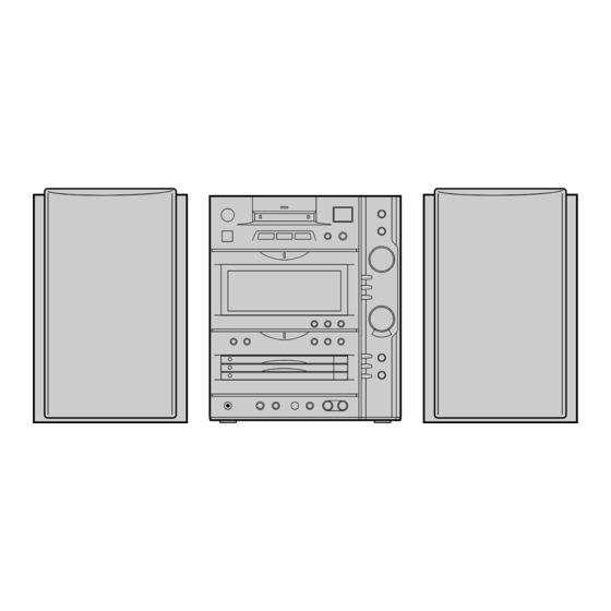
5.Personal Computer Mode Indicator 22 23 24 25 26 27 6.LCD Display 7.Name / TOC-Edit Button: NAME/TOC EDIT 8.Auxiliary Input (Digital/Analog / Phono) Button: AUX MD/CD STEREO MD-X8 POWER 9.Tuner Call (Band Select) Button: TUNER (BAND) 10.3D Surround Indicator CD / MD MD EDIT 11.CD Disc Trays... -
Page 4: Rec Synchro Auto Aux
MD-X8 REMOTE CONTROL 5 6 7 1.Record Mode Button: REC MODE 2.Record Button: 3.Clear Button: CLEAR 4.Program Button: PRGM 5.Play Mode Button: P-MODE 6.Synchro Record Button: SYNCHRO REC SYNCHRO AUTO MARK 7.Auto Mark Button: AUTO MARK MODE 8.Time Display Select Button:TIME... -
Page 5: Operation Manual
MD-X8 OPERATION MANUAL – 5 –... - Page 6 MD-X8 – 6 –...
-
Page 7: Quick Guide
MD-X8 Quick-Guide MD / CD STEREO Guía rápida MD-X8 Turning the Connection Remote control power on and off Conexión Control remoto Conexión y desconexión de la 2 "AA" batteries alimentación Dos pilas "AA" FM Antenna Antena de FM POWER AM Loop Antenna... -
Page 8: Disassembly
MD-X8 DISASSEMBLY STEP REMOVAL PROCEDURE FIGURE Caution on Disassembly Whe disassembling the machine or assenbling it after CD Mechanism 1. Screw ....(U1) x2 10-1 repair, observe the following instructions so as to ensure 2. Top Bord ... (U2) x1 safety and keep its performance. - Page 9 MD-X8 (C2) x1 (C3) x2 (J1) x4 ø3 x8mm (C1) x1 ø3 x8mm (D2) x2 ø3 x10mm (D1) x1 Front Panel Main PWB Sub Chassis Motor M971 (J2) x2 MD Unit ø3 x8mm (D3) x2 (D2) x1 Power PWB ø3 x8mm...
- Page 10 MD-X8 (U3) x1 Push (U1) x2 (U5) x1 ø2 x7mm ø2.6 x12mm Pawl (U6) x1 (U9) x1 Spring (U7) x2 Mechanism ø2 x6mm (U2) x1 Push the pawl of disc tray with a proper screwdriver. (U10) x4 (U8) x1 ø2.6 x10mm...
- Page 11 MD-X8 SPEAKER MD Mechanism Top Panel (A1) x1 Frame Speaker Box Front Panel Figure 11-3 (A4)x1 Front Panel (X1)x4 (A3)x4 Ø4x16mm ø1.7x8.9mm Figure 11-1 (A2)x4 MD Main PWB Speaker Cord Copper foil tape CNS1902 Solder joint (A6)x4 Tweeter Ø3x12mm 24Pin Flat Cable (42)
-
Page 12: Removing And Reinstalling The Main Parts
MD-X8 REMOVING AND REINSTALLING THE MAIN PARTS (A1)x1 MD MECHANISM SECTION ø1.7x5mm Perform steps 1 to 3 of the disassembly method to remove the MD mechanism. (A2) How to remove the magnetic head Soldering x2 (See Fig. 12-1) Magnetic Head 1. - Page 13 MD-X8 How to remove the spindle motor (See Fig. 13-1) 1. Remove the screws (E1) x 3 pcs., and remove the spidle motor. Caution: Be careful so that the turntable is not damaged. Turntable Spindle Motor (E1)x3 Ø1.7x2.5mm Figure 13-1...
-
Page 14: Cd Mechanism Section
MD-X8 CD MECHANISM SECTION (A1) x2 ø2.6 x5mm For the procedure to remove the CD mechanism from the Stop Washer main unit, refer to Disassembling Procedure, Steps 1~10, and (A3) x1 19. (p.8). Pickup How to Remove the optical pickup (See Fig. -
Page 15: Adjustment
MD-X8 ADJUSTMENT TUNER SECTION fL: Low-range frequency • TEST mode setting method fH: High-renge frequency Holding down the ENTER button and TUNER (BAND) button, • AM adjustment and confirmation turn on the power. Frequency is set in the memory (initial AM signal oscillator Frequency 400 Hz, 30%, AM modulation setting) as shown in Table 15. -
Page 16: Cd Test Mode
MD-X8 CD TEST MODE CD test mode setting Any one of test mode can be set by pressing several buttons as follows. Holding down CD PLAY/PAUSE and TACK UP/CUE, turn on POWER. TEST: CD operation test Test Mode Function - CD TEST mode Setting of Test mode Initialization is not performed. - Page 17 MD-X8 MD SECTION • Note Remove the MD unit for repeir, ansd after installing it in the set, be dure to reset it and ascertain that reset has been done. Resetting procedure (1) Unplug the AC cord from the socket, and hold down the RESET buttonm provided at the rear side for more than 10 seconds.
- Page 18 MD-X8 • Test Mode 1. AUTO pre-adjustment mode • Automatic pre-adjustment is performed. (After adjustment the grating adjustment mode is set.) • The adjustment value is output with the aid of system controller interface. 2. AUTO adjustment mode • Automatic adjustment is performed.
- Page 19 MD-X8 2. AUTO adjustment mode Step No. Setting Method Remarks Display Step 1 Testmode STOP state [ t s m Step 2 Press the CD PLAY button two times. AUTO adjustment menu [ A U T O _ A J S T _ ] Step 3 Press once the MD PLAY button.
- Page 20 MD-X8 3. RESULT mode (final adjustment) Step No. Setting Method Remarks Display Step 1 Testmode STOP state [ t s m Step 2 Press the CD PLAY button four times. RESULT menu [ _ R E S U L T _ _ _ ] Step 3 Press once the MD PLAY button.
- Page 21 MD-X8 • If the VOL UP/VOL DOWN button is pressed during setting indication, the setting increases/decreases, and the new setting is stored in RAM. • If the VOL UP/VOL DOWN button is held down, the setting changes continuously with 100 ms cycle.
- Page 22 MD-X8 Setting Method Step No. Remarks Display Step 9 Press once the CD PLAY button. Comparison level setting in case of FOK generation [ F O K L E V f _ (when focus is "ON") Step 10 Press once the CD PLAY button. LPF coefficient setting (normal) in case of FOK generation...
- Page 23 MD-X8 Setting Method Step No. Remarks Display Step 18 Press once the CD PLAY button. TCRS comparison level 1 for high reflection [ T C R S C 1 P _ Step 19 Press once the CD PLAY button. Comparison level in case of COUT generation (playback)
- Page 24 MD-X8 e) TEMP setting Step No. Setting Method Remarks Display Step 1 Testmode STOP state [ t s m Step 2 Press the CD PLAY button seven times. EEPROM setting menu [E E P R O M _ S E T] Step 3 Press once the MD PLAY button.
- Page 25 MD-X8 8. TEST-PLAY mode Step No. Setting Method Remarks Display Step 1 Testmode STOP state [ t s m Step 2 Press the CD MD EDIT button. TEST-PLAY menu [ T E S T _ P L A Y _ ] Step 3 Press once the CD STOP button.
- Page 26 MD-X8 11. EJECT mode Step No. Setting Method Remarks Display Step 1 Testmode EJECT state [ _ _ E J E C T _ _ _ ] Step 2 Press oncethe CD STOP button. Max. power output state [ x p w _ _ _ _ _ _ _ ] Step 3 Press once the CD STOP button.
-
Page 27: Explanation Of Error Display
MD-X8 EXPLANATION OF ERROR DISPLAY Error display Errors Corrective action Can't REC • Defect occurred successively 10 times during REC-PLAY. • Check that the disc is free from flaw, dust • As a result of occurrence of defect during REC-PLAY the and fingerprint. - Page 28 MD-X8 Error display Errors Corrective action BLANK MD • UTOC was read but total TNO and the number of characters of • Perform recording to check that the disc NAME was 0? is recordable disc. DEFECT • Focusing error was caused by shock during REC-PLAY.
- Page 29 MD-X8 -PROM Data List Focus setting Slide setting Setting Item indication Setting Item indication S L G S L 2 F F 1 S L D L I M F F 2 S L D L E V F Z H L E V...
- Page 30 MD-X8 -PROM Setting Mode Chart Figure 30 – 30 –...
-
Page 31: Notes On Schematic Diagram
MD-X8 NOTES ON SCHEMATIC DIAGRAM • Resistor: • The indicated voltage in each section is the one measured by Digital To differentiate the units of resistors, such symbol as K and M are used: the symbol K means 1000 ohm and the symbol M means 1000 Multimeter between such a section and the chassis with no signal kohm and the resistor without any symbol is ohm-type resistor. -
Page 32: Wiring Diagram
MD-X8 MD MAIN PWB-G(BOTTOM) LAMP PWB-C1 MD MECHANISM SWITCH PWB-H CNP741 CNS1901 CNP1904 FW1901 M903 SWITCH A PWB-C2 SWITCH B PWB-C3 LED PWB-C4 FW701 FW701 MD MAIN PWB-G (TOP) MD FLAT CABLE (42) CNS1902 LMP701 CNP12 JOG701 M901 SWITCH C PWB-C5... - Page 33 MD-X8 POWER PWB-B1 CNS1904A CNS1904B BI850 BI830 CNP1904 MD OPTICAL PICK UP UNIT FLEXIBLE PWB T801 POWER TRANSFOMER CNP261 CNS961 M971 FAN MOTOR MAGNETIC HEAD(40) POWER AMP. PWB-B2 CNP1252 CNS1903 IC201 COLOR TABLE BROWN SO201 RD(R) AC POWER ORANGE SUPPLY...
-
Page 34: Block Diagram
MD-X8 Figure 34 BLOCK DIAGRAM (1/4) – 34 –... - Page 35 MD-X8 PICKUP IN SW702A M702 SLED MOTOR M701 SPINDLE MOTOR LASER DRIVER M56748FP FOCUS/TRACKING/ SPIN/SLIDE DRIVER LA9241M SL– SERVO AMP. 27 26 16.934MHz XOUT LC78623D SERVO SIGNAL CAM SWITCH VVDD SWB101 CONTROL SWB102 LVDD SWB103 RVDD SWB104 OPTICAL XVDD PICKUP...
- Page 36 MD-X8 FM/AM Q353 Q354 X351 VOLTAGE CF351 REGURATOR PHASE IF IN Q371 CF352 MONO/ST FM MONO/ST TO µ-COM STEREO FM IN AM IF XT21 AM RF IN T351 AM IN FM IF X352 4.5MHz FM IF IN CF302 VR351 FM MUTE...
- Page 37 MD-X8 IC905 JK902 8 MULTIPLEXER IC751~IC753 74HCU04 DIGITAL 2 INPUT LCD AMP. UNA901 IC752 SO201 DIGITAL 1 CONTROLL JK901 SPEAKER INPUT SO602 BA13058 HEADPHONES TERMINALS AC POWER SUPPLY CORD AC120V 60Hz IC605 TC7WU04F FAN MOTOR M971 ON–OFF FAN MOTOR T801...
-
Page 38: Schematic Diagram / Wiring Side Of P.w.board
MD-X8 MIC PWB-C7 MIC VOLUME VR601 20K(B) IC601 R611 C621 10/50 NO. VOLTAGE D615 R620 R609 1SS133 –11.1V 1.5K C615 R615 Q601 10/50 1.5K KTC3199 GR R603 10.8V MICROPHONE C603 EX_MD-R JK601 220P EX_MD-L C605 R607 220P – TO MAIN PWB... - Page 39 MD-X8 FM SIGNAL AM SIGNAL MAIN PWB-A(1/3) R364 C336 0.022 1.2K C342 C373 R358 R363 0.022 0.018 8.2K 1.2K VR351 AMTRACKING C371 10K(B) 1/50 L353 MUTING FM MUTE LEVEL Q353 C302 R350 KTC3199 GR 0.001 2.7K C332 R365 0.022 C372...
- Page 40 MD-X8 CNP999 MAIN PWB-A(2/3) B A SEL MODE INPUT SELECTOR IC902 IC902 R931 BU2092F C901 100K IC904 NO. VOLTAGE 390P R905 R932 NO. VOLTAGE DATA 4052A 0.2V R1071 SW12 4.7V R906 4052B 4.8V LCK1 SW11 0.2V DUBB MODE SRS PASS/ON R904 4.7V...
- Page 41 MD-X8 R1052 R1051 R1050 220K 2.7K IC901 NO. VOLTAGE C939 R1048 INVERTER 0.01 JK902 IC904 AUX DIGITAL 2 74HC153P INPUT R1049 4.8V ZD901 9 10 11 12 13 14 UZ5.1BSB 0.2V R1053 L905 C945 2.2µH 4.7V 4.8V 0.047 4.7V IC905 4.6V...
- Page 42 MD-X8 23 24 25 MAIN PWB-A(3/3) IC522 FM SIGNAL NO. VOLTAGE CD SIGNAL C541 22/25 –10V R587 100K C573 MIC AMP. R569 IC552 R585 C575 NJM4565D 3.9K Q553 22/50 0.6V – KTC3199 G R551 RMIC MUTE 5.6K C576 22/50 R586 3.9K...
- Page 43 MD-X8 P40 10-H 33 34 D421 1SS133 D422 L421 1SS133 R431 R429 2.2µH L421 2.2µH 2.2K L-CH C429 0.7V 330P R427 AUX OUT L423 100K R419 Q423 2.2µH 5.6K KTC3199 GR R-CH Q541, Q542 : CD MUTE C430 TP39 R428 0.7V...
- Page 44 MD-X8 MAIN PWB-A R1091 R949 R931 R1092 R932 R930 R928 CNP950 R350 R1067 R927 IC902 R1063 R926 Q902 R1039 C372 C367 R925 R924 R362 R1033 R917 C366 R365 C353 IC303 R1064 CNP960 C357 R364 C399 C351 R393 R905 R355 R363...
- Page 45 MD-X8 C331 R350 T302 C367 R349 C366 C353 IC303 R399 R348 L342 R347 C333 C357 3 2 1 C399 C351 C348 R393 Q301 CF302 B C E C346 C334 SO301 C349 C340 R355 C352 C358 R369 R346 C342 CF351 ANTENNA...
- Page 46 MD-X8 NO. VOLTAGE NO. VOLTAGE CD SERVO PWB-C8 2.5V 2.5V DRIVER 2.5V LASER 2.5V 2.6V 47/10 KTA1266 GR 2.5V 4.9V 0.47/50 1.5V 4.9V 2.6V 2.5V 0.33/50 1/50 2.5V 2.5V 4.2V 0.01 2.6V 2.5V 2.6V 2.5V 2.5V 2.5V 4.9V 2.5V VCC1 –...
- Page 47 MD-X8 NO. VOLTAGE 2.5V 2.5V 0.2V 2.5V R77 1K 2.5V R46 1K 2.6V R47 1K 2.6V R45 1K R78 1K CD SIGNAL R48 1K 2.6V 0.01 2.6V 2.5V 2.5V 64 63 62 61 60 59 58 57 56 55 54 53 52 51 50 5.9V...
- Page 48 MD-X8 MOB1 MOB2 MAIN CAM MOTOR TRAY MOTOR M971 FAN MOTOR BIM1 CNS961 TO POWER AMP. PWB TO CD SERVO PWB CNP261 CNP11 COLOR TABLE BROWN R D ( R ) BIM3 SWB101 CAM1 ORANGE TO MAIN PWB YELLOW SWB102 CAM2...
- Page 49 MD-X8 VR602 JK601 VR601 MICROPHONE INPUT LEVEL VOLUME JK901 PC CONTROL HEADPHONES SO602 KEYBORD INPUT SO601 R650 C646 Q601 C639 C650 ZD601 R655 5 6 7 8 1 2 3 4 D615 IC605 R644 R640 2 3 4 4 3 2 1...
- Page 50 MD-X8 DISPLAY PWB- VSS(VD) VOUT VDD PMODE EXA LCD751 VSS CK CKS DISPLAY OSC1 OSC0 R751 680K FROM LCD751 P/S SDA SCL LAMP PWB-C1 BACK LIGHT LMP741 LMP742 LMP743 LMP744 RESB RESET VSS-TEST FROM POWER AMP. PWB BL+B(HIGH) BL_GND CNS830...
- Page 51 MD-X8 PWB-C6 IC751 ~ IC753 : LCD AMP. IC751 BA10358 – TO MAIN PWB – CNP975 P40 1-B IC752 BA10358 R759 150K L751 – 4.7µH RESET TO MAIN PWB D GND CNP970 +13R5V P40 1-C IC753 BA10358 L752 4.7µH –...
- Page 52 MD-X8 LAMP PWB-C1 SWITCH A PWB-C2 LED772 CNP741 R792 SW789 LMP741 MD PLAY/ PAUSE C775 R788 C771 C772 C774 SW788 C773 MD STOP R776 R787 R777 LMP742 R778 VOLUME DOWN JOG701 LMP744 SW787 3D SURROUND R786 SW786 X-BASS LMP743 R785...
- Page 53 MD-X8 SWITCH B PWB-C3 LED PWB-C4 R712 FW701 FW701 LED706 SW701 POWER SW707 COMPUTER NETWORK R706 LED705 RX701 REMOTE SENSOR R714 R711 SW704 SW703 SW702 CD/MD MD EDIT CD/MD MD EDIT CD/MD MD EDIT C701 SW706 TRACK MD EJECT SW705...
- Page 54 MD-X8 FM SIGNAL POWER AMP.PWB-B2 IC201 IC201 STK40705 NO. VOLTAGE – – POWER AMP. –34V –34V Q251 KTC3199 GR –7V 4.5V –5.6V FR202 R205 Q252 R253 KTC3199 GR –34V C205 C221 C250 R201 1/50 C207 4.5V 0.022 100K R245 C203...
- Page 55 MD-X8 Q271,Q272: MOTOR DRIVER RELAY RL201 R271 OUL_L R276 R272 OUL_R D203 ZD271 M971 1SS133 UZ6.2BSB D270 1SS133 MOTOR 4.5V 4.5V D271 R229 1SS133 R275 D201 3.9K 1SS133 Q252 KTC3199 GR Q297 D272 KTC3199 GR 1SS133 4.5V 4.5V D202 C271...
- Page 56 MD-X8 POWER PWB-B1 BI850/CNS850 1 2 3 4 5 6 7 8 C891 C807 D820 R801 D814 D815 C806 C805 D813 D812 F805 1.6A L 250V T801 POWER TRANSFOMER F803 5A L 125V F802 5A L 125V T.F. L801 Figure 56 WIRING SIDE OF P.W.BOARD (7/10)
- Page 57 MD-X8 POWER AMP. PWB-B2 Q871 D871 D872 FR811 R873 C816 BI830/CNS830 R813 RP821 R811 R866 C888 ZD810 C817 R865 C815 R831 C818 C832 Q862 C831 C823 Q851 R820 D801 ZD820 R821 Q850 C820 C851 R853 Q274 CNP261 Q840 Q272 R270...
- Page 58 MD-X8 SITUATION : TP1141 TP1131 C1107 C1111 C1110 0.015 0.0047 0.47 TP1142 C1106 0.47 EFMAGI EFMAGC ADIPI C1119 R1155 330P & ADIPO DIFF ADLPFO DIFF C1102 TP1138 REFI 22KO IC1101 ADIP IR3R55 C1103 RF SIGNAL 22KI REFO PROCESSOR RFADD BIAS...
- Page 59 MD-X8 TP1131 C1107 TP1275 0.0047 TP1142 C1106 0.47 99 98 97 96 9 ADIPI TP1274 EFMMON TP1140 C1119 R1155 AVCC 330P EFMO-I EFMO-I C1202 TP1139 EFMI 99 98 ADIPO AGND AOUT-IN AOUT-IN EOUT-IN EOUT-IN ADLPFO BOUT-IN BOUT-IN TP1138 FOUT-IN 22KO...
- Page 60 MD-X8 SITUATION : Waveforms should be measured by inserting the circuit, as shown in the figure. 100K Connect an oscilloscope. 270P R1211 C1208 0.047 TP1275 TP1210 99 98 97 96 95 94 93 92 91 90 89 88 87 86 85 84 83 82 81 80 79 78 77 76...
- Page 61 MD-X8 MD MAIN PWB-G n in the figure. scilloscope. DADATA ADDATA DFCK BCLK LRCK AND GATE IC1916 74VHC08FT TP1911 R1927 CNP1904 DOUTO TP1901 DIGOUT TO MAIN TP1902 C1951 0.047 CNP961 TP1904 DIGIN P41 12 - B R1974 CNS1904A CNS1904B R1973 6.8K...
- Page 62 MD-X8 SITUATION : CNS1101 FLEXIBLE 9 8 7 5 4 3 2 1 27 26 25 24 23 22 21 20 19 18 17 16 15 14 13 12 11 10 L1251 47uH R1223 C1252 120P C1251 0.027 (CH) EFMO...
- Page 63 MD-X8 VREF3.2V R1401 MINF R1423 HINF TP1405 R1404 C1402 R1424 R1426 0.047 R1472 L1251 47uH R1223 99 98 97 96 95 94 93 92 91 90 89 88 87 86 85 84 83 82 81 TP1260 EFMO XRST DIGCD LDVAR...
- Page 64 MD-X8 SITUATION : IC1990 74AC04FS L1203 4.7µH INVERTOR C1711 0.01 C1716 0.01 28 27 26 25 24 23 22 21 20 REF3.2V IC1701 UDA1340 R1423 A/D,D/A CONVE C1709 0.047 R1424 1 2 3 4 5 6 7 8 9 R1418...
- Page 65 MD-X8 R1712 100K C1711 0.01 C1716 0.01 L3DATA 28 27 26 25 24 23 22 21 20 19 18 17 16 15 MD PLAYBACK SIGNAL IC1701 MD RECORD SIGNAL UDA1340 A/D,D/A CONVERTER 1 2 3 4 5 6 7 8 9...
- Page 66 MD-X8 TO MAIN PWB CNP950 FROM MAGNETIC HEAD CNS1903 MD FLEXIBLE PWB (42) CNS 1902 CNP1252 Q1820 2322 212019181716151413121110 C1251 C1252 R1251 R1827 R1939 R1463 R1459 Q1253 Q1254 C1425 R1461 R1253 C1460 R1734 R1252 R1807 R1223 R1806 IC1251 C1704 Q1804...
- Page 67 MD-X8 • Through-hole where the top, bottom and +B patterns are connected. • Through-hole where the top, bottom and ground patterns are connected. • Through-hole where the top, and bottom patterns are connected. CNS1904A CNS1904B TO MAIN PWB CNP961 JC121...
-
Page 68: Voltage
MD-X8 VOLTAGE (MD MAIN PWB) IC1916 IC1202 Q1801 IC1201 IC1401 IC1601 IC1907 NO. VOLTAGE NO. VOLTAGE NO. VOLTAGE NO. VOLTAGE NO. VOLTAGE NO. VOLTAGE VOLTAGE NO. VOLTAGE 1.58V 1.48V 1.25V 1.1V 2.8V 3.2V 1.1V 2.6V 1.58V 1.6V 0.2V 1.5V 4.9V 3.2V... -
Page 69: Waveforms Of Cd Circuit
MD-X8 WAVEFORMS OF CD CIRCUIT STOP PLAY FOCUS SERCH 0.5ms 0.50 V 10.0 V IC1 20 F.E 0.5ms 10.0 V 0.5ms 5.0 V 0.50 V IC1 54 DRF 0.5ms 1.00 V NORMAL DISC 0.5ms TN0=01 1.00 V 20ms PLAY 1.00 V 0.5ms... -
Page 70: Waveforms Of Md Circuit
MD-X8 WAVEFORMS OF MD CIRCUIT PLAY STATE PIT PLAY Stopped Stopped NORM: 100M S/s NORM: 1M S/s 1997 / 08 / 04 09:30:15 1997 / 08 / 04 13:35:24 CH1 500mV 200mV 500ns/div 1ms/div AC 10:1 DC 10:1 DC 10:1... - Page 71 MD-X8 PLAY Stopped Stopped NORM: 1k S/s NORM: 100M S/s 1997 / 08 / 04 14:19:52 1997 / 08 / 04 11:23:12 1s/div 2us/div DC 10:1 DC 10:1 DC 10:1 DC 10:1 DC 10:1 DC 10:1 DC 10:1 Filter Filter...
-
Page 72: Troubleshooting (Cd Section)
MD-X8 TROUBLESHOOTING (CD SECTION) When the CD does not function When the CD section does not operate When the objective lens of the optical pickup is dirty,this section may not operate.Clean the objective lens,and check the playback operation.When this section does not operate even after the above step is taken,check the following items. - Page 73 MD-X8 • The CD operation keys work. Check the FOCUS-HF system. Playback can be performed without a disc. Focus search OK Does the pickup move up and down two twice? Does the output waveform of IC1 pin 16 (FD) match that Check the area around IC5 to CNP2.
- Page 74 MD-X8 • Check the tracking system. Check the waveform of IC1 pin 7 (TE). The waveform shown in Figure 74-1 Check the periphery of IC1 pin 8 to pin Tracking servo is inoperative. appears, and no disc state appears soon.
- Page 75 MD-X8 • Although HF waveform is normal and time indication is normal, no sound is not output. Check the IC2 pin 48 (EFLG). Usually, the number of pulses of flawless disc is 100 pulses/sec or less. Check the IC2 pin 37 and pin 40.
-
Page 76: Troubleshooting (Md Section)
MD-X8 TROUBLE SHOOTING (MD SECTION) When MD fails to operate If the objective lens of optical pickup is contaminated, MD may fail to operate. At first, clean the objective lens to check playback operation. If MD fails persistently to operate, perform checks as follows. - Page 77 MD-X8 • Disc loading is not normal. Is disc loaded when it is inserted? Check CNP1601 and SW1956. Is the pin 4 of CNP1601 set to L state? Is change observed on the pin 23 or 24 of IC1601? Check IC1401.
- Page 78 MD-X8 • Normal playback When it has been confirmed that EEPROM value is normal in the TEST mode Is initialization performed normally when high reflection disc is Does the playback time display advance? played back? Check IC1201 Does disc rotate normally?
- Page 79 MD-X8 • Record and playback operation Insert the low reflection disc, and after verifying the audio output in the normal mode playback set the record/playback TEST mode Recording from start address cannot be performed. Check whether the disc is record-prohibited.
- Page 80 MD-X8 • Disc motor fails to run Check soldering joint and parts of pins 24 and 25 of IC1201, and Does waveform appear on the pins 24 and 25 of IC1201 in the peripheral circuit. TEST mode focus gain coarse adjustment step?
-
Page 81: Function Table Of Ic
MD-X8 FUNCTION TABLE OF IC IC901 RH-iX2679AFZZ:System Control Micon (iX2679AF) (1/3) Port Name Input/Output Pin No. Terminal Name Function RESET Output Reset signal for MD microcomputer S-ID Output Track mark signal and MD ON/OF control signal for MD LOAD Input... - Page 82 MD-X8 IC901 RH-iX2679AFZZ:System Control Micon(iX2679AF) (2/3) Port Name Input/Output Pin No. Terminal Name Function TRAY SW-A P124 Input Main tray OPEN completion detection switch input H: OPEN completion state when SW is OFF. L: Other state when SW is ON. This switch provides the CLOSE function when the tray lid is pressed.
- Page 83 MD-X8 IC901 RH-iX2679AFZZ:System Control Micon(iX2679AF) (3/3) Port Name Input/Output Pin No. Terminal Name Function COIN Output Serial output of command data to CD DSP CQCK SCK0 Output Serial clock output to CD DSP Output Reset output to CD DSP element...
- Page 84 MD-X8 IC901 RH-iX2679AFZZ:System Control Micon(iX2679AF) MIC detection and DSTB port replacement (EX MD) SW1 DUBB MODE (EX MD) SW2 STOP DSTB input must be through INTP6 interruption port. (EX MD) SW3 SKIP +1 P06->INTP6; MIC detection -> (MD)DST (EX MD) SW4 SKIP +10...
- Page 85 MD-X8 IC1101 VHiiR3R55//-1:RF Signal Processor (IR3R55) Function Terminal Name Pin No. RF signal input terminal 1 Input of RF signal output of pickup RF signal input terminal 2 Input of RF signal output of pickup RF signal input terminal 3 Input of RF signal output of pickup...
- Page 86 MD-X8 IC1201 VHiLR37648/-1:ENDEC (LR37648) (1/2) Function Terminal Name Input/Output Pin No. EFMMON Output EFM monitor output AVCC — Analog power EFMI Input EFM signal input from RF amp. AGND — Analog GND Input Focus error signal A Input Tracking error signal E...
- Page 87 MD-X8 IC1201 VHiLR37648/-1:ENDEC (LR37648) (2/2) Function Terminal Name Input/Output Pin No. TESO1 Output PLLLR. Microcomputer extension output port 2 in case of selection TESO3 In/Output PLLOSC. Microcomputer extension output port 3 in case of selection TEST4 In/Output EXTCLK. Microcomputer extension output port 4 in case of selection...
- Page 88 MD-X8 IC1401 RX-iX0227AWZZ:MD System Micon Control (IX0227AW) (1/2) Function Terminal Name Input/Output Pin No. P96/ANEX1 Output Input/Output it port P96 P95/ANEX0 Output Input/Output it port P96 P94/DA1 Output LDVAR (laser power adjustment output) P93/DA0 Output ADJS (for automatic adjustment step check)
- Page 89 MD-X8 IC1401 RX-iX0227AWZZ:MD System Micon Control (IX0227AW) (2/2) Function Terminal Name Input/Output Pin No. P42/A18 In/Output SYS D2 (data bus 2) P41/A17 In/Output SYS D1 (data bus 1) P40/A16 In/Output SYS D0 (data bus 0) P37/A15 Output Input/Output it port P37...
- Page 90 MD-X8 IC1101 VHiiR3R55//-1:RF Signal Processor (IR3R55) ADIPI ADIPO DIFF DIFF ADLPFO ADIP REFI 22KO REFO 22KI BIAS RFADD TCGI TCGO AOUT BOUT EOUT LOGIC FOUT Figure 90-1 BLOCK DIAGRAM OF IC IC1201 VHiLR37648/-1:ENDEC (LR37648) 75 74 73 72 71 70 69 68 67 66 65 64 63 62 61 60 59 58 57 56 55 54 53 52 51...
-
Page 91: Parts Guide
“HOW TO ORDER REPLACEMENT PARTS” To have your order filled promptly and correctly, please furnish the For U.S.A. only following information. Contact your nearest SHARP Parts Distributor to order. 1. MODEL NUMBER 2. REF. No. 3. PART NO. 4. DESCRIPTION For location of SHARP Parts Distributor, Please call Toll-Free;... - Page 92 MD-X8 PRICE PRICE DESCRIPTION PART CODE PARTS CODE DESCRIPTION RANK RANK INTEGRATED CIRCUITS Q841 VS2SD2012//-1 AD Silicon,NPN,2SD2012 Q850 VSKTC3199GR-1 AB Silicon,NPN,KTC3199 GR VHILA9241M/-1 AS Servo Amp.,LA9241M Q851 VS2SD2012//-1 AD Silicon,NPN,2SD2012 VHILC78623D-1 AY Servo/Signal Control,LC78623D Q860 VSKTC3199GR-1 AB Silicon,NPN,KTC3199 GR VHIM56748FP-1...
- Page 93 MD-X8 PRICE PRICE PART CODE DESCRIPTION PARTS CODE DESCRIPTION RANK RANK AB 4.7 µF,25V,Electrolytic T801 RTRNP0169AWZZ J BT Power RC-EZY475AF1E AA 0.022 µF,25V VCTYMN1EF223Z COILS AB 0.1 µF,16V VCTYPA1CX104K AA 0.022 µF,25V VCTYMN1EF223Z AC 0.82 µH AB 100 µF,10V,Electrolytic VP-XHR82K0000 RC-EZY107AF1A AE 3 µH,Trap...
- Page 94 MD-X8 PRICE PRICE DESCRIPTION PART CODE PARTS CODE DESCRIPTION RANK RANK AB 1 µF,50V,Electrolytic C393 RC-GZA105AF1H C701 VCKYMN1HB101K J AA 100 pF,50V AB 47 µF,16V,Electrolytic AB 1 µF,50V,Electrolytic C394 RC-GZA476AF1C C702 RC-GZA105AF1H AA 0.022 µF,25V C395 VCTYMN1EF223Z C703 VCKYMN1HB101K J AA 100 pF,50V AB 100 µF,10V,Electrolytic...
- Page 95 MD-X8 PRICE PRICE DESCRIPTION PARTS CODE DESCRIPTION PART CODE RANK RANK AA 0.0047 µF,50V C1107 VCKYTV1HB472K VRD-SA2CD0R0J AB 0 ohm,Jumper,ø1.9×3.4mm,Red AD 1 µF,6.3V C1109 VCKYTV0JB105K VRD-ST2CD0R0J AA 0 ohm,1/6W,Jumper AC 0.47 µF,16V C1110 VCKYTV1CB474K VRS-CY1JB000J AA 0 ohm,Jumper,0.8×1.55mm, AA 0.015 µF,50V...
- Page 96 MD-X8 PRICE PRICE DESCRIPTION PART CODE PARTS CODE DESCRIPTION RANK RANK R227,228 VRD-ST2EE4R7J AA 4.7 ohms,1/4W R453,454 VRD-ST2CD222J AA 2.2 kohms,1/6W R229,230 VRD-ST2CD563J AA 56 kohms,1/6W R455~458 VRD-MN2BD392J AA 3.9 kohms,1/8W R239,240 VRD-ST2EE331J AA 330 ohms,1/4W R459 VRD-ST2CD103J AA 10 kohm,1/6W...
- Page 97 MD-X8 PRICE PRICE PART CODE DESCRIPTION PARTS CODE DESCRIPTION RANK RANK R751 VRD-MN2BD684J AA 680 kohms,1/8W R957 VRD-ST2CD102J AA 1 kohm,1/6W R752 VRD-ST2CD104J AA 100 kohm,1/6W R958 VRD-MN2BD103J AA 10 kohm,1/8W R753 VRD-ST2CD124J AA 120 kohms,1/6W R959 VRD-ST2CD102J AA 1 kohm,1/6W...
- Page 98 MD-X8 PRICE PRICE DESCRIPTION PART CODE PARTS CODE DESCRIPTION RANK RANK R1409 VRS-CY1JB102J AA 1 kohm,1/16W R1927 VRS-TV2AB220J AA 22 ohms,1/10W R1412 VRS-CY1JB104J AA 100 kohm,1/16W R1939 VRS-CY1JB102J AA 1 kohm,1/16W R1413 VRS-CY1JB332J AA 3.3 kohms,1/16W R1947 VRS-TV2AB470J AA 47 ohms,1/10W...
- Page 99 MD-X8 PRICE PRICE PART CODE DESCRIPTION PARTS CODE DESCRIPTION RANK RANK CNS2A/B QCNWN0859AWZZ J AF Connector Ass’y,7/7Pin SW784 QSW-K0005AWZZ J AC Switch,Key Type CNS3A/B QCNWN0857AFZZ J AK Connector Ass’y,6/6Pin [Multi Control Up] CNS950/A/B QCNWN0959AWZZ J AS Connector Ass’y,8/2/6Pin SW785 QSW-K0005AWZZ J...
- Page 100 MD-X8 PRICE PRICE DESCRIPTION PART CODE PARTS CODE DESCRIPTION RANK RANK M903 RMOTV0014AWM1 J AQ MD Loading Motor Ass’y SWB108 QSW-P0920AFZZ AC Switch,Push Type [CD Set] SW1952A/B QSW-P0006AWZZ J AG Switch,Push Type CABINET PARTS [Write Pro/Direct] SW1953 QSW-M0157AFZZ AD Switch,Push Type [Lead In]...
- Page 101 MD-X8 PRICE PRICE PART CODE DESCRIPTION PARTS CODE DESCRIPTION RANK RANK MSPRD0108AWFJ J AC Spring,Fan Motor NBRGC0003AWZZ J AC Bearing Metal LX-BZ0880AFZZ AC Screw,ø2×2mm XBPSD30P10KS0 AA Screw,ø3×10mm XEBSD26P10000 AA Screw,ø2.6×10mm XEBSD30P10000 AA Screw,ø3×10mm LX-HZ0087AFFD AA Screw,ø3×8mm XWHSD32-10130 AA Washer,ø3.2×ø13×1.0mm XJBSF30P08000 AA Screw,ø3×8mm...
- Page 102 MD-X8 CNS1903 SW1956 PWB-H SW1953 1952A/B SW1955 SW1954 603x2 FW1901 CNS1904 603x2 PWB-G 612x4 M902 M903 M901 606x3 Figure 11 MD MECHANISM EXPLODED VIEW – 11 –...
- Page 103 MD-X8 306-2 306-1 306-3 703x2 M701 M702 305x2 SW702A PWB-D Figure 12 CD MECHANISM EXPLODED VIEW – 12 –...
- Page 104 MD-X8 CD Mechanism 805x4 803x2 804x3 104 105 801x2 111x2 110x2 108x3 108x3 SWB101 PWB-F ~104 MOB1 108x3 123x4 MOB2 80mm Figure 13 CHANGER MECHANISM EXPLODED VIEW – 13 –...
- Page 105 MD-X8 PWB-B3 MD Mechanism Unit 610x2 602x2 M971 611x5 604x6 PWB-C4 606x2 PWB-C3 604x3 261x2 263x2 601x2 609x2 262x2 PWB-C6 602x2 604x7 604x2 JOG701 604x10 PWB-C5 LCD751 611x2 PWB-C1 611x2 PWB-C2 604x2 603x2 201-17 201-11 201-19 201-14 Silicon 201-12 617x2...
- Page 106 MD-X8 TWEETER SP3 (L-CH) SP4 (R-CH) 3.3µF, 100V, Film Capacitor WOOFER SP1 (L-CH) SP2 (R-CH) 912x2 SPEAKER TERMINAL (905) SP3 (L-CH) SP4 (R-CH) 911x4 910x4 906x4 TWEETER SP3 (L-CH) SP4 (R-CH) SPEAKER SP1 (L-CH) TERMINAL WOOFER (905) SP2 (R-CH) SP1 (L-CH)
- Page 107 MD-X8 PACKING OF THE SET SSAKH0022AWZZ SPAKA0133AWZZ Polyethylene Bag, Unit L Mark Packing Add., Left/Right TLABN0001AWZZ Label, Serial Month AM Loop Antenna R Mark FM Antenna Speaker Cord Operation 92L411-0086 Manual 92L412-0088 Polyethylene Bag, Recording Front Remote Control Packing Add.,...
- Page 108 MD-X8 © COPYRIGHT 1997 BY SHARP COPORATION ALL RIGHTS RESERVED. No part of this publication may be reproduced, stored in a retrieval system, or transmitted in any from or by any means, electronic, mechanical, photocopying, recording, or otherwise, without prior written permission of the publisher.
Need help?
Do you have a question about the MD-X8 and is the answer not in the manual?
Questions and answers