Table of Contents
Advertisement
Quick Links
GUITAR PRE-AMPLIFIER
SERVICE MANUAL
CONTENTS
SPECIFICATIONS·············································································· 3
PANEL LAYOUT················································································· 4
CIRCUIT BOARD LAYOUT ······························································ 5
BLOCK DIAGRAM·············································································· 6
DISASSEMBLY PROCEDURE ························································ 7
LSI PIN DESCRIPTION····································································· 9
IC BLOCK DIAGRAM ······································································ 12
CIRCUIT BOARDS··········································································· 14
TEST PROGRAM············································································· 18
ERROR MESSAGES······································································· 21
MIDI IMPLEMENTATION CHART················································· 22
PARTS LIST
OVERALL CIRCUIT DIAGRAM
GA
011400
HAMAMATSU, JAPAN
19980301-198000
2.1K-656
Printed in Japan '98.03
Advertisement
Table of Contents

Related Manuals for Yamaha DG 100-212


Summary of Contents for Yamaha DG 100-212
- Page 1 GUITAR PRE-AMPLIFIER SERVICE MANUAL CONTENTS SPECIFICATIONS·············································································· 3 PANEL LAYOUT················································································· 4 CIRCUIT BOARD LAYOUT ······························································ 5 BLOCK DIAGRAM·············································································· 6 DISASSEMBLY PROCEDURE ························································ 7 LSI PIN DESCRIPTION····································································· 9 IC BLOCK DIAGRAM ······································································ 12 CIRCUIT BOARDS··········································································· 14 TEST PROGRAM············································································· 18 ERROR MESSAGES······································································· 21 MIDI IMPLEMENTATION CHART·················································...
-
Page 2: Specifications
IMPORTANT NOTICE This manual has been provided for the use of authorized Yamaha Retailers and their service personnel. It has been assumed that basic service procedures inherent to the industry, and more specifically Yamaha Products, are already known and understood by the users, and have therefore not been restated. -
Page 3: Specifications
DG100-212 SPECIFICATIONS Digital Section Connection Jacks Complete Digital Signal Processing INPUT HIGH/LOW, SPEAKER, EFFECT SEND/RETURN: Internal 8 Channel Preset Standard Phone Mono Jack Digital Reverb (SPRING, HALL, PLATE) LINE OUT: Cannon Jack Digital Tape Echo MIDI IN, MIDI OUT: 5 pin DIN Speaker Simulator (LINE OUT) A/D Converter 20 bit... -
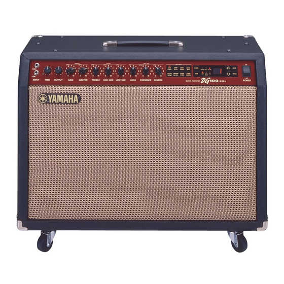
Page 4: Panel Layout
DG100-212 PANEL LAYOUT Front panel Input Jack (INPUT HIGH, LOW) Trim Control (TRIM) Output Level Control (OUTPUT) Gain Volume (GAIN) Master Volume (MASTER) Tone Controls (TREBLE, HIGH MID, LOW MID, BASS, PRESENCE) Reverb Volume (REVERB) Amp Select Button/Amp Select Display (LEAD 1, 2/DRIVE 1, 2/CRUNCH 1, 2/CLEAN 1, 2) Reverb Type Select Button (REVERB) Reverb Type Display Lamp (SPRING, HALL, PLATE) -
Page 5: Circuit Board Layout
DG100-212 CIRCUIT BOARD LAYOUT MAIN 5/5 MAIN 4/5 MAIN 3/5 MAIN 2/5 AC cord CN404 CN316 CN310 CN317 CN315 CN402 CN401 CN403 CN314 CN302 CN102 CN313 CN312 CN301 Power MAIN 1/5 CN304 Transformer K304 CN309 CN303 CN101 K303 CN307 CN308 K302 K301 CN318... -
Page 6: Block Diagram
DG100-212 BLOCK DIAGRAM DISASSEMBLY PROCEDURE Pre-Main Unit 1-1 Remove the four (4) screws marked [70A]. The back board (U) can then be removed. (Fig. 1) 1-2 Remove the plug of the connector assembly (speaker) located on the rear panel and the six (6) screws marked [30A]. -
Page 7: Ground
DG100-212 Front Panel Assembly 3-1 Remove the pre-main unit. (See Procedure 1) 3-2 Remove the five (5) screws marked [30B]. The front panel assembly can then be removed. (Fig. 3) ANR Circuit Board 4-1 Remove the pre-main unit. (See Procedure 1) 4-2 Remove the screw marked [50], the two (2) screws marked [170], the two (2) knobs marked [60] and the four (4) hexagonal nuts marked [A]. - Page 8 DG100-212 PN Circuit Board 11. VR Circuit Board 8-1 Remove the pre-main unit. (See Procedure 1) 11-1 Remove the pre-main unit. (See Procedure 1) 8-2 Remove the front panel assembly. (See 11-2 Remove the front panel assembly. (See Procedure 3) Procedure 3) 8-3 Remove the ten (10) screws marked [80B].
-
Page 9: Lsi Pin Description
DG100-212 LSI PIN DESCRIPTION HD6413002FP16 (XQ375A00) CPU <H8/3002> NAME FUNCTION NAME FUNCTION Port A Address bus Power supply Address bus Port B Ground P60//WAIT PB6//DREQ0 P61//BREQ Port 6 PB7//DREQ1 /RESO Reset P62//BACK Ground ø øout P90/TXD0 Transmit data (MIDI OUT) /STBY Stand-by mode signal P91/TXD1... - Page 10 DG100-212 YSS228D-F (XQ962D00) DSP3 (Digital Signal Processor) NAME FUNCTION NAME FUNCTION Ground Ground DB13 System master clock input (60M or30MHz) DB14 System master clock input (60M or30MHz) Power supply DB15 /SYNCI System synch. input DB16 /SYNCO System synch. output DB17 System clock input (30MHz) DB18 System clock output (30MHz)
- Page 11 DG100-212 YSF210-M (XK280A00) Digital Filter NAME FUNCTION NAME FUNCTION OBIT1 Output bit selection System clock OBIT2 22 bit 20 bit 18 bit no output VSS2 Ground OBIT 1 OBIT 2 Bit clock SDSY L/R select and input timing No connection IBIT1 Input bit selection Synchronous/Asynchronous system clock...
-
Page 12: Ic Block Diagram
DG100-212 IC BLOCK DIAGRAM TCHCU04AF-TP1(XD660A00) SN74HC08NSR (XD831A00) TC74VHC32F (XN963A00) Hex Inverter Quad 2 Input AND Quad 2 Input OR TC74HC157AF-TP1 XH603A00 TC74HC164AF (XQ967A00) TC74HC175AF -TP1(XD658A00) Quad 2 to 1 Multiplexer 8-Bit Shift Register Quad D-Type Flip-Flop SELECT SIRIAL INPUT STROBE Q CL OUTPUTS OUTPUTS... - Page 13 DG100-212 NE5532P(IG102500) NJM072D(IG107000) Dual Operational Amplifier Dual Operational Amplifier +DC Voltage Output A Supply Inverting Output B Input A Inverting Non-Inverting Input B Input A Non-Inverting -DC Voltage Supply Input B MB3790PF(XR967A00) ASSP CONTROL 590k Reference 2.65V Voltage ALARM1 1.24V Power Supply Circuit 3µA...
-
Page 14: Circuit Boards
DG100-212 CIRCUIT BOARDS DM Circuit Board MIDI to DM-CN9 Component side Note : See parts list for details of circuit board component parts. ENA-VZ77180-1/9... - Page 15 DG100-212 DM Circuit Board to DM-CN9 Pattern side Note : See parts list for details of circuit board component parts. ENA-VZ77180-1/9...
- Page 16 DG100-212 PN Circuit Board Panel Layout Component side Pattern side VR Circuit Board Note : See parts list for details of circuit board component parts. GAIN MASTER TREBLE HIGH MID LOW MID BASS PRESENCE REVERB TIME FEED BACK LEVEL PN : ENA-VZ77230-1/4 Component side VR : CNA-VZ89700-1/10...
- Page 17 DG100-212 MAIN Circuit Board ANR Circuit Board LINE OUT EFFECT LINE OUT SEND RETURN BLEND LEVEL Component side ANF2 Circuit Board ANF Circuit Board Component side HIGH Note : See parts list for details of circuit board Component side component parts. TRIM OUTPUT INPUT...
-
Page 18: Test Program
DG100-212 TEST PROGRAM The LED Check is finished and the DG100-212 E0 ~ E3 A. SET-UP E. TEST PROGRAM selects the next test no., so the LED shows a "1". If a Motor Drive Volume Check operation has 1. If no specific frequency is required, set the test (Relay Check) not been finished in 20 seconds, the LED display (Error Number) - Page 19 DG100-212 (Test Contents) (Test Contents) The RAM Backup Battery check is executed The Flash Memory Erase/Write check is executed automatically. automatically. When all the LEDs light simultaneously, the When the check is started, the LED display shows Battery Check is finished. Then the DG100-212 from "70"...
- Page 20 DG100-212 (Test Contents) The DG100-212 sets the conditions for the signal Sound Check through the analogue circuit, the A/D converter, the DSP-3 and the D/A Converter. When the Sound Check is started, the LED display shows "81". The Sound Check has two conditions. If the RECALL key is pressed when the LED display shows "81", the LED display changes to "82"...
-
Page 21: Error Messages
Backup battery power is depleted. SOLUTION: Continued use of the device will result in the loss of data. Return the device to the music dealer where you purchased it or, the nearest Yamaha Service center and have the battery replaced. -
Page 22: Midi Implementation Chart
DG100-212 YAMAHA [ Digital Guitar Amplifier ] Date:24-Dec-1997 Model DG100-212 MIDI Implementation Chart Version : 1.0 +----------------------------------------------------------------------+ Transmitted Recognized Remarks Function ... : :-------------------+----------------+----------------+----------------: :Basic Default : 1 - 16, off : memorized :Channel Changed : 1 - 16, off... -
Page 23: Parts List
DG100-212 OVERALL CIRCUIT DIAGRAM 1/2 DM,ANR DG100-212 ASSP Photo Coupler SRAM SRAM DATA SELECTOR DSP3 to PN-CN202 to VR-CN603 BUS BUFFER DRAM BUS BUFFER to PN-CN201 to MAIN1/5-CN308 DSP3 DRAM D-FF D-FF to VR-CN602 to VR-CN604 REGULATOR OP AMP to ANF-CN501 OP AMP REGULATOR COUNTER... -
Page 24: Parts List
DG100-212 OVERALL CIRCUIT DIAGRAM 2/2 (MAIN1/5~5/5,PN,VR,ANF,ANF2) DG100-212 to DM-CN4 to DM-CN5 ANF2 TAPE HIGH UTIL ECHO MOTOR DRIVER OP AMP LEAD1,LEAD2,DRIVE1,DRIVE2 CRUNCH1,CRUNCH2,CLEAN1,CLEAN2 ,STORE,RECALL D-FF SPRING HALL PLATE GAIN MASTER TREBLE HIGH MID LOW MID BASS PRESENCE REVERB (TIME) (FEED BACK) (LEVEL) KEC-54163-5/5 MODE,RE VERB... -
Page 25: Table Of Contents
GUITAR AMPLIFIER PARTS LIST CONTENTS OVERALL ASSEMBLY····································································································································· 2 PRE-MAIN UNIT················································································································································ 4 OVERALL CABINET ASSEMBLY ·················································································································· 6 FRONT PANEL ASSEMBLY ··························································································································· 7 CHASSIS ASSEMBLY······································································································································ 8 ELECTRICAL PARTS ································································································································ 9~18 Notes : DESTINATION ABBREVIATIONS : Japanese model : Australian model U : U.S.A. model : European model C : Canadian model D : German model... -
Page 26: Overall Assembly
DG100-212 OVERALL ASSEMBLY Pre-main unit; See page 4 Overall cabinet assembly; See page 6... - Page 27 DG100-212 PART NO. DESCRIPTION REMARKS REF NO. RANK OVERALL ASSEMBLY DG100-212 Pre-main Unit (VZ74050) Pre-main Unit (VZ74060) Pre-main Unit (VZ74800) Pre-main Unit (VZ74810) VZ893900 OVERALL CABINET ASSEMBLY VP104600 Oval Head Screw 5.0X35 MFC2BL EW300020 Washer 5S MFC2BL XU436A00 Speaker VINTAGE30 EX000990 Hexagonal Nut 5.0 MFZN2BL...
-
Page 28: Pre-Main Unit
DG100-212 PRE-MAIN UNIT AC cord assembly Power transformer Earth mark ANR circuit board assembly Chassis assembly; See page 8 Front panel assembly; See page 7 Power switch assembly... - Page 29 DG100-212 PART NO. DESCRIPTION REMARKS REF NO. RANK PRE-MAIN UNIT DG100-212 Pre-main Unit (VZ74050) Pre-main Unit (VZ74060) Pre-main Unit (VZ74800) Pre-main Unit (VZ74810) Front Panel Assembly (VZ74040) Front Panel Assembly (V001390) Front Panel Assembly (V001400) Front Panel Assembly (V001410) Chassis Assembly (VZ74020) Chassis Assembly (VZ74030)
-
Page 30: Overall Cabinet Assembly
DG100-212 OVERALL CABINET ASSEMBLY Handle assembly Front board assembly PART NO. DESCRIPTION REMARKS REF NO. RANK VZ893900 OVERALL CABINET ASSEMBLY DG100-212 Cabinet Assembly (VZ89410) Vinyl 122KURO 9A (VZ89440) AA809050 Corner EX802320 Round Head Wood Screw 3.5X16 FNM33G NB812640 Handle Assembly VZ894500 Front Board Assembly V2237300... -
Page 31: Front Panel Assembly
DG100-212 FRONT PANEL ASSEMBLY VR circuit board assembly 70 j PN circuit board assembly 70 g REMARKS PART NO. DESCRIPTION REF NO. RANK Front Panel Assembly DG100-212 J (VZ74040) Front Panel Assembly DG100-212 U (V001390) Front Panel Assembly DG100-212 E (V001400) Front Panel Assembly DG100-212 B... -
Page 32: Chassis Assembly
DG100-212 CHASSIS ASSEMBLY... - Page 33 DG100-212 PART NO. DESCRIPTION REMARKS REF NO. RANK Chassis Assembly DG100-212 J (VZ74020) Chassis Assembly DG100-212 U (VZ74030) Chassis Assembly DG100-212 E (VZ74780) Chassis Assembly DG100-212 B (VZ74790) VZ735800 Chassis VZ771800 Circuit Board (XU331B0) EP600230 Bind Head Tapping Screw-B 3.0X6 MFZN2BL EP600190 Bind Head Tapping Screw-B 3.0X8 MFZN2BL...
-
Page 34: Electrical Parts
DG100-212 ELECTRICAL PARTS PART NO. DESCRIPTION REMARKS REF NO. RANK ELECTRICAL PARTS DG100-212 VZ771800 Circuit Board (XU331B0) VZ974000 Circuit Board MAIN (XU365B0) VZ975900 Circuit Board MAIN (XU365B0) VZ976300 Circuit Board MAIN (XU365B0) VZ974200 Circuit Board (XU365B0) VZ974600 Circuit Board (XU365B0) V2156100 Circuit Board ANF2... - Page 35 DG100-212 PART NO. DESCRIPTION REMARKS REF NO. RANK C118 UA353680 Mylar Capacitor 6800P 50V J C119 VD930900 Semiconductive Cera. Cap. 0.1000 25V M C120 UB245100 Monolithic Ceramic Cap. F 0.100 25V Z C121 VD534400 Monolithic Ceramic Cap. 1.500 25V Z C122 VD930900 Semiconductive Cera.
- Page 36 DG100-212 PART NO. DESCRIPTION REMARKS REF NO. RANK IC008 XU462A00 MSM514260C-60TS-K DRAM 4M IC008 XT776A00 UPD424260G5-70-7JF DRAM 4M IC011 XU462A00 MSM514260C-60TS-K DRAM 4M IC011 XT776A00 UPD424260G5-70-7JF DRAM 4M IC012 XS544A00 W24257S-70LL SRAM 256K IC013 XQ375A00 HD6413002FP16 IC014 XS544A00 W24257S-70LL SRAM 256K IC018 XH603A00 TC74HC157AF-TP1...
- Page 37 DG100-212 PART NO. DESCRIPTION REMARKS REF NO. RANK R129 HF755820 Carbon Resistor 820.0 1/4 J R130 HF755820 Carbon Resistor 820.0 1/4 J R131 HF756470 Carbon Resistor 4.7K 1/4 J R132 HF756470 Carbon Resistor 4.7K 1/4 J R133 HF756220 Carbon Resistor 2.2K 1/4 J -138 HF756220...
- Page 38 DG100-212 PART NO. DESCRIPTION REMARKS REF NO. RANK C408 UA355100 Mylar Capacitor 0.1000 50V J C409 UR847100 Electrolytic Cap. 10.00 25.0V C410 FG652100 Ceramic Capacitor-SL 100P 50V J C411 UR847330 Electrolytic Cap. 33.00 25.0V C412 UR847100 Electrolytic Cap. 10.00 25.0V C413 FG613100 Ceramic Capacitor-B...
- Page 39 DG100-212 PART NO. DESCRIPTION REMARKS REF NO. RANK CN404 LB918040 Base Post Connector XH- 4P TE CN501 Shield Wire 3P L=250 B&C (VZ97570) CN502 Shield Wire 2P L=100 B&C (VZ97550) CN503 LB918050 Base Post Connector XH- 5P TE CN504 VB390200 Connector Base Post PH- 6P TE CN601...
- Page 40 DG100-212 PART NO. DESCRIPTION REMARKS REF NO. RANK R309 HF755220 Carbon Resistor 220.0 1/4 J R310 HF758100 Carbon Resistor 100.0K 1/4 J R311 HF756390 Carbon Resistor 3.9K 1/4 J R312 HF758100 Carbon Resistor 100.0K 1/4 J -315 HF758100 Carbon Resistor 100.0K 1/4 J R316 HF757220...
- Page 41 DG100-212 PART NO. DESCRIPTION REMARKS REF NO. RANK R508 HF757150 Carbon Resistor 15.0K 1/4 J R509 HF758100 Carbon Resistor 100.0K 1/4 J R510 HF757330 Carbon Resistor 33.0K 1/4 J R511 HF758100 Carbon Resistor 100.0K 1/4 J R512 HF758100 Carbon Resistor 100.0K 1/4 J R513 HF756330...
- Page 42 DG100-212 REMARKS PART NO. DESCRIPTION REF NO. RANK VR610 VU647600 Motor Drive Volume RK16812MG 10KB BASS VR611 VA788500 Trimmer Potentiometer B 220.0K 3P RHE VR612 VU647600 Motor Drive Volume RK16812MG 10KB PRESENCE VR613 VU647600 Motor Drive Volume RK16812MG 10KB REVERB ZD301 VQ554700 Zener Diode...
Need help?
Do you have a question about the DG 100-212 and is the answer not in the manual?
Questions and answers