Yamaha P-85 Service Manual
Digital piano
Hide thumbs
Also See for P-85:
- Owner's manual (38 pages) ,
- Quick operation manual (2 pages) ,
- Quick operation manual (2 pages)
Table of Contents
Advertisement
CL
001792
P-85: 200710
P-85S: 200710
SERVICE MANUAL
SERVICE MANUAL
CONTENTS
Midi Implementation Chart ...........................................47
Midi Data Format ...............................................................48
Copyright (c) Yamaha Corporation. All rights reserved. PDF
.................................................3
......................................4
.................5
..............................6
.............................19
..................................21
.......................................22
.............................31/35
...........39/43
HAMAMATSU, JAPAN
P-85
P-85S
'07.10
&
Advertisement
Table of Contents

Related Manuals for Yamaha P-85


Summary of Contents for Yamaha P-85
- Page 1 CIRCUIT BOARDS ........22 TEST PROGRAM ......31/35 DATA BACKUP ...39/43 MIDI IMPLEMENTATION CHART ...........47 MIDI DATA FORMAT ...............48 PARTS LIST BLOCK DIAGRAM CIRCUIT DIAGRAM 001792 HAMAMATSU, JAPAN P-85: 200710 P-85S: 200710 Copyright (c) Yamaha Corporation. All rights reserved. PDF ’07.10 &...
- Page 2 IMPORTANT NOTICE This manual has been provided for the use of authorized Yamaha Retailers and their service personnel. It has been assumed that basic service procedures inherent to the industry, and more specifically Yamaha Products, are already known and understood by the users, and have therefore not been restated.
-
Page 3: Specifications
When an optional FC3 Foot Pedal or an optional LP-5 Pedal Unit is connected, the half pedal effect can be used. Specifi cations and descriptions in this owner’s manual are for information purposes only. Yamaha Corp. reserves the right to change or modify products or specifi... -
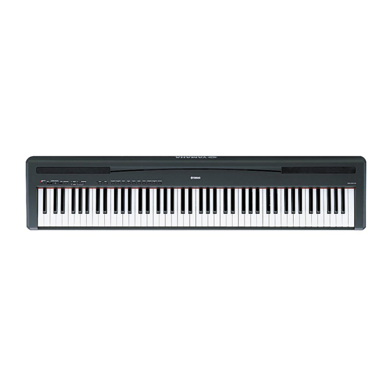
Page 4: Panel Layout
P-85/P-85S PANEL LAYOUT Shows the jacks Shows the jacks and terminals as and terminals as seen when viewed seen when viewed from the rear of from the rear of the instrument. the instrument. q [STANDBY/ON] switch w [MASTER VOLUME] slider... -
Page 5: Circuit Board Layout
P-85/P-85S CIRCUIT BOARD LAYOUT <Bottom view> Upper case assembly Lower case assembly <Top view> Speaker L Speaker R GHL88L GHL88M <Top view> GHL88H Keyboard assembly... -
Page 6: Disassembly Procedure
P-85/P-85S DISASSEMBLY PROCEDURE Caution: Be sure to attach the removed fi lament tape just as it was before removal. Pay attention not to insert and install the cable to the connector inversely. (Photo 1) Photo 1 Front Side (Printed Side) - Page 7 P-85/P-85S DM Circuit Board (Time required: About 11 minutes) Remove the lower case assembly. (See procedure 1.) Remove the four (4) screws marked [30A]. The DM circuit board can then be removed. (Fig. 2) AM Circuit Board (Time required: About 12 minutes) Remove the lower case assembly.
- Page 8 P-85/P-85S Keyboard Assembly (Time required: About 13 minutes) Remove the lower case assembly. (See procedure 1.) Remove the eight (8) screws marked [30E] and eight (8) screws marked [31]. The keyboard assembly can then be removed. (Fig. 3) Keyboard assembly <Bottom view>...
- Page 9 P-85/P-85S PN2 Circuit Board (Time required: About 14 minutes) Remove the lower case assembly. (See procedure 1.) Remove the keyboard assembly. (See procedure 7.) Remove the ten (10) screws marked [30G]. The PN2 circuit board can then be removed. (Fig. 5)
- Page 10 P-85/P-85S Pedal Assembly, PEDAL Circuit Board (Time required: About 4 minutes) 11-1 Disconnect the PK cable from the [PEDAL UNIT] jack. (Fig. 6) 11-2 Tilt the keyboard stand backward to lift the forward bottom portions and remove the pedal assembly.
- Page 11 P-85/P-85S 11-6 Rotate and remove the three (3) pedal pieces from the lower pedal case. (Fig. 10) 11-7 Remove the six (6) screws marked [90]. The PEDAL circuit board can then be removed. (Fig. 11) [160B] <Top view> Lower pedal case...
- Page 12 P-85/P-85S Disassembling the Keyboard Assembly 12-1 White key assembly and black key assembly Remove the four (4) screws marked [270A] fi xing the black and white key assembly for one octave (C–B). To remove the back of the black and white...
- Page 13 P-85/P-85S 12-5 Rubber Contact Remove the black and white key assembly for two octaves related to the subject rubber contact. The rubber contact can then be removed. (Fig. 15, Fig. 15-1) Note that the rubber contact has a specific installation direction.
- Page 14 P-85/P-85S 12-6 GHL88L Circuit Board Remove the black and white key assembly (A-1 – B2). (See procedure 12-1) Remove the six (6) screws marked [260A]. The GHL88L circuit board can then be removed. (Fig. 15) 12-7 GHL88M Circuit Board Remove the black and white key assembly (C1 –...
- Page 15 P-85/P-85S 12-9 Hammer (White Key), (Black Key) Remove the black and white key assembly for the related keys. With the key frame placed upside down, push the hammer forward from the rear, then a click sound is heard and the hammer bearing section can be removed from the hammer axis of the key frame.
- Page 16 P-85/P-85S Assembling the Keyboard Assembly 13-1 Hammer (White Key), (Black Key) After applying grease to the bearing section of the hammer, bring the hammer (white key) (black key) sideways from the rear, fi t its bearing section to the hammer axis of the key frame and pull it forward until a click sound is heard.
- Page 17 P-85/P-85S 13-4 GHL88H Circuit Board Tighten the five (5) screws marked [260C] to fix the GHL88H circuit board. (Fig. 15) 13-5 Rubber Contact Note that the rubber contact has specifi c installation direction. Be careful not to install it in the wrong direction.
- Page 18 P-85/P-85S 13-7 White key assembly and black key assembly After applying grease to the key guide, install the white key assembly/black key assembly. At this time, check to make sure that the key guide of the key frame and inside slit at the front of white...
- Page 19 P-85/P-85S LSI PIN DESCRIPTION LSI ADC084S021IMM (X6905A00) ADC (Analog to Digital Converter) ......19 AK4385ET (X6040A00) DAC (Digital to Analog Converter) ..........19 µPD789022GB-A15-8E (XZ560100) CPU (MKS) ............19 YMW767-VTZ (X6055A00) CPU (SWL01T)..............20 µPD789022GB-A15-8E (XZ560100) CPU (MKS) DM: IC301 NAME FUNCTION NAME FUNCTION...
- Page 20 P-85/P-85S YMW767-VTZ (X6055A00) CPU (SWL01T) DM: IC101, IC201 NAME FUNCTION NAME FUNCTION Ground Ground Input for TEST Power supply +3.3 V TESTN PLLBPN PLL bypass select External memory lower-byte enable / Port F LBN/LWRN/PF6 PLLV PLL Power supply +2.5 V...
- Page 21 P-85/P-85S IC BLOCK DIAGRAM IC SN74LV32APWR (X5647A00) NJM4580E(TE2) (X2331A00) DM: IC106 DM: IC402 Quad 2 Input OR NJM4580DD (XM651A00) AM: IC102, IC103 PN1: IC701 Dual Operational Amplifier +DC Voltage Output A Supply Inverting Output B Input A Inverting Non-Inverting Input B...
-
Page 22: Circuit Boards
P-85/P-85S CIRCUIT BOARDS DM Circuit Board (X8827B0) ..............23 AM Circuit Board (X8828B0) ..............24 HP Circuit Board (X8828B0) ..............24 JK Circuit Board (X8828B0) ..............25 PN1 Circuit Board (X8828B0) ..............26 PN2 Circuit Board (X8828B0) ..............26 GHL88L Circuit Board (X6244D0) ............28 GHL88M Circuit Board (X6245G0) ............ - Page 23 not installed to AM-CN101 to PN2-CN704 to GHL88M-CN2 to JK-CN301...
- Page 24 P-85/P-85S AM Circuit Board DC IN 12V – TO PEDAL to Speaker L, R A’ HP Circuit Board Component side PHONE 1 PHONE 2...
- Page 25 P-85/P-85S to DM-CN501 A’ Component side JK Circuit Board MIDI PEDAL Component side to DM-CN601...
- Page 26 P-85/P-85S PN1 Circuit Board STANDBY/ DEMO/SO MASTER VOLUME B’ PN2 Circuit Board GRAND PIANO GRAND PIANO E. PIANO E. PIANO C. ORGAN PLAY C’...
- Page 27 P-85/P-85S DEMO/SONG SELECT METRONOME B’ Component side to DM-CN602 E. PIANO C. ORGAN C. ORGAN HARPSICHORD HARPSICHORD STRINGS VIBRAPHONE C’ Component side...
- Page 28 to GHL88M-CN1 D’ D’...
- Page 29 to DM-CN301 to GHL88H-CN1 E’ to GHL88L-CN1 E’ Component side...
- Page 30 F’ to GHL88M-CN3 F’...
-
Page 31: Test Program
P-85/P-85S TEST PROGRAM Preparation Use an AC adaptor PA-5D or PA-150. Following items are required for testing. (Input impedance of measuring instrument is more than 1 MΩ) • Level meter (with JIS-C Filter) • Frequency counter, which can detect thousandth value or more. - Page 32 P-85/P-85S Table 1 Test items No. Key Test item Test function and judgment criteria To check the Master ROM version using C0 – A2 keys. ROM version check To check the Slave ROM version using C3 – A5 keys. Press keys in the specifi ed range and fi nd the key where the sine wave sounds. Check the version by the scale of that key.
- Page 33 P-85/P-85S No. Key Test item Test function and judgment criteria The sine wave sounds from the low range in the key range (F3 – C6) capable of sounding TG2 check while the sound production channel of the sound source is changed one after another.
- Page 34 P-85/P-85S No. Key Test item Test function and judgment criteria Connect the [MIDI IN] jack and [MIDI OUT] jack with the MIDI cable and execute the test. MIDI check For the OK test result, the sine wave of C4 sounds (for 1 second).
- Page 35 P-85/P-85S B4 C5 D5 E5 F5 G5 A5 B5 C6 D6 E6 F6 G6 A6 B6 C7 C0 D0 E0 F0 G0 A0 B0 C1 D1 E1 F1 G1 A1 B1 C2 D2 E2 F2 G2 A2 B2 C3 D3...
- Page 36 P-85/P-85S C0 D0 E0 F0 G0 A0 B0 C1 D1 E1 F1 G1 A1 B1 C2 D2 E2 F2 G2 A2 B2 C3 D3 E3 F3 G3 A3 B3 C4 D4 E4 F4 G4 A4 B4 C5 D5 E5 F5 G5 A5...
- Page 37 P-85/P-85S...
- Page 38 P-85/P-85S...
-
Page 39: Data Backup
P-85/P-85S DATA BACKUP PREPARATION PC (Personal Computer) UX16 MIDI - USB Driver Musicsoft Downloarder (MSD) *1: Obtain these programs from Yamaha offi cial website. (URL>>http://www.yamahapkclub.com) Install these software in PC beforehand. MIDI [IN] MIDI [OUT] terminal terminal USB terminal Computer... - Page 40 P-85/P-85S Start up Musicsoft Downloader. Display the following when click "Electronic Musical Instruments" (The music data is stored) (The panel setting and recorded user songs are stored) * Refer to Page 42 <TROUBLESHOOTING> when the following display appears.
- Page 41 P-85/P-85S When is clicked, data file “NPP88.BUP” is displayed. If “NPP88.BUP” is clicked, becomes active. Click becomes the screen in the figure below is displayed when you click Specify the place where the backup data is preserved. (Preserve it in “My document” for example.) If “NPP88.BUP”...
- Page 42 Moreover, it is possible to do similarly when it returns it based on the backup data. Click when the message of the “Overwrite” appears at this time. < TROUBLESHOOTING > • Setting the “MIDI IN/OUT”, Click Click Choose “Yamaha UX16-1” and click Click , (Because the judgment is , it is correctry connected.)
- Page 43 P-85/P-85S...
- Page 44 P-85/P-85S...
- Page 45 P-85/P-85S...
- Page 46 P-85/P-85S...
-
Page 47: Midi Implementation Chart
P-85/P-85S MIDI IMPLEMENTATION CHART YAMAHA [ Dig Model P-85/P-85S MIDI Implementation Chart Version : 1.0 Transmitted Recognized Remarks Function... Channel Changed 1 - 16 1 - 16 Mode Messag Altered ************** Number : True voice ************** 0 - 127 Velocity... -
Page 48: Midi Data Format
If you’re already very familiar with MIDI, or are using a computer to control your music hardware with computer-generated MIDI messages, the data provided in this section can help you to control the P-85. Data format: [9nH] -> [kkH] -> [vvH] Data format: [BnH] ->... - Page 49 P-85/P-85S 4. PROGRAM CHANGE 7. SYSTEM EXCLUSIVE MESSAGES Data format: [CnH] -> [ppH] (Universal System Exclusive) CnH = Program event (n = channel number) ppH = Program change number (1) Universal Realtime Message P.C.#=Program Change number Data format: [F0H] -> [7FH] -> [XnH] -> [04H] -> [01H] ->...
- Page 50 Control Change values. Allow sufficient time for processing to execute (about 50 msec) before sending the P-85 another message. • XG Native Parameter Change message may contain two or four bytes of parameter data (depending on the parameter size).
- Page 51 P-85/P-85S <Table 1> MIDI Parameter Change table (SYSTEM) Address (H) Size (H) Data (H) Parameter Description Default value (H) 00 00 00 020C–05F4(*1) MASTER TUNE -50–+50[cent] 00 04 00 00 00 00 – ➝ bit 15–12 00 00 – ➝ bit 11–8 00 00 –...
-
Page 52: Parts List
PARTS LIST CONTENTS OVERALL ASSEMBLY ..............2 KEYBOARD ASSEMBLY ..........5 FOOT PEDAL ...............7 ELECTRICAL PARTS .............8-14 OPTION L-85/L-85S KEYBOARD STAND ..15 LP-5 PEDAL UNIT ..........17 PEDAL ASSEMBLY .............18 Notes : DESTINATION ABBREVIATIONS A : Australian model M : South African model B : British model O : Chinese model C : Canadian model... -
Page 53: Overall Assembly
P-85/P-85S OVERALL ASSEMBLY Music rest Upper case assembly M103 M105 M105 Keyboard assembly: M103a See page 5. M103 M107 M106 M106 M107 M102 M102 M104 M106 M104 Lower case assembly M103... - Page 54 P-85/P-85S PART NO. DESCRIPTION REMARKS REF NO. QTY RANK OVERALL ASSEMBLY P-85/P-85S Overall Assembly P-85 (WK66230) Overall Assembly P-85S (WK65950) WK662900 Upper Case Assembly P-85 WK659600 Upper Case Assembly P-85S WC605700 Button P-85 WF223500 Button Light Gray P-85S Nonwoven Fabric Cloth...
- Page 55 P-85/P-85S PART NO. DESCRIPTION REMARKS REF NO. QTY RANK M104 Connector Assembly FFC 4 7P (WK74960) M105 Connector Assembly FFC 5 16P (WK74970) M106 Connector Assembly SP XH 4P (WK57110) M107 Connector Assembly HP PHR-6 6P (WK57160) ACCESSORIES WF156800 Music Rest Set...
- Page 56 P-85/P-85S KEYBOARD ASSEMBLY Keyboard Assembly GHL88 Circuit 230a Board Assembly 230d 230b 230d 230c...
- Page 57 P-85/P-85S PART NO. DESCRIPTION REMARKS REF NO. QTY RANK KEYBOARD ASSEMBLY P-85/P-85S AAX84590 Keyboard Assembly GHL88-E A88 P2M I w/Ferrite Core & Sponges Keyboard Assembly GHL88-E A88 P2M I (WK99160) Keyboard Assembly GHL A88 K6 (WF15380) WK443800 Cable 20624 P=1.0 27P...
- Page 58 P-85/P-85S FOOT PEDAL Connection Diagram White Black PART NO. DESCRIPTION REMARKS REF NO. QTY RANK FOOT PEDAL P-85/P-85S Foot Pedal IN PLASTIC BAG (VJ07000) AA812880 Upper Pedal Cover AA812890 Lower Pedal Cover Lower Pedal Cover MADE IN CHINA (WG49650) AA812900 Pedal Spring...
- Page 59 P-85/P-85S ELECTRICAL PARTS AM/HP/JK/PN1/PN2/PNSD PART NO. DESCRIPTION REMARKS REF NO. QTY RANK ELECTRICAL PARTS P-85/P-85S WK351200 Circuit Board (WK35110)(X8828B0) WK351400 Circuit Board (WK35110)(X8828B0) WK351300 Circuit Board (WK35110)(X8828B0) WK351500 Circuit Board (WK35110)(X8828B0) WK351600 Circuit Board (WK35110)(X8828B0) WK490100 Circuit Board PNSD (WK35110)(X8828B0)
- Page 60 P-85/P-85S AM/HP/JK/PN1/PN2/PNSD PART NO. DESCRIPTION REMARKS REF NO. QTY RANK C411 UR867100 Electrolytic Cap. 10.00 50.0V RX TP C412 VK373000 Electrolytic Cap. 4700 25.0V TATEJI C413 VC694800 Semiconductive Cera. Cap. 0.1000 25V Z TATET -416 VC694800 Semiconductive Cera. Cap. 0.1000 25V Z TATET C417 UR849220 Electrolytic Cap.
- Page 61 P-85/P-85S AM/HP/JK/PN1/PN2/PNSD PART NO. DESCRIPTION REMARKS REF NO. QTY RANK R102 HF457470 Carbon Resistor 47.0K 1/4 J AX TP R104 HF456330 Carbon Resistor 3.3K 1/4 J AX TP R105 HF456120 Carbon Resistor 1.2K 1/4 J AX TP R106 HF457180 Carbon Resistor 18.0K 1/4 J AX TP...
- Page 62 P-85/P-85S AM/HP/JK/PN1/PN2/PNSD and DM PART NO. DESCRIPTION REMARKS REF NO. QTY RANK SW713 WG318400 Tact Switch SKRGAMD010 SW714 WG318400 Tact Switch SKRGAMD010 SW715 WG318400 Tact Switch SKRGAMD010 SW716 WG318400 Tact Switch SKRGAMD010 SW717 WG318400 Tact Switch SKRGAMD010 TH401 V 8 1 3 2 9 0 0 Fuse MF-R250-AP-10 2.5A...
- Page 63 P-85/P-85S PART NO. DESCRIPTION REMARKS REF NO. QTY RANK C405 US064100 Ceramic Capacitor-B (chip) 0.0100 50V K RECT. C406 US063270 Ceramic Capacitor-B (chip) 2700P 50V K RECT. C407 US063270 Ceramic Capacitor-B (chip) 2700P 50V K RECT. C408 UF046470 Electrolytic Cap. (chip) 4.7 25V...
- Page 64 P-85/P-85S PART NO. DESCRIPTION REMARKS REF NO. QTY RANK IC104 X6504B00 IC M11L416256SA-35TG IC105 X4374A00 IC S-80136ANMC-JCVT2G SYSTEM RESET IC105 X5888A00 IC BD45365G IC106 X5647A00 IC SN74LV32APWR IC107 X6905A00 IC ADC084S021CIMM IC201 X6055A00 IC YMW767-VTZ CPU (SWL01T) IC202 X 6 6 4 1 2 0 0 IC MR27T3202L-0BUTNZ0 FLASH ROM 32M PROG./WAVE...
- Page 65 P-85/P-85S DM and GHL88H and GHL88L and GHL88M PART NO. DESCRIPTION REMARKS REF NO. QTY RANK -518 RD355560 Carbon Resistor (chip) 560.0 63M J RECT. R519 RD357470 Carbon Resistor (chip) 47.0K 63M J RECT. R520 RD355220 Carbon Resistor (chip) 220.0 63M J RECT.
- Page 66 L-85/L-85S L-85/L-85S KEYBOARD STAND 60aa 70aa...
- Page 67 L-85/L-85S PART NO. DESCRIPTION REMARKS REF NO. QTY RANK KEYBOARD STAND L-85/L-85S Keyboard Stand L-85 (WK29290) Keyboard Stand L-85S (WK29350) WK879900 Screw Set WK879500 Side Board Assembly L LEFT L-85 WK879300 Side Board Assembly L LEFT L-85S Side Board Wood Assembly L LEFT L-85 (WK66440)
- Page 68 LP-5 LP-5 PEDAL UNIT L-85/L-85S Keyboard stand: Cord Clamp Set See page 15. S40a Pedal board assembly Pedal assembly: See page 18. • Pedal board assembly DESCRIPTION PART NO. REMARKS REF NO. QTY RANK PEDAL UNIT LP-5 Pedal Unit (WK29230) WK891500 Screw Set WJ818900 Pedal Assembly WK664700 Pedal Board Assembly...
- Page 69 LP-5 PEDAL ASSEMBLY • Top view 1 • Front view • Side view • Bottom view • Top view 2...
- Page 70 LP-5 PART NO. DESCRIPTION REMARKS REF NO. QTY RANK PEDAL ASSEMBLY LP-5 WJ818900 Pedal Assembly WJ568500 Pedal Piece SOFT,SOSTENUTO,DAMPER Pedal Case L LOWER (WJ56870) Pedal Spring (WJ64640) Pedal Case U UPPER (WJ56860) WJ568800 Rubber Contact 2 DOME WJ983300 Circuit Board PEDAL (X8369C0) Stopper Stay Assembly...
-
Page 71: Circuit Diagram
CIRCUIT DIAGRAM CONTENTS BLOCK DIAGRAM & WIRING ... 3 CIRCUIT DIAGRAM ...................... 4 ............5 ............... 6 Notation for Circuit Diagrams Connection of connectors. (Example) to AM-CN101 <Page 5 H-3> Page 5 are the page of a circuit diagram. H-3 is indicates the location of the counter inter-sheet connector. (The alphabet indicates horizontal direction and the number indicates vertical direction) Note: See parts list for details of circuit board component parts. -
Page 72: Block Diagram
<BLOCK DIAGRAM> Keyboard GHL88L PN1 PN2 JK501 MASTER GHS 88Keys CN1 (17P) VOLUME PILOT LED STANDBY/ON PHONE 1 LD x 3 SW x 16 SW701 JK502 A10KΩ x2 CN1 (17P) PHONE 2 GHL88H GHL88M SW702-SW717 LD701 LD702-LD704 VR701 IC701 (8P) CN2 (27P) CN704 (22P) (PN2) CN501 (6P) - Page 73 DM CIRCUIT DIAGRAM P-85/P-85S 1SS355 TE-17 (VT332900) DIODE DM: D501-509 DRAM 4M FLASH ROM 64M FLASH ROM 4M PROG./WAVE SYSTEM RESET 1: ANODE 2: CATHODE Detection voltage: 3.6 V to JK-CN301 UDZS6.8BTE-17 (VU172200) <Page 5 H-5> ZENER DIODE 6.8V DM: ZD1...
- Page 74 AM, HP, JK, PN1, PN2, PEDAL CIRCUIT DIAGRAM P-85/P-85S μPC2905AHF-AZ (X7252A00) REGULATOR +5V AM: IC401 1: INPUT 2: GND 3: OUTPUT NJM7805FA (XJ607A00) REGULATOR +5V AM: IC401 OP AMP 1: INPUT 2: GND 3: OUTPUT AN78N05 (XA507A00) REGULATOR +5V AM: IC402 to DM-CN602 <Page 4 H-2>...
- Page 75 GHL88H, GHL88L, GHL88M CIRCUIT DIAGRAM (P-85/P-85S) P-85/P-85S GHL88L Keyboard Type 28CC1-2000006192 GHL88M 28CC1-2000006193 to DM-CN301 <Page 4 F-5> GHL88H Note : See parts list for details of circuit board component parts. 28CC1-2000006194 GHL88H, GHL88L, GHL88M CIRCUIT DIAGRAM (P-85/P-85S)