Table of Contents
Advertisement
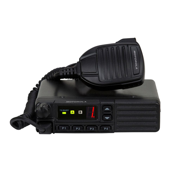
UHF Land Mobile Transceiver
VX-2000U
Service Manual
©2003 VERTEX STANDARD CO., LTD.
40 channel version
Introduction
This manual provides technical information necessary for servicing the VX-2000U UHF Land Mobile transceiver.
The VX-2000U is carefully designed to allow the knowledgeable operator to make nearly all adjustments required for
various station conditions, modes and operator preferences simply from the controls on the panels, without opening the
case of the transceiver. The VX-2000U Operating Manual describes these adjustments, plus certain internal settings.
Servicing this equipment requires expertise in handling surface mount chip components. Attempts by non-qualified
persons to service this equipment may result in permanent damage not covered by warranty.
For the major circuit boards, each side of the board is identified by the type of the majority of components installed on
that side.
In most cases one side has only chip components, and the other has either a mixture of both chip and lead components
(trimmers, coils, electrolytic capacitors, packaged ICs, etc.), or lead components only.
While we believe the technical information in this manual is correct, Vertex Standard assumes no liability for damage
that may occur as a result of typographical or other errors that may be present. Your cooperation in pointing out any
inconsistencies in the technical information would be appreciated. Vertex Standard reserves the right to make changes in
this transceiver and the alignment procedures, in the interest of technological improvement, without notification of the
owners.
Operating Manual Reprint ............................ 2
Specifications ................................................... 7
Exploded View & Miscellaneous Parts....... 8
Block Diagram ................................................. 9
Interconnection Diagram............................. 13
Circuit Description ...................................... 15
Alignment....................................................... 19
E095490A
4 channel version
Contents
Board Unit
Main Unit ............................................................... 23
Display-1 Unit ...................................................... 55
Display-2 Unit ...................................................... 59
Vr Unit ..................................................................... 63
Mic Unit .................................................................. 64
VERTEX STANDARD CO., LTD.
4-8-8 Nakameguro, Meguro-Ku, Tokyo 153-8644, Japan
VERTEX STANDARD
US Headquarters
10900 Walker Street, Cypress, CA 90630, U.S.A.
International Division
8350 N.W. 52nd Terrace, Suite 201, Miami, FL 33166, U.S.A.
YAESU EUROPE B.V.
P.O. Box 75525, 1118 ZN Schiphol, The Netherlands
YAESU UK LTD.
Unit 12, Sun Valley Business Park, Winnall Close
Winchester, Hampshire, SO23 0LB, U.K.
VERTEX STANDARD HK LTD.
Unit 5, 20/F., Seaview Centre, 139-141 Hoi Bun Road,
Kwun Tong, Kowloon, Hong Kong
(Schematics, Layouts & Parts)
1
Advertisement
Table of Contents

Related Manuals for Vertex Standard VX-2000U


Summary of Contents for Vertex Standard VX-2000U
-
Page 1: Operating Manual Reprint
This manual provides technical information necessary for servicing the VX-2000U UHF Land Mobile transceiver. The VX-2000U is carefully designed to allow the knowledgeable operator to make nearly all adjustments required for various station conditions, modes and operator preferences simply from the controls on the panels, without opening the case of the transceiver. -
Page 2: Operating Manual Reprint
Operating Manual Reprint & C ONTROLS ONNECTORS 4 channel version 40 channel version À The following items are unique to the 40-channel Microphone Jack Connect the microphone plug to this jack. radio versions: Æ CHANNEL Selector Buttons (p) and (q) Á... - Page 3 Operating Manual Reprint REAR (Heatsink) À 13.6V DC Cable Pigtail w/Connector The supplied DC power cable must be affixed to this 2-pin connector. Á Antenna Socket The 50-ohm coaxial feedline to the antenna must be con- nected here, using a “UHF” type (PL-259) plug. Â...
-
Page 4: Setting The Volume
Operating Manual Reprint PERATION Power O Scanning Turn the VOLUME/POWER knob clockwise to turn on the ra- To activate scanning on your radio, first place the microphone in dio. The active display and channel indicators will become illu- its hanger. Now press the SCAN button momentarily. The radio minated, indicating the status of the radio. -
Page 5: Ptional A Ccessories
Operating Manual Reprint ROGRAMMABLE HANNEL ELECTIONS nel, and hold in the SEL/PRI button for 2 seconds, until a beep You can program a list of channels to be scanned, and up to two channels to be monitored on a “priority” basis. Your selections sounds and the “P”... - Page 6 Operating Manual Reprint J1003 DSUB 9-Pin Data Connector Pin Assignment Ä Ã Â Á À È Ç Æ Å À SQ: Squelch Signal Output à Not Used Carrier In: Active High (5 V / 47 kΩ) Ä GND: Ground Á RX_AUD_OUT: Received Audio Output (Two choices available) Å...
-
Page 7: Specifications
Specifications General Frequency Range (version): 400 ~ 430, 450 ~ 480 or 480 ~ 512 MHz (UHF vers. A/D/F, respectively) No. of Channels & Spacing: 4 or 40 channels 25-kHz, 12.5-kHz spacing Modes of Emission: 16K0F3E ,11K0F3E Frequency Stability: ±0.00025% Antenna Requirements: 50 ohms, unbalanced (SO-239 socket) Voltage Requirements:... - Page 8 Exploded View & Miscellaneous Parts REF. VXSTD P/N Description Qty. U24208001 TAPTITE SCREW M2.6X8 (Lot. 1~3) À U20208001 BINDING HEAD SCREW M2.6X8 (Lot. 4~) Qty. VXSTD P/N Description Á U20306002 BINDING HEAD SCREW M3X6NI Q0000062 Â U23205001 TAPTITE SCREW M2.6X5 FUSE 10A Q0000008 (Lot.
-
Page 9: Block Diagram
Block Diagram VX-2000U 4ch Front Panel Block Diagram VX-2000U 40ch Front Panel Block Diagram... - Page 10 Block Diagram Note:...
- Page 11 Block Diagram VX-2000U Main Unit Block Diagram...
- Page 12 Block Diagram Note:...
-
Page 13: Interconnection Diagram
Interconnection Diagram VX-2000U 4ch Front Interconnection Diagram... - Page 14 Interconnection Diagram VX-2000U 40ch Front Interconnection Diagram...
-
Page 15: Circuit Description
Circuit Description Receive Signal Path nal within Q1029. The 2nd IF then passes through the ceramic filter CF1001 (CFWM450G) or Incoming RF from the antenna jack is delivered CF1002 (CFWM450E) to strip away unwanted to the M Unit, and passes through a low-pass mixer products, and then is applied to the limit- filter consisting of coils L1001, L1002, L1004, and er amplifier in Q1029, which removes amplitude... -
Page 16: Transmit Inhibit
Circuit Description When a carrier appears at the discriminator, Automatic Transmitter Power Control noise is removed from the output, causing pin RF output from the final amplifier is sampled 33 of Q1039 to go high, in turn causing the "B "... - Page 17 Circuit Description (2SB1201STP-FA), Q1040 (2SC4116GR), and ference between the signals derived from the D1029 (02CZ5.6Y), with temperature compen- VCO and the crystal reference oscillator. The sation provided by thermistors TH1003/TH1004 VCO is thus phase-locked to the crystal reference and capacitors associated with the 14.5 MHz ref- oscillator.
- Page 18 Circuit Description Channel Selection & Display Channel Selection & Display (4-channel version) (40-channel version) The C button on the front panel causes The U and D buttons on the front panel HANNEL microprocessor Q1039 to select the operating fre- cause microprocessor Q1039 to select the oper- quency and CTCSS frequency data from serial ating frequency and CTCSS frequency data from EEPROM Q1048 (BR93LC66AF).
-
Page 19: Alignment
Vertex representative, or the warranty policy RF Signal Generator with calibrated output to may be voided. Vertex service technicians are ex- 550 MHz perienced with the circuitry, and are fully Deviation Meter (linear detector) equipped for part replacement and alignment. - Page 20 Alignment 50 W RF Signal Dummy Load Generator Alignment Preparation & Precautions Before beginning align"ment, connect the trans- In-Line Wattmeter ceiver to the PC using the VPL-1 Connection Ca- ble, and upload the current frequency data from Deviation RF Sampling Transceiver meter Coupler...
- Page 21 Alignment PLL VCV (Varactor Control Voltage) Transmitter Output Power Performance Check Preset trimmer potentiometer VR1002 (MAIN Unit) fully clockwise. Connect the DC voltmeter between test point Select (Band center) channel 2. Key the trans- TP1033 on the MAIN Unit and chassis ground. mitter, and confirm that at least 30 Watts of Set the transceiver to channel 3, and confirm power output is measured.
- Page 22 Alignment Receiver Squelch Threshold Reduce the AF generator’s output to zero. Key the transmitter, and adjust VR1004 (MAIN Set the transceiver to channel 2. Set the RF sig- Unit) for ±800 Hz deviation on the CTCSS tone nal generator to the same frequency (415.000 (within 100 Hz).
- Page 23 MAIN Unit (Lot. 1~) 7.8 (7.8) Circuit Diagram 3.3 (4.0) 2.7 (4.0) 13.6 (13.5) 0 (3.4) 0 (8.0) 7.3 (7.3) 7.4 (7.4) 3.5 (3.5) 13.3 (11.8) 0 (4.7) 0 (5.9) 0 (7.3) 0 (0.8) 0 (8.6) (1.1) 0 (1.1) 2.8 (8.2) 90 mV 0 (8.6) 0 (0.1)
- Page 24 MAIN Unit (Lot. 1~) Note:...
- Page 25 MAIN Unit (Lot. 1~) Parts Layout MB89P677ARFM (Lot. 1~) MX165BDW MB89677ARPFM (Lot. 2~) (Q1009) (Q1039) SC370651FR2 BA4116FV (Q1049) TA31136FN (Lot. 2~) (Q1029) NJM2902V NJM2904V (Q1007, 1016) (Q1017) TDA2003H 2SB1143S (Q1003) (Q1014) Side A HA17805P 2SB1201STP (Q1010) (Q1002) RH5VA45AA (D5) 2SC4116GR (LG) (Q1036) (Q1015, 1042) 2SC4215Y (QY)
- Page 26 MAIN Unit (Lot. 1~) Side B M57729H BR93LC66RF IMH6 (H6) DTB123EK (F12) DTC124EU (25) 2SC4116GR (LG) HZM7C (24) MA143 (MC) 1SS321 (F9) (Q1011) (Q1048) (Q1004, 1025, 1052) (Q1006) (Q1020, 1033, 1051) (Q1040, 1045, 1046) (D1024) (D1037) (D1006) 2SC5107O (MFO) MA142WK (MU) (Q1038, 1041) (D1019) DAN235K (M)
- Page 27 MAIN Unit (Lot. 4~) Circuit Diagram...
- Page 28 MAIN Unit (Lot. 4~) Note:...
- Page 29 MAIN Unit (Lot. 4~) Parts Layout MB89P677ARFM (Lot. 1~) MX165BDW MB89677ARPFM (Lot. 2~) MX165CDW (Lot. 5~) (Q1039) (Q1009) SC370651FR2 BA4116FV (Q1049) TA31136FN (Lot. 2~) (Q1029) NJM2902V NJM2904V (Q1007, 1016) (Q1017) TDA2003H 2SB1143S (Q1003) (Q1014) Side A HA17805P 2SB1201STP (Q1010) (Q1002) RH5VA45AA (D5) 2SC4116GR (LG) (Q1036)
- Page 30 MAIN Unit (Lot. 4~) Side B M57729H M57729L (Ver. A : Lot. 4~) BR93LC66RF IMH6 (H6) DTB123EK (F12) DTC124EU (25) 2SC4116GR (LG) HZM7C (24) MA143 (MC) 1SS321 (F9) M57729SH-01 (Ver. F : Lot. 5~) (Q1048) (Q1004, 1025, 1052) (Q1006) (Q1020, 1033, 1051) (Q1040, 1045, 1046) (D1024) (D1037)
- Page 31 MAIN Unit (Lot. 7~) Circuit Diagram...
- Page 32 MAIN Unit (Lot. 7~) Note:...
- Page 33 MAIN Unit (Lot. 7~) Parts Layout MB89P677ARFM (Lot. 1~) MX165BDW MB89677ARPFM (Lot. 2~) MX165CDW (Lot. 5~) (Q1039) (Q1009) SC370651FR2 BA4116FV (Q1049) TA31136FN (Lot. 2~) (Q1029) NJM2902V NJM2904V (Q1007, 1016) (Q1017) TDA2003H 2SB1143S (Q1003) (Q1014) Side A HA17805P 2SB1201STP (Q1010) (Q1002) 2SC4116GR (LG) RH5VA45AA (D5) (Q1015, 1042)
- Page 34 MAIN Unit (Lot. 7~) Side B M57729H M57729L (Ver. A : Lot. 4~) BR93LC66RF IMH6 (H6) DTB123EK (F12) DTC124EU (25) 2SC4116GR (LG) HZM7C (24) MA143 (MC) 1SS321 (F9) M57729SH-01 (Ver. F : Lot. 5~) (Q1048) (Q1004, 1025, 1052) (Q1006) (Q1020, 1033, 1051) (Q1040, 1045, 1046) (D1024) (D1037)
- Page 35 MAIN Unit (Lot. 10~) Circuit Diagram...
- Page 36 MAIN Unit (Lot. 10~) Note:...
- Page 37 MAIN Unit (Lot. 10~) Parts Layout MB89P677ARFM (Lot. 1~) MX165BDW MB89677ARPFM (Lot. 2~) MX165CDW (Lot. 5~) (Q1039) (Q1009) SC370651FR2 BA4116FV MC145192FR2 (Lot. 19~) TA31136FN (Lot. 2~) MC145193FR2 (Lot. 23~) (Q1029) (Q1049) NJM2902V NJM2904V (Q1007, 1016) (Q1017) TDA2003H 2SB1143S (Q1003) (Q1014) Side A HA17805P (Lot.
- Page 38 MAIN Unit (Lot. 10~) Side B M57729H M57729L (Ver. A : Lot. 4~) BR93LC66RF IMH6 (H6) DTB123EK (F12) DTC124EU (25) 2SC4116GR (LG) HZM7C (24) MA143 (MC) 1SS321 (F9) M57729SH-01 (Ver. F : Lot. 5~) BR93L66RF (Lot. 62~) (Q1004, 1025, 1052) (Q1006) (Q1020, 1033, 1051) (Q1040, 1045, 1046)
-
Page 39: Main Unit
MAIN Unit Parts List REF. DESCRIPTION VALUE TOL. MFR’S DESIG VXSTD P/N VERS. LOT. SIDE. LAY ADR. *** MAIN UNIT *** PCB with Components CS1573001 TYPE D PCB with Components CS1573002 TYPE A PCB with Components CS1573003 TYPE F Printed Circuit Board FR002190B Printed Circuit Board FR002190C... - Page 40 MAIN Unit REF. DESCRIPTION VALUE TOL. MFR’S DESIG VXSTD P/N VERS. LOT. SIDE. LAY ADR. C 1041 CHIP CAP. GRM39CK010C50PT K22174202 C 1041 CHIP CAP. GRM39CK010C50PT K22174202 VERSION D 4- C 1041 CHIP CAP. GRM39CH050C50PT K22174206 VERSION F 5- C 1042 CHIP CAP. 0.001uF GRM39B102M50PT K22174809...
- Page 41 MAIN Unit REF. DESCRIPTION VALUE TOL. MFR’S DESIG VXSTD P/N VERS. LOT. SIDE. LAY ADR. C 1073 CHIP CAP. GRM39CH050C50PT K22174206 C 1073 CHIP CAP. GRM39CH070D50PT K22174208 VERSION A 4- C 1073 CHIP CAP. GRM39CH050C50PT K22174206 VERSION D 4- C 1073 CHIP CAP. GRM39CH080D50PT K22174209 VERSION F 5- C 1074 CHIP CAP.
- Page 42 MAIN Unit REF. DESCRIPTION VALUE TOL. MFR’S DESIG VXSTD P/N VERS. LOT. SIDE. LAY ADR. C 1106 CHIP CAP. GRM39CH040C50PT K22174205 VERSION F 5- C 1107 CHIP CAP. 18pF GRM39CH180J50PT K22174217 C 1107 CHIP CAP. 15pF GRM39CH150J50PT K22174215 7-36 A C 1107 CHIP CAP.
- Page 43 MAIN Unit REF. DESCRIPTION VALUE TOL. MFR’S DESIG VXSTD P/N VERS. LOT. SIDE. LAY ADR. C 1147 CHIP CAP. 0.001uF GRM39B102K50PT K22174821 C 1149 CHIP CAP. 39pF GRM39CH390J50PT K22174225 C 1150 CHIP CAP. 0.33uF GRM40B334K16PT K22120807 C 1151 CHIP CAP. 0.001uF GRM39B102K50PT K22174821...
- Page 44 MAIN Unit REF. DESCRIPTION VALUE TOL. MFR’S DESIG VXSTD P/N VERS. LOT. SIDE. LAY ADR. C 1202 CHIP CAP. 100pF GRM39CH101J50PT K22174235 C 1203 CHIP CAP. 33pF GRM39CH330J50PT K22174223 C 1204 CHIP CAP. 0.001uF GRM39B102K50PT K22174821 C 1205 CHIP CAP. GRM39CH070D50PT K22174208 C 1206 CHIP CAP.
- Page 45 MAIN Unit REF. DESCRIPTION VALUE TOL. MFR’S DESIG VXSTD P/N VERS. LOT. SIDE. LAY ADR. C 1259 CHIP CAP. 220pF GRM39CH221J50PT K22174243 C 1260 TANTALUM CAP. 10uF DN1C100M1S K70127106 C 1260 CHIP TA.CAP. 10uF TEMSVA1A106M-8R K78100028 C 1261 CHIP CAP. GRM39F105Z10PT K22105001 C 1262 CHIP CAP.
- Page 46 MAIN Unit REF. DESCRIPTION VALUE TOL. MFR’S DESIG VXSTD P/N VERS. LOT. SIDE. LAY ADR. D 1035 DIODE 1SV230 TPH3 G2070126 D 1036 DIODE DAP202U T106 G2070160 D 1037 DIODE MA143-(TX) G2070536 D 1038 DIODE 1SV276(TPH3) G2070420 D 1039 DIODE 1SV276(TPH3) G2070420 D 1040 DIODE...
- Page 47 MAIN Unit REF. DESCRIPTION VALUE TOL. MFR’S DESIG VXSTD P/N VERS. LOT. SIDE. LAY ADR. L 1018 COIL E2 0.26-0.9-3T-R L0022367 VERSION A 5- L 1018 COIL E2 0.26-0.9-3T-R L0022367 VERSION D 5- L 1018 COIL E2 0.3-0.9-3T-R L0022389 VERSION F 5- L 1019 M.RFC 0.0498uH 36CS 656LZ-09K=P3...
- Page 48 R 1003 CHIP RES. RMC1 4R7JTE J24305479 R 1004 CHIP RES. 1/10W 5% RMC1/10T 1R0J J24205010 R 1006 CHIP RES. 1/16W 5% RMC1/16 102JATP J24185102 1-36 B R 1006 CHIP RES. 1/16W 5% RMC1/16 102JATP J24185102 DST:THA * Please contact VERTEX STANDARD.
- Page 49 MAIN Unit REF. DESCRIPTION VALUE TOL. MFR’S DESIG VXSTD P/N VERS. LOT. SIDE. LAY ADR. R 1006 CHIP RES. 1/16W 5% RMC1/16 102JATP J24185102 EXPORT R 1006 CHIP RES. 1/16W 5% RMC1/16 102JATP J24185102 STANDARD 37- R 1006 CHIP RES. 1/16W 5% RMC1/16 102JATP J24185102 THAILAND...
- Page 50 MAIN Unit REF. DESCRIPTION VALUE TOL. MFR’S DESIG VXSTD P/N VERS. LOT. SIDE. LAY ADR. R 1059 CHIP RES. 180k 1/16W 5% RMC1/16 184JATP J24185184 R 1061 CHIP RES. 100k 1/16W 5% RMC1/16 104JATP J24185104 R 1062 CHIP RES. 820k 1/16W 5% RMC1/16 824JATP J24185824...
- Page 51 MAIN Unit REF. DESCRIPTION VALUE TOL. MFR’S DESIG VXSTD P/N VERS. LOT. SIDE. LAY ADR. R 1106 CHIP RES. 1/10W 5% RMC1/10T 471J J24205471 R 1107 CHIP RES. 1/16W 5% RMC1/16 223JATP J24185223 R 1108 CHIP RES. 1/16W 5% RMC1/16 471JATP J24185471 R 1109 CHIP RES.
- Page 52 MAIN Unit REF. DESCRIPTION VALUE TOL. MFR’S DESIG VXSTD P/N VERS. LOT. SIDE. LAY ADR. R 1154 CHIP RES. 1/16W 5% RMC1/16 331JATP J24185331 R 1156 CHIP RES. 2.2k 1/16W 5% RMC1/16 222JATP J24185222 R 1157 CHIP RES. 1/16W 5% RMC1/16 103JATP J24185103 R 1158 CHIP RES.
- Page 53 MAIN Unit DESCRIPTION VALUE TOL. MFR’S DESIG VXSTD P/N VERS. LOT. SIDE. LAY ADR. R 1207 CHIP RES. 1/16W 5% RMC1/16 103JATP J24185103 R 1208 CHIP RES. 1/16W 5% RMC1/16 103JATP J24185103 R 1209 CHIP RES. 1/16W 5% RMC1/16 103JATP J24185103 R 1210 CHIP RES.
- Page 54 MAIN Unit REF. DESCRIPTION VALUE TOL. MFR’S DESIG VXSTD P/N VERS. LOT. SIDE. LAY ADR. R 1254 CHIP RES. 1/16W 5% RMC1/16 102JATP J24185102 R 1255 CHIP RES. 1/16W 5% RMC1/16 221JATP J24185221 R 1255 CHIP RES. 1/16W 5% RMC1/16 221JATP J24185221 VERSION D 4-9 R 1256 CHIP RES.
-
Page 55: Display-1 Unit
Display-1 Unit Circuit Diagram... - Page 56 Display-1 Unit Parts Layout Side A Side B BU4094BCFV XN1213 (9L) DTC124EK (25) (Q2002) (Q2001, 2003, 2004) (Q2005)
-
Page 57: Parts List
Display-1 Unit Parts List REF. DESCRIPTION VALUE TOL. MFR’S DESIG VXSTD P/N VERS. LOT. SIDE. LAY ADR. *** DISPLAY-1 UNIT *** PCB with Components CB0382001 Printed Circuit Board FR001580B D 2001 LED HLMP-1540 G2090696 D 2002 LED HLMP-1540 G2090696 D 2003 LED HLMP-1540 G2090696 D 2004 LED... - Page 58 Display-1 Unit Note:...
-
Page 59: Display-2 Unit
Display-2 Unit Circuit Diagram... - Page 60 Display-2 Unit Parts Layout Side A Side B DN8657S DTC124EK (25) (Q3001) (Q3003) Dig.1 Dig.2 D.P2 D.P1 A1 B1 C1 D1 E1 F1 G1 A2 B2 C2 D2 E2 F2 G2 16 15 1 18 17 11 10 XN1213 (9L) (Q3002) DS3001 7-Segment LCD Display...
- Page 61 Display-2 Unit Parts List REF. DESCRIPTION VALUE TOL. MFR’S DESIG VXSTD P/N VERS. LOT. SIDE. LAY ADR. *** DISPLAY-2 UNIT *** PCB with Components CB0383001 Printed Circuit Board FR001590B D 3002 DIODE 1SS355 TE-17 G2070470 D 3003 LED TLY211 G2090637 D 3004 DIODE 1SS355 TE-17 G2070470...
- Page 62 Display-2 Unit Note:...
- Page 63 VR Unit Circuit Diagram Parts Layout Side A Side B Parts List REF. DESCRIPTION VALUE TOL. MFR’S DESIG VXSTD P/N VERS. LOT. SIDE. LAY ADR. *** VR UNIT *** PCB with Components CB0384001 Printed Circuit Board FR001600B VR4001 POT. RK0971111 10KB/SW J60800228...
-
Page 64: Mic Unit
MIC Unit Circuit Diagram Parts Layout Side A Side B Parts List REF. DESCRIPTION VALUE TOL. MFR’S DESIG VXSTD P/N VERS. LOT. SIDE. LAY ADR. *** MIC UNIT *** PCB with Components CB0385001 Printed Circuit Board FR001600B D 5001 DIODE 1SS355 TE-17 G2070470 J 5001 CONNECTOR... - Page 65 No portion of this manual © Copyright 2003 may be reproduced VERTEX STANDARD CO., LTD. without the ermission of All rights reserved VERTEX STANDARD CO., LTD.