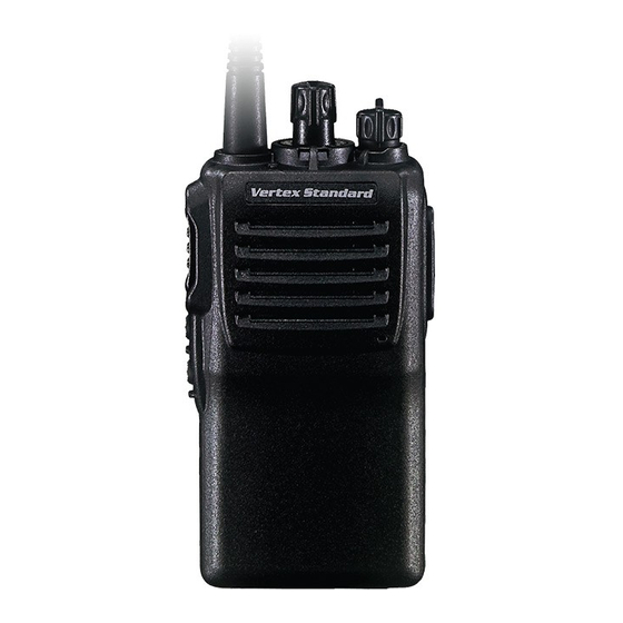
Vertex Standard VX-230 Service Manual
Vhf fm transceiver
Hide thumbs
Also See for VX-230:
- Service manual (38 pages) ,
- Specification sheet (2 pages) ,
- Operating manual (2 pages)
Advertisement
Quick Links
VHF FM Transceiver
VX-230
Service Manual
© 2008 VERTEX STANDARD CO., LTD.
Introduction
This manual provides technical information necessary for servicing the VX-230 FM Transceiver.
Servicing this equipment requires expertise in handling surface-mount chip components. Attempts by non-qualified persons to ser-
vice this equipment may result in permanent damage not covered by the warranty, and may be illegal in some countries.
Two PCB layout diagrams are provided for each double-sided circuit board in the transceiver. Each side of is referred to by the type
of the majority of components installed on that side ("leaded" or "chip-only"). In most cases one side has only chip components, and
the other has either a mixture of both chip and leaded components (trimmers, coils, electrolytic capacitors, ICs, etc.), or leaded
components only.
While we believe the technical information in this manual to be correct, VERTEX STANDARD assumes no liability for damage that
may occur as a result of typographical or other errors that may be present. Your cooperation in pointing out any inconsistencies in the
technical information would be appreciated.
This transceiver was assembled using Pb (lead) free solder, based on the RoHS specification.
Only lead-free solder (Alloy Composition: Sn-3.0Ag-0.5Cu) should be used for repairs performed on this apparatus. The
solder stated above utilizes the alloy composition required for compliance with the lead-free specification, and any solder with
the above alloy composition may be used.
Specifications........................................................... 2
Exploded View & Miscellaneous Parts ................. 3
Block Diagram ........................................................ 5
Circuit Description ................................................ 7
EC085N90A
Important Note
Contents
Alignment ............................................................... 9
MAIN Unit Circuit Diagram .............................. 17
MAIN Unit Parts Layout .................................... 19
MAIN Unit Parts List .......................................... 21
VERTEX STANDARD CO., LTD.
4-8-8 Nakameguro, Meguro-Ku, Tokyo 153-8644, Japan
VERTEX STANDARD
US Headquarters
10900 Walker Street, Cypress, CA 90630, U.S.A.
YAESU EUROPE B.V.
P.O. Box 75525, 1118 ZN Schiphol, The Netherlands
YAESU UK LTD.
Unit 12, Sun Valley Business Park, Winnall Close
Winchester, Hampshire, SO23 0LB, U.K.
VERTEX STANDARD HK LTD.
Unit 5, 20/F., Seaview Centre, 139-141 Hoi Bun Road,
Kwun Tong, Kowloon, Hong Kong
VERTEX STANDARD ( AUSTRALIA ) PTY., LTD.
Normanby Business Park, Unit 14/45 Normanby Road
Notting Hill 3168, Victoria, Australia
1
Advertisement

Related Manuals for Vertex Standard VX-230


Summary of Contents for Vertex Standard VX-230
-
Page 1: Table Of Contents
While we believe the technical information in this manual to be correct, VERTEX STANDARD assumes no liability for damage that may occur as a result of typographical or other errors that may be present. Your cooperation in pointing out any inconsistencies in the technical information would be appreciated. -
Page 2: Specifications
Specifications General Frequency Range: 134 -174 MHz Number of Channels: Power Supply Voltage: 7.4 V DC ±10 % Channel Spacing: 12.5/20/25 kHz Battery Life (5-5-90 duty): 9.0 hrs (7.3 hrs w/o saver) w/FNB-V103LI (1150 mAh) 16.5 hrs (13.5 hrs w/o saver) w/FNB-V104LI (2000 mAh) Operating Temperature Range: –22 °F to +140 °F (–30 °C to +60 °C) Frequency Stability: ±2.5 ppm... -
Page 3: Exploded View & Miscellaneous Parts
Exploded View & Miscellaneous Parts RA1096000 COIL SPRING RA0173500 CAP (MIC/SP) CP9380001 FRONT CASE ASSY RA1058900 O RING RA103980A RA090600C RELEASE KNOB(BATT) KNOB(VOL) RA0905200 RA091760B LATCH PLATE KNOB ASSY(CH) RA1041900 RA090490B FRAME(PTT) COVER(PTT) RA1041800 RA1041700 RUBBER(SIDE) RUBBER(PTT) RA0187600 RA1042100 SHEET LOCK PLATE T9318321 RA0557900... - Page 4 Note...
-
Page 5: Block Diagram
Block Diagram... - Page 6 Block Diagram Note...
-
Page 7: Circuit Description
Circuit Description 1. Circuit Configuration by Frequency 2-5. Squelch Circuit The receiver is a Double-conversion Super-heterodyne with a There are 16 levels of squelch setting from 0 to 15. The level 0 first intermediate frequency (IF) of 67.65MHz and a second IF means open the squelch. - Page 8 Circuit Description 3-2. Drive and Final amplifier 3-4-2. VCO Tuning Voltage The modulated signal from the VCO Q1032 (2SC4227) is buff- Tuning voltage of VCO is expanding the lock range of VCO by ered by Q1027 (2SC5005). Then the signal is buffered by controlling the cathode of varactor diode at the voltage and the Q1018 (2SC5227) for the final amplifier driver Q1015 control voltage from PLL IC.
-
Page 9: Alignment
Alignment Introduction Required Test Equipment The VX-230 series has been aligned at the factory for the spec- Radio Tester with calibrated output level at 200 MHz ified performance across the entire frequency range specified. In-line Wattmeter with 5% accuracy at 200 MHz... - Page 10 Alignment Test Setup Basic Alignment Mode Setup the test equipment as shown for transceiver alignment, In the Basic Alignment mode, the aligned data written in the then apply 7.5 V DC power to the transceiver. radio will be able to re-align its alignment data. In this mode, there are many items to align with five points (F1, F2, F3, F4, 50-ohm F5) except "Frequency", "Mic Sense", "SQL/RSSI", and "Bat-...
- Page 11 Alignment 1. PLL R EFERENCE REQUENCY REQUENCY This parameter is to align the reference frequency for PLL. 1. Press the “Frequency” button to start the alignment then the radio will transmit on the center frequency. It will appear the Frequency Alignment window. 2..Click the “PTT”...
- Page 12 Alignment ( SQL ) 3. S QUELCH This parameter is to align the SQL (Squelch) Sensitivity. There are several alignments as follows in the Squelch Sensitivity. Threshold SQL Level The Alignment for the Noise SQL Threshold level at Wide (5k/ 4k).
- Page 13 Alignment 5. M ENSE This parameter is to align the Microphone Sense (Gain) and it needs the appropriate JIG (Tuning Interface BOX). Connect the JIG and Test Equipment to the radio before the alignment is going to start. It must be done alignment of the "Max Deviation" before this alignment is going to start.
- Page 14 Alignment 7. M <W > / <N > ODULATION ALANCE ARROW LIGNMENT IS DIFFICULT This parameter is to align the Modulation Deviation (Wide/Narrow) and it needs the appropriate JIG (Tuning Interface BOX). Connect the JIG and Test Equipment to the radio before the alignment is going to start.It must be done alignment of the "Max Deviation"...
- Page 15 Alignment 9. DCS D <W > / <N > EVIATION ARROW This parameter is to align DCS Deviation of the selected channel. 1. Input the desired DCS Code on the DCS Code Box. Default: 523 Input Range: 000 to 777 2.
- Page 16 Note...
-
Page 17: Main Unit Circuit Diagram
MAIN Unit Circuit Diagram RX: 2.6 V +7 dBµ TX: 0 V RX: 0 V –4 dBµ TX: 0.9 V RX: 2.1 V TX: 0 V +3 dBµ –8 dBµ –11 dBµ RX: 0.7 V TX: 0 V 5.0 V RX: 0 V 4.2 V TX: 3.9 V... - Page 18 MAIN Unit Note...
-
Page 19: Main Unit Parts Layout
MAIN Unit Parts Layout (Side A) TC74VHC4066AFT (Q1001) NJM12902V (Q1046, 1049, 1050) 2SC4081 (B) (Q1037) 2SC4617 (BR) (Q1002, 1007) TAR5S50U (5V0) (Q1003) TAR5S35U (3V5) (Q1020) NJM2070M-TE1 (Q1005) MTM231230L (BL) (Q1006, 1008, 1011) 2SK3541 (Q1056) DTC144EE (26) (Q1009, 1014, 1045) DA221 (K) NJM12904R DTA144EE (16) UPD78F1142GB(S)-GAH-AX... - Page 20 MAIN Unit Parts Layout (Side B) 2SC5006 (24) (Q1013) 2SC4617 (BR) (Q1016, 1034) 2SC5227 (Q1018) 2SC5005 (73) (Q1027) 2SC4227 (R32) (Q1032) 2SC4215Y (QY) (Q1033) RQA0004PXDQS (PX) (Q1015) 3SK293 (HF) (Q1024) 2SK508 (K52) (Q 1030) DA221 (K) DAN222 (N) DTC144EE (26) NJM2591V DTC114TE (04) (D1019, 1035)
-
Page 21: Main Unit Parts List
MAIN Unit Parts List REF. DESCRIPTION VALUE TOL. MFR’S DESIG VXSTD P/N VERS. LOT. SIDE LAY ADR PCB with Components CS2010401 DST:VTX CS2010402 DST:EXP Printed Circuit Board AC085N000 FR018730D C 1001 CHIP CAP. 47pF GRM1552C1H470JZ01D K22178228 C 1002 CHIP CAP. 0.001uF GRM155B11H102KA01D K22178809... - Page 22 MAIN Unit Parts List REF. DESCRIPTION VALUE TOL. MFR’S DESIG VXSTD P/N VERS. LOT. SIDE LAY ADR C 1086 CHIP CAP. 0.001uF GRM155B11H102KA01D K22178809 C 1087 CHIP CAP. 220pF GRM1552C1H221JA01D K22179713 C 1089 CHIP CAP. 0.1uF GRM155B11A104KA01D K22108802 C 1090 CHIP CAP.
- Page 23 MAIN Unit Parts List REF. DESCRIPTION VALUE TOL. MFR’S DESIG VXSTD P/N VERS. LOT. SIDE LAY ADR C 1179 CHIP CAP. 6.3V GRM188B10J105KA01D K22084801 C 1180 CHIP CAP. GRM1552C1H6R0DZ01D K22178208 C 1182 CHIP CAP. 150pF GRM1552C1H151JA01D K22178240 C 1183 CHIP CAP. 0.1uF GRM155B11A104KA01D K22108802...
- Page 24 MAIN Unit Parts List REF. DESCRIPTION VALUE TOL. MFR’S DESIG VXSTD P/N VERS. LOT. SIDE LAY ADR C 1276 CHIP CAP. 0.0033uF GRM155B11H332KA01D K22178815 C 1277 CHIP CAP. 0.1uF GRM155B11A104KA01D K22108802 C 1278 CHIP CAP. 0.1uF GRM155B11A104KA01D K22108802 C 1279 CHIP CAP.
- Page 25 MAIN Unit Parts List REF. DESCRIPTION VALUE TOL. MFR’S DESIG VXSTD P/N VERS. LOT. SIDE LAY ADR D 1008 DIODE 1SV325(TPH3.F) G2070848 D 1009 DIODE 1SS400 TE61 G2070634 D 1010 DIODE EDZ TE-61 3.9B G2071004 D 1011 DIODE 1SS400 TE61 G2070634 D 1012 DIODE...
- Page 26 R 1037 CHIP RES. 270k 1/16W 0.5% MCR01MZPD2703 J24189329 R 1038 CHIP RES. 1/16W 5% RMC1/16S 223JTH J24189041 R 1040 CHIP RES. 1/16W 5% RMC1/16S 223JTH J24189041 R 1041 CHIP RES. 100k 1/16W 5% RMC1/16S 104JTH J24189049 Please contact VERTEX STANDARD.
- Page 27 MAIN Unit Parts List REF. DESCRIPTION VALUE TOL. MFR’S DESIG VXSTD P/N VERS. LOT. SIDE LAY ADR R 1042 CHIP RES. 1/16W 5% RMC1/16S 101JTH J24189013 R 1043 CHIP RES. 4.7k 1/16W 5% RMC1/16S 472JTH J24189033 R 1044 CHIP RES. 1/16W 5% RMC1/16S 331JTH J24189019...
- Page 28 MAIN Unit Parts List REF. DESCRIPTION VALUE TOL. MFR’S DESIG VXSTD P/N VERS. LOT. SIDE LAY ADR R 1137 CHIP RES. 1/16W 5% RMC1/16S 180JTH J24189004 R 1138 CHIP RES. 100k 1/16W 5% RMC1/16S 104JTH J24189049 R 1140 CHIP RES. 100k 1/16W 5% RMC1/16S 104JTH...
- Page 29 MAIN Unit Parts List REF. DESCRIPTION VALUE TOL. MFR’S DESIG VXSTD P/N VERS. LOT. SIDE LAY ADR R 1231 CHIP RES. 100k 1/16W 0.5% MCR01MZPD1003 J24189386 R 1233 CHIP RES. 1/16W 0.5% MCR01MZPD5600 J24189359 R 1234 CHIP RES. 100k 1/16W 0.5% MCR01MZPD1003 J24189386 R 1235...
- Page 30 MAIN Unit Note:...
- Page 32 Copyright 2008 VERTEX STANDARD CO., LTD. All rights reserved No portion of this manual may be reproduced without the permission of VERTEX STANDARD CO., LTD.