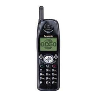
Panasonic EB-GD30 Service Manual
Portable handheld
Hide thumbs
Also See for EB-GD30:
- Operating instructions manual (60 pages) ,
- Technical manual (45 pages)
Table of Contents
Advertisement
Quick Links
Download this manual
See also:
Technical Manual
Service Manual
This service information is designed for experienced repair technicians only and is not designed for use by the general public. It does not contain warnings or
cautions to advise non-technical individuals of potential dangers in attempting to service a product.
Products powered by electricity should be serviced or repaired only by experienced professional technicians. Any attempt to service or repair the product or
products dealt with in this service manual by anyone else could result in serious injury or death.
Issue 1
Revision 0
© by
]CC[Toko
Frequency range
Tx/Rx frequency separation
RF channel bandwidth
Number of RF channels
Speech coding
Operating temperature
Type
RF Output Power
Modulation
Connection
Voice digitizing
Transmission speed
Diversity
Signal Reception
Intermediate Frequencies
Antenna Terminal Impedance
Antenna VSWR
Dimensions
Volume
Weight
Display
Illumination
Keypad
SIM
External DC Supply Voltage
Battery
Standby Battery Life
DRX 9
Conversation Battery Life
PL 7, DTX 50%
WARNING
Order Number: MCUK991001C8
Handheld Portable
Specification
900 MHz
Tx: 890 - 915 MHz
Tx: 1710 - 1785 MHz
Rx: 935 - 960 MHz
Rx: 1805 - 1880 MHz
45 MHz
200 kHz
124
Full rate/Half rate/Enhanced
Full rate/Half rate
Full rate
-10°C to +55°C
Class 4 Handheld
Class 1 Handheld
2 W maximum
1 W maximum
GMSK (BT = 0.3)
8 ch/TDMA
13 kbps RPE-LTP / 13 kps ACLEP / 5.6 kps CELP / VSLEP
270.3 kbps
Frequency hopping
Double superheterodyne
282 MHz and 45 MHz
50 Ω
<2.1 : 1
Height: 135 mm
Width:
45 mm
Depth:
20.5 mm (30 mm with EB-BLD30 Battery)
123 cc (150 cc with EB-BLD30 Battery)
GD30: 130 g (170 g with EB-BLD30 Battery)
GD50: 115 g (170 g with EB-BLD30 Battery)
Graphical chip on glass liquid crystal, Alphanumeric,
16 x 3 characters, 5 icons and 6 x 1 characters
4 LEDs for the LCD (Green)
8 LEDs for the keypad (Green)
1 LED Incoming call (Green)
1 Charging LED (Red)
17 keys, Navigation key
Plug-in type only
3.6 V
EB-BSD30: 3.6 V nominal, 670mAh, Ni-MH
EB-BSD50: 3.6 V nominal, 670mAh, Li-Ion
EB-BLD30: 3.6V nominal, 1340mAh, Ni-MH
EB-BSD30/EB-BSD50: 95 hrs maximum
EB-BLD30: 190 hrs maximum
EB-BSD30/EB-BSD50: 180 minutes
EB-BLD30: 360 minutes
Battery life figures are dependent on network conditions.
EB-GD30
EB-GD50
1800 MHz
95 MHz
374
Advertisement
Table of Contents

Related Manuals for Panasonic EB-GD30


Summary of Contents for Panasonic EB-GD30
- Page 1 Order Number: MCUK991001C8 Service Manual © by ]CC[Toko Handheld Portable EB-GD30 EB-GD50 Specification 900 MHz 1800 MHz Frequency range Tx: 890 - 915 MHz Tx: 1710 - 1785 MHz Rx: 935 - 960 MHz Rx: 1805 - 1880 MHz Tx/Rx frequency separation...
- Page 2 This Service Manual is copyright and issued on the strict understanding that it is not to be reproduced, copied, or disclosed to any third party, either in whole or part, without the prior written consent of Matsushita Communication Industrial UK Ltd. Every care has been taken to ensure that the contents of this manual give an accurate representation of the equipment.
-
Page 3: Warnings And Cautions
WARNINGS AND CAUTIONS WARNING The equipment described in this manual contains polarized capacitors utilising liquid electrolyte. These devices are entirely safe provided that neither a short-circuit nor a reverse polarity connection is made across the capacitor terminals. FAILURE TO OBSERVE THIS WARNING COULD RESULT IN DAMAGE TO THE EQUIPMENT OR, AT WORST, POSSIBLE INJURY TO PERSONNEL RESULTING FROM ELECTRIC SHOCK OR THE AFFECTED CAPACITOR EXPLODING. - Page 4 This page is left intentionally blank. Issue 1 – iv – MCUK991001C8 Revision 0 Service Manual...
-
Page 5: Table Of Contents
CONTENTS 1 INTRODUCTION Purpose of this Manual ......1 Structure of the Manual ......1 Servicing Responsibilities . - Page 6 This page is left intentionally blank. Issue 1 Section MCUK991001C8 Revision 0 – vi – Service Manual...
-
Page 7: Introduction
INTRODUCTION 1.1 Purpose of this Manual This Service Manual contains the information and procedures required for installing, operating and servicing the Panasonic GSM Personal Cellular Mobile Telephone system operating on the GSM Digital Cellular Network. 1.2 Structure of the Manual... - Page 8 INTRODUCTION This page is left intentionally blank. Issue 1 Section 1 MCUK991001C8 Revision 0 – 2 – Service Manual...
-
Page 9: General Description
This section provides a general description and kit composition details for the GSM Handportable Telephone system and optional kits. Panasonic Model Numbers GD30 and GD50 are high performance, small, light, business GSM telephones. The following features are included as standard: Triple Rate which includes Full Rate, Half Rate and Enhanced Full Rate (EFR) speech, codec. - Page 10 GENERAL DESCRIPTION This page is left intentionally blank. Issue 1 Section 2 MCUK991001C8 Revision 0 – 4 – Service Manual...
-
Page 11: Operating Instructions
OPERATING INSTRUCTIONS OPERATING INSTRUCTIONS 3.1 General This section provides a brief guide to the operation and facilities available on the GD30 and GD50 mobile telephones. Refer to the Operating Instructions supplied with the telephones for full operational information. 3.2 LCD Display The handportable unit has a graphical chip on glass liquid crystal display in conjunction with the following icons: Menu Number Option Area... -
Page 12: Location Of Controls
OPERATING INSTRUCTIONS 3.3 Location of Controls Incoming/Charge indicator: Green – incoming call. Red – charging battery pack. External connector: Used to connect to external accessories or charging equipment. Figure 3.2: Location of controls for GD30/GD50 Navigation Key. Scrolls through options or features menu and increases or decreases volume. Select Key. -
Page 13: Concept Of Operation
OPERATING INSTRUCTIONS 3.4 Concept of Operation There is a close relationship between the Select Key, Navigation Key and display. Figure 3.3: Concept of Operation Pressing up and down ( ) will move the pointer up and down and scroll through more information in the main area of the display. -
Page 14: Hot Key Dial Source List
OPERATING INSTRUCTIONS 3.7 Hot Key Dial Source List The source for Hot Key Dial Numbers is normally ‘Phonebook’ or ‘Service Dial Numbers’. For some OEMs it may be a requirement to store these numbers in the EEPROM. When the source is the EEPROM and the telephone software is updated, the source numbers may be lost. -
Page 15: Public Man Machine Interface (Mmi)
OPERATING INSTRUCTIONS 3.9 Public Man Machine Interface (MMI) It is possible to operate all GSM telephones in the same way using the Public MMI. The following operations will work with all GSM telephones. However, this information is restricted to those operations that are supported by GD30 and GD50 telephones. The * and # in the following procedures should be replaced by , respectively. -
Page 16: Calling Line Identification
OPERATING INSTRUCTIONS 3.9.6 Calling Line Identification Calling Line Identification Feature Service Code Calling Line Identification Presentation (CLIP) Calling Line Identification Restriction (CLIR) Connected Line Presentation (CLOP) Connected Line Restriction (CLOR) Enable * <SERVICE CODE> * # <SND> Disable # <SERVICE CODE> * # <SND> Temporary suppress identification # 3 1 # <TELEPHONE NUMBER>... -
Page 17: Call Bar
OPERATING INSTRUCTIONS Status * # <SERVICE CODE> * <TELECOMMUNICATION SERVICE> * # <SND> Clear all Call Diverts # # 0 0 2 # 3.9.9 Call Bar Call Bar Type Service Code All outgoing calls Outgoing international calls Outgoing international calls except those to the PLMN country All incoming calls Incoming international calls when roaming * <PASSWORD>... -
Page 18: Troubleshooting
OPERATING INSTRUCTIONS 3.10Troubleshooting The user is given the following information and advised to contact the dealer if the problems persist: Problem Cause Remedy Telephone will not switch Check that the battery pack is fully charged and correctly connected to the telephone. Extremely short battery The network in use and the condition of the Avoid areas of poor reception. -
Page 19: Security Codes
OPERATING INSTRUCTIONS 3.12Security Codes Code Type Number of Digits Description Personal Identification Number (PIN) 4 to 8 Controls SIM security. Supplied by the service provider. PIN 2 4 to 8 Controls memory security. Supplied by the service provider. PIN/PIN 2 Unblocking Key (PUK/PUK 2) Used to unblock PIN and PIN 2. -
Page 20: Gsm Services Supported By Pc Card
OPERATING INSTRUCTIONS 3.13.5 Enabling Procedure 5 2 8 2 4 B B to point at “SIM” for SIM Personalisation ”Network” for Network Personalisation “Subnetwork” for Subnetwork Personalisation ”SP” for Service Provider Personalisation or ”Corporate” for Company Personalisation. the 16 digit Control Key. the 16 digit Control Key. - Page 21 OPERATING INSTRUCTIONS Network Country Access Code Network Operator Code China Guangdong MCC China United Telecommuni-cations Corporation Liaoning PPTA Croatia +385 HR Cronet Cyprus +357 Cyprus Telecommunication Authority Czech Republic Eurotel Praha Radio Mobil Germany DeTeMobil GmbH Mannesmann Mobilfunk Denmark TELE Danmark Mobile Sonofon Telia Mobilix...
- Page 22 OPERATING INSTRUCTIONS Network Country Access Code Network Operator Code India Bharti Cellular Limited BPL Mobile Skycell Airtel Essar Maxtouch Command Mobilenet RPG MAA Modi Telstra Sterling Cellular BPL USWest TATA Escotel Aircel Digilink Indonesia PT Telekomunikasi Indonesia PT. Satelit Palapa Indonesia PT Excelcomindo Pratama Iran (Islamic Republic of) T.C.I...
- Page 23 OPERATING INSTRUCTIONS Network Country Access Code Network Operator Code Myanmar Namibia +264 Netherlands LIBERTEL PTT Telecom New Caledonia +687 Mobilis New Zealand Bell South Norway Telenor Mobil AS NetCom GSM A/S Oman +968 General Telecoms Pakistan Mobilink Papua New Guinea +675 Pacific Philippines...
-
Page 24: Glossary Of Terms
OPERATING INSTRUCTIONS Network Country Access Code Network Operator Code Ukraine +380 Mobile comms Golden Telecom United Arab Emirates +971 UAE ETISALAT-G1 UAE ETISALAT-G2 United Kingdom Vodafone Cellnet (Guernsey) Guernsey Telecoms (Jersey) Jersey Telecoms (Isle of Man) Manx Telecom Uzbekistan Daewoo GSM Coscom Buztel Vietnam... -
Page 25: Disassembly / Reassembly Instructions
DISASSEMBLY / REASSEMBLY INSTRUCTIONS DISASSEMBLY / REASSEMBLY INSTRUCTIONS 4.1 General This section provides disassembly and reassembly procedures for the main components of GD30 and GD50 telephones. These procedures MUST be performed by qualified service personnel, at an authorized service centre. The following warnings and precautions MUST be observed during ALL disassembly/reassembly operations: WARNING The equipment described in this manual contains polarised capacitors utilising liquid electrolyte. -
Page 26: Disassembly
DISASSEMBLY / REASSEMBLY INSTRUCTIONS 4.2 Disassembly 4.2.1 Case Removal Remove the battery from the back of the telephone. Remove the four case screws located inside the battery compartment. Figure 4.1: Screw removal Remove the cover from the case by pulling from the connector end of the telephone. Care must be taken when separating the case from the cover as the retaining clips may be very stiff –... - Page 27 DISASSEMBLY / REASSEMBLY INSTRUCTIONS 4.2.2 Changing the Backup Battery Remove the case as previously described. The backup battery is held in a retainer on the Main PCB. Observe polarity when replacing the battery. Figure 4.4: Battery Polarity 4.2.3 Access to Printed Circuit Boards Remove the case as previously described.
- Page 28 DISASSEMBLY / REASSEMBLY INSTRUCTIONS Gently bend the four Display Assembly lugs to allow removal from the Keypad PCB. Figure 4.7: Display Assembly removal 4.2.4 Case-Mounted Components Remove the keypad by peeling it away from the case front. Figure 4.8: Removing the keypad Remove the rubber boot which contains the microphone.
-
Page 29: Reassembly
DISASSEMBLY / REASSEMBLY INSTRUCTIONS Unclip the speaker holder and lift out the speaker. Note that the retainer clip should be released gently from one side to ensure that damage does not occur to the retainer barbs.. Figure 4.10: Speaker removal The Vibrate motor may be removed by gently applying pressure under the spindle/counterweight. - Page 30 DISASSEMBLY / REASSEMBLY INSTRUCTIONS This page is left intentionally blank. Issue 1 Section 4 MCUK991001C8 Revision 0 – 24 – Service Manual...
-
Page 31: Technical Specifications
TECHNICAL SPECIFICATIONS TECHNICAL SPECIFICATIONS 5.1 Tx Characteristics All data is applicable to GSM 900 and GSM 1800 except where stated. 5.1.1 Frequency error ± 0.1ppm max., relative to base station frequency. 5.1.2 Modulation phase error RMS: ≤5° Peak: ≤20° 5.1.3 Output RF Spectrum due to Modulation Offset from Centre Frequency (kHz) Maximum Level Relative to the Carrier (dB) ±100... -
Page 32: Residual Peak Power
TECHNICAL SPECIFICATIONS 5.1.6 Output Level, Dynamic Operation GSM 900 Tolerance for Conditions (dB) Power Control Transmitter Output Power Level (dBm) Normal Extreme +0.3, -0.6 +0.3, -0.6 32.4 ±0.5 ±0.5 30.7 ±0.5 ±0.5 ±0.5 ±0.5 ±0.5 ±0.5 ±0.5 ±0.5 PL10 ±0.5 ±0.5 PL11 ±0.5... -
Page 33: Rx Characteristics
TECHNICAL SPECIFICATIONS 5.2 Rx Characteristics 5.2.1 Sensitivity GSM 900 Full rate speech The reference sensitivity performance in terms of frame erasure, bit error, or residual bit error rates (whichever is appropriate) is specified in the following table, according to the propagation conditions. Propagation Conditions Propagation Conditions Propagation Conditions... - Page 34 TECHNICAL SPECIFICATIONS GSM 1800 Half rate speech The reference sensitivity performance in terms of frame erasure, bit error, or residual bit error rates (whichever is appropriate) is specified in the following table, according to the propagation conditions. Propagation Conditions Propagation Conditions Propagation Conditions Channels TUhigh...
-
Page 35: Test And Measurement
TEST AND MEASUREMENT TEST AND MEASUREMENT 6.1 Introduction This section provides information on testing GD30 and GD50 telephones. The layout is as follows: Section 6.2 External testing: describes equipment requirements and general set up procedure. Section 6.3 Complete Unit Test Setup: describes how the items of test equipment are used together and general set up procedure. - Page 36 TEST AND MEASUREMENT Power Supply Provides 12 V DC supply to Interface Box IFB003 or IFB004. Test Battery Part Number: JT00022 Provides 3.6 V DC supply to Interface Box IFB003 or IFB004 to compensate for the current drain when the Unit Under Test is used at full transmit power.
- Page 37 TEST AND MEASUREMENT RF Adaptor Part Number: JT00009 This unit provides an RF connection between the Unit Under Test and external test equipment. It has a lug on the back to allow both Adaptor and Unit Under Test to be suspended from a suitable rack or channel bracket, if required. Figure 6.4: RF Adaptor GSM Tester This unit acts as a base station providing all the necessary GSM signalling requirements and also provides GSM signal...
-
Page 38: Complete Unit Test Setup
TEST AND MEASUREMENT 10. Channel Box Software This is the test software for the telephone unit and should be installed onto the personal computer to be used for testing. 6.3 Complete Unit Test Setup Figure 6.7: Complete unit test setup Issue 1 Section 6 MCUK991001C8... - Page 39 TEST AND MEASUREMENT 6.3.1 External Testing Setup Procedure IMPORTANT NOTE To allow accurate measurement of the complete unit the test equipment must be connected as shown (Figure 6.6). The PCB Test Setup must be used to enable repair to PCBs. Once repair/replacement is complete, the assembled unit must be tested and calibrated with the jigs and tools connected as shown in Figure 6.7.
- Page 40 TEST AND MEASUREMENT c. PC Channel box software loaded and the screen indicating as shown: Figure 6.9: PC Screen (SCRN10) Press ENTER on the PC keyboard. Switch on the +12 V supply. At the PC press F10. At the Interface box switch the power to ON. Steps 5 and 6 above must be carried out within 1 second or power ON will time-out.
- Page 41 TEST AND MEASUREMENT Ensure that the following settings are made: a. Interface box IFB003 Power: UP position IGN: DOWN position MODE: UP position b. Power supply +12V DC: c. PC Channel box software loaded and the screen indicating as shown: Figure 6.11: PC Screen (SCRN9) On the PC press ENTER.
-
Page 42: Channel Box Test Commands
TEST AND MEASUREMENT 6.4 Channel Box Test Commands The following table outlines the commands available using the channel-box software. After the handheld unit has been switched on (section 7.3), use the up/down scroll keys on the personal computer keyboard to select the channel-box command. -
Page 43: Adjustment Mode
TEST AND MEASUREMENT CHANNEL BOX COMMAND INDICATION FUNCTION SET ER.DISP <ENABLE> Unit error codes will be displayed on the UUT <DISABLE> display Unit error codes will not be displayed on the UUT display SOFT SIM <ENABLE> <DISABLE> With ENABLE set and TEST MODE <TERM> the UUT is removed from test mode and can be placed into call mode TEST MODE... - Page 44 TEST AND MEASUREMENT 6.5.1 Ramping Gain The carrier power must be measured and calibrated for each power level at channel 62. GSM 900 Initial Peak Power Tolerance Change per Power Level Calibration (dBm) (dBm) Value 32.4 +0.3, -0.6 30.7 ±0.5 ±0.5 ±0.5 ±0.5...
- Page 45 Calibration of output power on each power level NOTE: To ensure that the telephone operates within set SAR margins, Panasonic recommends that a power meter capable of measurement to an accuracy of ±0.2 dBm (Hewlett Packard HP8990 or equivalent) is used when calibrating power levels.
- Page 46 TEST AND MEASUREMENT Select VIEW TRIM PL MCH, and make a note of this value. Figure 6.16: Power level view 2 Perform the following calculation and make a note of the result: New Trim value = Old Trim Value + (Required Power - Measured Power) x Change per dB (step 5) (table) (step2)
- Page 47 TEST AND MEASUREMENT Select PROGRAM TRIM PL MCH GSM. Figure 6.18: Power level selection 2 Highlight the PL14 field and press ENTER. Figure 6.19: Power level selection 3 10. Enter the value calculated in step 6 into the data field and then press ENTER. 11.
- Page 48 TEST AND MEASUREMENT Power levels between PL15 and PL10. Power level PL0 (limits ±0.2dB). Channel GSM900 GSM1800 Low/Bottom High/Top 6.5.2 RSSI This procedure describes the calibration of RSSI on the compensation channel (Mch = Ch 67). This process must be carried out for LOW/BOTTOM CHANNEL and HIGH/TOP CHANNEL.
- Page 49 TEST AND MEASUREMENT At the Channel box press F7 to view data. Figure 6.21: RSSI reading 1 Select TRIM OTHER and make a note of the RSSI COMP GSM reading. Figure 6.22: RSSI reading 2 Press ESC. MCUK991001C8 Section 6 Issue 1 Service Manual –...
- Page 50 TEST AND MEASUREMENT 10. At the Channel box press F6 to program data. Figure 6.23: RSSI reading 3 11. Select TRIM RSSI and press ENTER. 12. Make the following calculation: RSSI offset value (from step 8) + reading noted in step 6. Enter the result into RSSI COMP field for example: 10+ 5 = 15 Figure 6.24: RSSI reading 4 13.
- Page 51 TEST AND MEASUREMENT 17. Repeat steps 6 to 15 for GSM 1800 on the channels listed below:. Channel GSM 1800 NOTE: The AGC1 setting for GSM 1800 RSSI calibration should be 51 dBm. 6.5.3 I and Q Values NOTE: With the I, Qch adjustment procedures the transmitter must be set to Power Level 5 (this presents the worst case of non-linearity) so care must be taken that the spectrum analyser used can accept a signal input of 33 dBm.
- Page 52 TEST AND MEASUREMENT On the spectrum analyser measure the carrier leakage ratio. Carrier leakage ratio is measured as the ratio of peak power and the power at 68 kHz below peak frequency. Example: peak power (902.468 MHz) = 33 dBm power at 135 kHz below peak power = -9 dBm carrier leakage ratio = 33 dBm - (-9 dBm) = 42 dBm Figure 6.26: Carrier leakage ratio...
- Page 53 TEST AND MEASUREMENT At the Channel box set Ich offset to 147, press F6 to program TRIM OTHER. Figure 6.28: I,Q data field selection 2 Select Ich OFFSET Figure 6.29: I,Q data field selection 3 MCUK991001C8 Section 6 Issue 1 Service Manual –...
- Page 54 TEST AND MEASUREMENT Enter 147 for Ich OFFSET and press ENTER. Figure 6.30: I,Q data field selection 4 Using the Spectrum Analyser, measure the new carrier leakage ratio. If the new carrier leakage ratio is greater than 30dBc then the unit is OK (offset calibration is complete). If the original carrier leakage ration (see I,Q OFFSETS step 2) is greater than the new carrier leakage ratio go to I Dec Calibration.
- Page 55 TEST AND MEASUREMENT If the carrier leakage ratio is greater than 35 dBc then unit is OK. (offset calibration is complete). If not then repeat steps 1, 2 and 3 above for Qch offset values: 87, 67, 47, 27, 7. If the carrier leakage ratio is still less than 35 dBc then unit is a fail.
- Page 56 TEST AND MEASUREMENT IQch Gain Calibration Set IQch gain to -0.25 dB. a. On the Channel box press F6, and select TRIM OTHER. b. Press move left arrow until IQCH GAIN field is highlighted. Press ENTER. c. Enter 1 (for -0.25 dB) into the data field. Press ENTER. Measure the image leak ratio.
- Page 57 TEST AND MEASUREMENT 6.5.6 Battery Charging & Calibration There are three procedures to calibrating the battery, voltage, temperature and charging calibration. A Battery Calibration Voltage Control Unit (BCVCU) is used to provide the necessary voltage levels for these checks. The BCVCU replaces the two regulated power supplies and 82 Ohm resistor required to calibrate previous mobile phone products.
- Page 58 TEST AND MEASUREMENT Charging Calibration NOTE: The charging calibration procedure requires an interface cable (part number JT00004), modified as shown in the diagram below, to allow EXT_PWR to be fed via pin 9 of the D-TYpe connector to the phone connector. Figure 6.33: Modification to Interface Cable JT00004 Ensure that the BCVCU output is set to 4.1 V output and the MODE or EXT_PWR switch set to ON.
-
Page 59: Lock Code
TEST AND MEASUREMENT 30. Press [Y], [enter] to read ADC value again, and record it as "Phone current". 31. Calculate the Charge current ("Total current" - "Phone current"). If this outside the range 37 and 49, then there is a fault and further investigation is required. - Page 60 TEST AND MEASUREMENT 6.6.2 Change current lock code At the Channel box press SHIFT and F4 and highlight PROG LOCK CONDITION. Press ENTER. Press ENTER to unlock the Unit Under Test. The current lock code will be used. Figure 6.36: Change program lock code Enter “0000”...
-
Page 61: Circuit Diagrams
CIRCUIT DIAGRAMS CIRCUIT DIAGRAMS 7.1 Main PCB: Top Level Diagram BASEBAND (Figure 7.2) (Figure 7.3) 10164-1 MCUK991001C8 Section 7 Issue 1 Service Manual – 55 – Revision 0... -
Page 62: Main Pcb: Baseband Overview
CIRCUIT DIAGRAMS 7.2 Main PCB: Baseband Overview (Figure 7.4) PROCESSOR Figure 7.5 AUDIO (Figure 7.6) 10165-1 Issue 1 Section 7 MCUK991001C8 Revision 0 – 56 – Service Manual... -
Page 63: Main Pcb: Rf Overview
CIRCUIT DIAGRAMS 7.3 Main PCB: RF Overview RECEIVER & Tx MODULATOR (Figure 7.7) PSU & SYNTHESIZER (Figure 7.9) TRANSMITTER (Figure 7.8) 10166-1 MCUK991001C8 Section 7 Issue 1 Service Manual – 57 – Revision 0... -
Page 64: Main Pcb: Psu
CIRCUIT DIAGRAMS 7.4 Main PCB: PSU Issue 1 Section 7 MCUK991001C8 Revision 0 – 58 – Service Manual... -
Page 65: Main Pcb: Processor
CIRCUIT DIAGRAMS 7.5 Main PCB: Processor MCUK991001C8 Section 7 Issue 1 Service Manual – 59 – Revision 0... -
Page 66: Main Pcb: Audio
CIRCUIT DIAGRAMS 7.6 Main PCB: Audio SEE NOTES FOR GD50 BUILD: R601: CHANGE OF VALUE. CAPACITOR C601 FITTED INSTEAD OF R608. CAPACITOR C602 FITTED INSTEAD OF R609. COMPONENTS SHOWN WITHIN BOX AREA (LEFT) ARE FITTE GD50 BUILD ONLY Issue 1 Section 7 MCUK991001C8 Revision 0... -
Page 67: Main Pcb: Receiver And Tx Modulator
CIRCUIT DIAGRAMS 7.7 Main PCB: Receiver and Tx Modulator MCUK991001C8 Section 7 Issue 1 Service Manual – 61 – Revision 0... -
Page 68: Main Pcb: Transmitter
CIRCUIT DIAGRAMS 7.8 Main PCB: Transmitter N/F = NOT FITTED Issue 1 Section 7 MCUK991001C8 Revision 0 – 62 – Service Manual... -
Page 69: Main Pcb: Psu And Synthesizer
CIRCUIT DIAGRAMS 7.9 Main PCB: PSU and Synthesizer MCUK991001C8 Section 7 Issue 1 Service Manual – 63 – Revision 0... -
Page 70: Keypad Pcb
CIRCUIT DIAGRAMS 7.10Keypad PCB Issue 1 Section 7 MCUK991001C8 Revision 0 – 64 – Service Manual... -
Page 71: Layout Diagrams
LAYOUT DIAGRAMS LAYOUT DIAGRAMS 8.1 Main PCB 10171-1 MCUK991001C8 Section 8 Issue 1 Service Manual – 65 – Revision 0... -
Page 72: Keypad Pcb
LAYOUT DIAGRAMS 8.2 Keypad PCB 10172-1 Issue 1 Section 8 MCUK991001C8 Revision 0 – 66 – Service Manual... -
Page 73: Replacement Parts List
9.1.1 GD30 Case Parts Figure 9.1: GD30 Case Parts Part Number Description Part Number Description M103 2EA551AA LCD PANEL, STD GD30CVR01B GD30 Cover (Service) Blue PANASONIC GD30CVR01K GD30 Cover (Service) Black M106 2BA517BAAA KEYPAD GD30CVR01S GD30 Cover (Service) Silver M108 6RA507A consists of:... - Page 74 Figure 9.2: GD50 Case Parts Part Number Description Part Number Description M103 2EA563AA LCD PANEL, STD GD50CVR01B GD50 Cover (Service) Blue PANASONIC GD50CVR01K GD50 Cover (Service) Black M106 2BA518AA KEYPAD GD50CVR01N GD50 Cover (Service) Green GD50CVR01Y GD50 Cover (Service) Grey...
- Page 75 9.1.3 GD30 and GD50 Sub-Assemblies Figure 9.3: GD30/GD50 Sub-Assemblies Part Number Description Part Number Description M113 2FA525A CHASSIS (see Sect. 7.2.2) Main PCB Assembly M120 3Z70054B (GD30) SCREW M1.6 x 6mm includes: M121 6FA513A (GD50) " " HB76004B BUZZER JS8A00005 SIM HOLDER EB-QB03D30UK LCD MODULE...
-
Page 76: Printed Circuit Boards (Pcbs)
9.2 Printed Circuit Boards (PCBs) 9.2.2 Main PCB: Common Items 9.2.1 Main PCB: Variants Model: EB-GD30 & EB-GD50 Name: Main PCB (Common Items) Ref. Part Number Description Grid Model: EB-GD30 & EB-GD50 Name: Main PCB (Variants) Part Number C101 F1H1A4740005 CAP CER 470nF 10% 10V X5R SMD Ref. - Page 77 Model: EB-GD30 & EB-GD50 Name: Main PCB (Common Items) Model: EB-GD30 & EB-GD50 Name: Main PCB (Common Items) Ref. Part Number Description Grid Ref. Part Number Description Grid C133 ECUE1H102KBQ CAP CER 1nF 10% 50V X7R SMD 10 C508 F1G1A104A012...
- Page 78 Model: EB-GD30 & EB-GD50 Name: Main PCB (Common Items) Model: EB-GD30 & EB-GD50 Name: Main PCB (Common Items) Ref. Part Number Description Grid Ref. Part Number Description Grid C608 ECUE1H100DCQ CAP CER 10pF +/-0.5pF 50V NP0 C723 ECUE1H040CCQ CAP CER 4pF +/-0.25pF 50V NP0...
- Page 79 Model: EB-GD30 & EB-GD50 Name: Main PCB (Common Items) Model: EB-GD30 & EB-GD50 Name: Main PCB (Common Items) Ref. Part Number Description Grid Ref. Part Number Description Grid C768 F1H1A4740005 CAP CER 470nF 10% 10V X5R SMD C815 F3F1A1060002 CAP TANT 10uF 20% 10V SMD CASE...
- Page 80 Model: EB-GD30 & EB-GD50 Name: Main PCB (Common Items) Model: EB-GD30 & EB-GD50 Name: Main PCB (Common Items) Ref. Part Number Description Grid Ref. Part Number Description Grid C918 ECUE1H470JCQ CAP CER 47pF 5% 50V NP0 SMD 10 C951 ECUE1H220JCQ...
- Page 81 Model: EB-GD30 & EB-GD50 Name: Main PCB (Common Items) Model: EB-GD30 & EB-GD50 Name: Main PCB (Common Items) Ref. Part Number Description Grid Ref. Part Number Description Grid D104 B0KB00000010 SUPPRESSOR ESD 4 ELEMENTS SMD L101 G1CR47J00006 INDUCTOR 470nH 5% SMD 2012...
- Page 82 Model: EB-GD30 & EB-GD50 Name: Main PCB (Common Items) Model: EB-GD30 & EB-GD50 Name: Main PCB (Common Items) Ref. Part Number Description Grid Ref. Part Number Description Grid L730 ELJRF8N2JF2 INDUCTOR 8.2nH 5% SMD 1005 Q900 2SD1511RSTX TRANSISTOR 2SD1511RSTX NPN HFE...
- Page 83 Model: EB-GD30 & EB-GD50 Name: Main PCB (Common Items) Model: EB-GD30 & EB-GD50 Name: Main PCB (Common Items) Ref. Part Number Description Grid Ref. Part Number Description Grid R405 ERJ2GEJ104X RES 100K OHM 5% 1/16W SMD 1005 R607 EXB24V331JX RES NETWORK 330 OHMx2 5% 1/16W...
- Page 84 Model: EB-GD30 & EB-GD50 Name: Main PCB (Common Items) Model: EB-GD30 & EB-GD50 Name: Main PCB (Common Items) Ref. Part Number Description Grid Ref. Part Number Description Grid R808 ERJ2GEJ510X RES 51 OHM 5% 1/16W SMD 1005 U101 TX76001A TCVCXO 13MHz SMD 7.0x5.0x1.7 4...
- Page 85 9.2.3 Main PCB: GD30-Specific Items 9.2.5 Keypad PCB Model: EB-GD30 & EB-DG50 Name: Keypad PCB Model: EB-GD30 Name: Main PCB (GD30-Specific Items) Ref. Part Number Description Grid Ref. Part Number Description Grid C001 ECUE1H100DCQ CAP CER 10pF +/-0.5pF 50V NP0...
-
Page 86: Refurbishment Kits
9.3 Refurbishment Kits Model: EB-GD30 & EB-DG50 Name: Keypad PCB Ref. Part Number Description Grid 9.3.1 GD30 D003 MA2S111TX DIODE MA2S111 80V 100mA SMD SS Model: EB-GD30 Name: Jigs and Tools DS001 B3ABB0000066 DIODE LED GREEN 16-28mcd 2.2V Ref. Part Number... -
Page 87: Printed Material
9.5 Printed Material Model: EB-GD30 & EB-GD50 Name: Documentation Part Number Ref. Description 9.5.1 Document Packs GD30 GD50 GD30DPKSL GD50DPKSL SLOVENIAN NOTE: Document Packs consist of language-specific User Guide, Quick Start and GD30DPKSW GD50DPKSW SWEDISH, EUROPEAN WARRANTY Warranty Card where applicable. - Page 88 REPLACEMENT PARTS LIST This page is left intentionally blank. Issue 1 Section 9 MCUK991001C8 Revision 0 – 82 – Service Manual...
- Page 90 Printed in UK UK991002000PJ...