Yamaha 01x Service Manual
Digital mixing studio
Hide thumbs
Also See for 01x:
- Owner's manual (156 pages) ,
- Software installation manual (95 pages) ,
- Supplementary manual (21 pages)
Table of Contents
Advertisement
SY
011705
20031125-179000
SERVICE MANUAL
CONTENTS
SPECIFICATIONS
DIMENSIONS
PANEL LAYOUT
CIRCUIT BOARD LAYOUT
DISASSEMBLY PROCEDURE
LSI PIN DESCRIPTION
IC BLOCK DIAGRAM
CIRCUIT BOARDS
UPDATAING FIRMWARE
INSPECTIONS
TEST PROGRAM
TROUBLE DIAGNOSIS
DISPLAY MESSAGES
ABOUT CONNECTIONS WITH EXTERNAL DEVICES WHEN USING
THE O1X WITH A COMPUTER ..................................................... 104
MIDI IMPLEMENTATION CHART .................................................. 105
MIDI DATA FORMAT ...................................................................... 106
PARTS LIST
BLOCK DIAGRAM
OVERALL CONNECTOR CIRCUIT DIAGRAM
OVERALL CIRCUIT DIAGRAM
Copyright (c) Yamaha Corporation. All rights reserved. PDF-K8542
3/5
7
8
12
13
21
33
36
52/54
56/61
66/83
100/101
102/103
Printed in Japan '04.01
Advertisement
Table of Contents

Related Manuals for Yamaha 01x


Summary of Contents for Yamaha 01x
- Page 1 THE O1X WITH A COMPUTER ............. 104 MIDI IMPLEMENTATION CHART ..........105 MIDI DATA FORMAT ..............106 PARTS LIST BLOCK DIAGRAM OVERALL CONNECTOR CIRCUIT DIAGRAM OVERALL CIRCUIT DIAGRAM 011705 20031125-179000 Copyright (c) Yamaha Corporation. All rights reserved. PDF-K8542 Printed in Japan ’04.01...
-
Page 2: Important Notice
IMPORTANT NOTICE This manual has been provided for the use of authorized Yamaha Retailers and their service personnel. It has been assumed that basic service procedures inherent to the industry, and more specifically Yamaha Products, are already known and understood by the users, and have therefore not been restated. -
Page 3: Specifications
SPECIFICATIONS General Specifications Sampling Frequency Internal, External Normal rate: 44.1 kHz (-10 %) – 48 kHz (+6 %) Double rate: 88.2 kHz (-10 %) – 96 kHz (+6 %) Frequency Response 44.1 kHz, 48 kHz 20 Hz – 20 kHz 0 +1/-3dB, MIC/LINE IN to STEREO OUT (48 kHz) 88.2 kHz, 96 kHz 20 Hz –... - Page 4 Input/Output Specifications Input level Analog Input Connector Nominal Max. before clip Actual Load Impedance MIC/LINE INPUT 1, 2 XLR type, Balanced, -46 dB – +4 dB +18 dB 3 kΩ +48 V +3 V/-3 V Phantom MIC/LINE INPUT 3 - 8 TRS Phone, Balanced -46 dB –...
- Page 7 DIMENSIONS Units : mm...
-
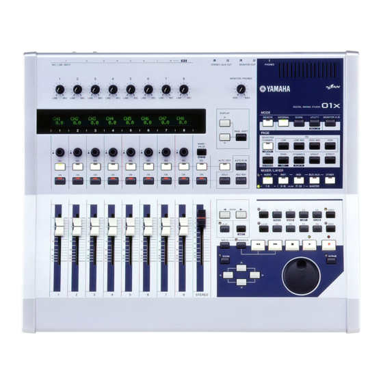
Page 8: Panel Layout
PANEL LAYOUT Top Panel mLAN MUSIC PRODUCTION STUDIO Copyright(c) Yamaha q Gain knobs w Display e Channel knobs r [SEL] buttons t [ON] buttons y Channel faders u [STEREO] fader i [NAME/VALUE] button o [MONITOR/PHONES] knob !0 [DISPLAY B/N] buttons... - Page 9 !6 [REMOTE] button !7 [INTERNAL] button !8 [SCENE] button !9 [UTILITY] button @0 [MONITOR A/B] button @1 [SELECTED CHANNEL] button @2 [EQ] buttons @3 [PAN] button @4 [SEND] button @5 [DYNAMICS] button @6 [GROUP] button @7 [EFFECT] button @8 [MIXER/LAYER] buttons @9 [BANK Q/W] buttons #0 [FLIP] button #1 [SHIFT] button...
- Page 10 #7 [E] button #7 E #8 [R] button #8 R #9 [A] button #9 A $0 [W] button $0 W $1 [S] button $1 S $2 [MARKER] buttons $3 [ZOOM] button $4 Cursor [ / /B/N] buttons $5 Dial $6 [SCRUB] button...
- Page 11 Rear Panel q MIC/LINE INPUT [MIC/LINE INPUT (XLR) 1/2] jacks [MIC/LINE INPUT (TRS phone) 3 ~ 8 (BAL)] jacks [MIC/LINE INPUT 8 (HI-Z)] jack w [STEREO/AUX OUT] jacks e [MONITOR OUT] jacks r [PHONES] jack t [mLAN 1/2] connectors y [ACTIVE] lamp u [PHANTOM +48V] switch i [DIGITAL STEREO IN/OUT] jacks o [FOOT SWITCH 1/2] jacks...
-
Page 12: Circuit Board Layout
CIRCUIT BOARD LAYOUT < Step 1> Rear view MLN2 Bottom view MLN2 < Step 2> Rear view Bottom view... -
Page 13: Disassembly Procedure
DISASSEMBLY PROCEDURE Side Panel (L, R) (Time required : About 1 min.) Remove the four (4) screws marked [140]. The side panel R can then be removed. (Fig. 1) The side panel L can then be removed in the same manner. - Page 14 2-4. Remove the eight (8) screws marked [112C] from the bottom cover. The bottom cover can then be removed. (Fig. 1) When installing the bottom cover, tighten the "1, 2 and 3" screws of those marked [112B] of the rear panel first. DM Circuit Board, MLN2 Circuit Board (Time required : About 3 min.) 3-1.
- Page 15 Escutchen & Contact (MLN2 Cicuit Board) Installation of Escutchen Place the Escutchen from the above and fit its claw into the hole in the MLN2 circuit board. (Fig. 2-1) Make sure that the Escutchen is horizontal to the circuit board and there is no clearance between the Excutchen and the MLN2 circuit board.
- Page 16 Fix the contact to the circuit board with 2 screws marked [60]. (Fig. 2-4) Fix the contact with manual soldering at 2 points. (Fig. 2-4) Use special care so that the contact is fixed securely. [60] [60]: Bind Head Tapping Screw-P 2.0 x 6 MFZN2BL (VG893800) (Fig.
- Page 17 [62] [62] [62] Rear view [63] Bottom view Knob spacers AN support angle Contacts Contacts [52A] AN support angle [52A]: Bind Head Tapping Screw-B 3.0 x 6 MFZN2Y (EP600130) [62]: Bonding Head Tapping Screw-B 3.0 x 10 MFZN2BL (VQ049800) [63]: Bind Head Tapping Screw-S 3.0 x 6 MFZN2BL (EP630210)
- Page 18 MF Support (A, B) 5-5. 5-5-1. Remove the eighteen (18) screws marked [1]. (Fig. 4-1) 5-5-2. As shown in Fig. 4-2, remove the MF supports (A, B) from the MF circuit board by sliding the supports toward outside of the circuit board. Don't bend the hooks of the MF supports (A, B) to prevent distortion.
- Page 19 PN1 Circuit Board (Time required : About 4 min.) 6-1. Pull out the dial knob from the control panel. (Fig. 1) 6-2. Remove the side panel L and R. (See procedure 1) 6-3. Remove the bottom cover. (See procedure 2) 6-4.
- Page 20 RE Circuit Board (Time required : About 6 min.) 8-1. Pull out the eight (8) encoder knobs from the control panel. (Fig. 1) 8-2. Remove the side panel L and R. (See procedure 1) 8-3. Remove the bottom cover. (See procedure 2) 8-4.
-
Page 21: Lsi Pin Description
LSI PIN DESCRIPTION CS5351-KSR (X3782A00) ADC (Analog to Digital Converter) ......21 CS8405A-CS (XZ349A00) DIT (Digital Audio Interface Transmitter) . - Page 22 HD6417709SF133 (X2081A00) CPU (SH3) DM: IC101 NAME FUNCTION NAME FUNCTION CKE/PTK5 CK enable / Port K Mode control RAS3L/PTJ0 RAS address bus / Port J Vcc(RTC) Power supply +1.8 V PTJ1 Port J XTAL2 CASL/PTJ2 CAS address bus / Port J Crystal oscillator EXTAL2 VssQ...
- Page 23 mLAN-NC1 (X2150A00) mLAN Node Controller 1 MLN2: IC008 NAME FUNCTION NAME FUNCTION Power terminal MCKO Master clock output for digital audio output WCKOD Delay output of WCKO TEST5 Test terminal TEST4 Test terminal IEC958O IEC60958 signal output from built-in DIT TEST3 Test terminal INT R SEL...
- Page 24 NAME FUNCTION NAME FUNCTION 135 IRQ# mLAN I/O In 8415 mode, interrupt request output from 205 P00/SRXD1 I/O General purpose port 00/serial I/F PH1 block to microprocessor 206 P01/STXD1 I/O General purpose port 01/serial I/F CE8# TRI MPU CE8 signal 207 P02/SCLK1# I/O General purpose port 02/serial I/F 137 CPU D0 I/O...
- Page 25 YTS440B-F (X3009B00) mLAN-PH2 (mLAN Packet Handler 2) MLN2: IC007 NAME FUNCTION NAME FUNCTION IRERRN Isochronous packet error flag input (Low active) BCK128O Bit clock output for digital audio output (128Fs) IRCVN Isochronous reception enable input (Low active) MCKO Master clock output for digital audio output (64Fs to 384Fs) IRXN Isochronous reception data enable input (Low active) Ground...
- Page 26 XCR3064XL-10 (X3628D00) CPLD (Complex Programmable Logic Device) MLN2: IC014 NAME FUNCTION NAME FUNCTION (Unconnected) I/O309 Output terminal which is write enable (L active) for the flash (Unconnected) memory assigned to CE9 zone of mLAN-NC1 Power supply (3.3V) (Unconnected) I/O209/TDI Terminal for loading data (Unconnected) (Unconnected) Power supply (+3.3V)
- Page 27 YSS910-S (XV988A00) DSP6 (Digital Signal Processor) DM: IC202 NAME FUNCTION NAME FUNCTION Power supply (3.3 V) Ground Ground DB13 System master clock input (60 MHz or 30 MHz) DB14 System master clock output (High or 30 MHz) DB15 Vdd5 Power supply (5 V) DB16 /SYNCI Sync.
- Page 28 YSS919B-H (XZ693B00) DSP7 (Digital Signal Processor) DM: IC210 NAME FUNCTION NAME FUNCTION PLLEN PLL enable input (0: PLL unuse, 1: PLL use) SIO32 /TEST Test mode setting (0: TEST, 1: Normal) SIO33 AVss Analog ground SIO34 SIO35 PLL filter Serial data bus AVdd Power supply (2.5 V) SIO36...
- Page 29 S1L51252F32S000 (X3775A00) PLLP2 (Gate Array) DM: IC602 NAME FUNCTION NAME FUNCTION (NC) (Connected to VSS on P.C.B.) (NC) (Pulled up on P.C.B.) (NC) (Pulled up on P.C.B.) Power supply Output port B8 (NC) (Connected to VSS on P.C.B.) Output port B9 (NC) (Connected to VSS on P.C.B.) IO power supply (3.3V)
- Page 30 SGH603064F-62F (XV973A00) REC2 (Gate Array) DM: IC402 NAME FUNCTION NAME FUNCTION Data bus Encoder input Ground Data bus Ground Ground Encoder input Data bus Ground Ground Data bus Ground Encoder input Not used Ground RA10 Encoder input RB10 RA11 RB11 Encoder input Address bus RA12...
- Page 31 LR38791 (XY631A00) CI-SUB (Gate Array) DM: IC403 NAME FUNCTION NAME FUNCTION FB17 Fader control LED8 LED control Ground Ground Power supply Power supply ...
- Page 32 CS8420 (XW559A00) SRC (Sample Rate Converter) DM: IC702 NAME FUNCTION NAME FUNCTION SDA/CDOUT Serial control data I/O (I C) / data out (SPI) TCBL Transmit channel status block start AD0//CS Address bit 0 (I C) / Control port chip select (SPI) OSCLK Serial audio output port bit clock input or output /EMPH...
-
Page 33: Ic Block Diagram
IC BLOCK DIAGRAM TC74VHC04FEL (XM332A00) HD74LS06FPEL (XH610A00) TC74VHC14FT (XV890A00) TC74VHCT04AF (XT777A00) Hex Inverter Hex Inverter Hex Inverter MF: IC101, 102 DM: IC102, 303 DM: IC118 AN: IC308 HD74LVC244ATELL (X2308A00) SN74AHC244PWR (X3262A00) TC74VHC157FT (X0199A00) TC74HC21AF (XJ622A00) TC74VHC244FT (XW234A00) Quad 2 to 1 Multiplexer Dual 4 Input AND Octal 3-State Bus Buffer DM: IC301, 306... - Page 34 SN74LVCC4245APWR (X3096A00) TC7WH00FU (TE12L) (XW946A00) TC7SH04FU (XS775A00) 74LVX4245MTCX (X3097A00) Dual 2 Input NAND Gate TC7S04F (XM182A00) Dual Supply Octal Bus Transceiver Inverter Gate DM: IC609 DM: IC203, 204 DM: IC119 MLN2: IC041 VCCA VCCB VCCB IN A OUT Y TC7WU04F (XN567A00) TC7SH08FU (XR680A00) TC7WH14FU (XY806A00) TC7WH04FU (XY363A00)
- Page 35 TA7291S (XF557A00) NJM4580ED (XT157A00) Motor Driver NJM4556AD (XQ824A00) Dual Operational Amplifier MF: IC103-106, 108-112 AN: IC101, 102, 107-109, Vref IC201, 202, 207-209, IC303-305, 307 AN: IC306 OUT1 +DC Voltage Output A Supply Inverting Output B Input A Non-Inverting Inverting Heat OUT2 OUT1 OUT2...
-
Page 36: Table Of Contents
CIRCUIT BOARDS AN (X3416C0) ........... 36/38 PN1 (X3414B0) ............44 DM (X3412D0) ..........40/42 PN2 (X3414B0) ............45 MF (X4778A0) ........... 46/47 RE (X4779B0) ........... 48/49 MLN2 (X3290C0) ..........50/51 Note : See parts list for details of circuit board conponent parts. AN Circuit Board MIC/LINE INPUT LINE/MIC... - Page 37 STEREO OUT MONITOR OUT PHONES HI-Z LINE/MIC LINE/MIC MONITOR/ PHONES Component side 2NA-WA21730-1...
- Page 38 AN Circuit Board 2NA-WA21730-2...
- Page 39 Pattern side 2NA-WA21730-2...
- Page 40 DM Circuit Board to AN-CN101 2NA-WA21700-1...
- Page 41 to LCD to MF-CN105 to MF-CN106 to PN1-CN101 to PN1-CN102 Component side 2NA-WA21700-1...
- Page 42 DM Circuit Board 2NA-WA21700-2...
- Page 43 Pattern side 2NA-WA21700-2...
- Page 44 PN1 Circuit Board to PN2-CN201 to PN2-CN202 to PN2-CN203 BANK UNDO EDIT SHIFT FLIP SAVE LOOP MARKER WRITE ZOOM SCRUB Dial to DM-CN404 to DM-CN405 Component side 2NA-WA21740...
- Page 45 PN2 Circuit Board REMOTE INTERNAL SCENE UTILITY MONITOR A/B DISPLAY PAGE SHIFT SELECTED CHANNEL LOW MID HIGH-MID HIGH AUTO EDIT SEND DYNAMICS GROUP EFFECT AUTO R/W REC RDY AUDIO INST MIDI BUS/AUX SOLO OTHER to PN1-CN103 to PN1-CN104 to PN1-CN105 Component side 2NA-WA21740...
- Page 46 MF Circuit Board STEREO Component side to DM-CN501 to DM-CN403 to DM-CN402 2NA-WB95270...
- Page 47 MF Circuit Board Pattern side 2NA-WB95270...
- Page 48 RE Circuit Board SEL4 SEL1 SEL2 SEL3 to DM-CN401 NAME/ VALUE SEL8 SEL6 SEL7 SEL STEREO SEL5 ON STEREO to PN2-CN204 Component side 2NA-WC02570...
- Page 49 RE Circuit Board Pattern side 2NA-WC02570...
- Page 50 MLN2 Circuit Board ACTIVE IEE1394 (S400) Component side 2NA-WA97910...
- Page 51 MLN2 Circuit Board Pattern side 2NA-WA97910...
-
Page 52: Updating Firmware
MIDI cable the factory defaults. Make sure you are not overwriting any (The YAMAHA USB-MIDI driver must be installed in the PC. important data. You should backup any important data to Also, the setting of the USB-MIDI driver should be your computer beforehand by using Studio Manager. - Page 53 Check that the port of Track 1 is USB 0-1 and reproduce SMF by Tempo 120. If the port is not USB 0-1, click on the port section to set it to USB 0-1. If USB 0-1 is not among selective items, check if connections are made properly and re-start XG works.
- Page 54 UX96 ////O1X OS Update //// Select Update Port MIDI-B/mLAN-5 ////O1X OS Update //// Waiting for OS Data..(MIDI-B) SELECTED REMOTE STANDBY/ON CHANNEL UTILITY SCENE KNOB-4 KNOB-7...
- Page 55 ////O1X OS Update //// Receiving OS Data (xxx%) ////O1X OS Update //// Writing OS into flash ROM.|----+----| Do you want to initialize backup data? YES NO Initializing backup data,please keep power on...
- Page 56 INSPECTIONS 1. Preparations 1.3 Initialization After upgrading the version of the program or installing a 1.1 Conditions new ROM, the values of the backup ROM must be initialized. (1) Set switches and VR knobs as follows unless otherwise specified. CAUTION 1) PHANTOM SW: OFF When you restore the factory default settings, all the settings 2) INPUT GAIN VR: LINE...
- Page 57 Pressing the encoder switch [KNOB-8] corresponding to 2.1. 21 MUTE NO will start operation without initialization. 2.1. 22 FADER LEVEL In this case, the fader set value is also cleared. As a result, 2.1. 23 SWITCH (DM) when starting the next time, the following message appears. 2.1.
- Page 58 Noise level • LINE Gain (INPUT GAIN VR knob at LINE.) Output level -90dBV or less Input 1kHz +4 dBu -10dBV ± 3dB Maximum output Output level Input 1kHz +18dBu Maximum output Output distortion 1% or less Input 1kHz +18dBu •...
- Page 59 2.2 Regular mode Selecting mLAN In the default state, mLAN AUTO W.CLK is disabled. 2.2.1 PHANTOM DC After pressing the encoder switch [KNOB-1] corresponding to Measurement condition Power ON ENABLE, press the encoder switch [KNOB-8] corresponding (1) Short between No.2 and No.3 pins of the XLR connector to YES on the next screen, and mLAN is selected.
-
Page 60: Circuit Boards
2.2.5 EFFECT Check 48kHz 10nsec or less 96kHz 10nsec or less Check at analog INPU3 PHONES. Set the fader level of INPUT3 to "0" and STEREO to "max". 2.2.3 Click noise Using the output volume knob, adjust the sound volume Measurement condition Power ON/OFF to the proper level so that the sound is not distorted. - Page 61 Do you want initialize backup data? REMOTE SCENE STANDBY/ON UTILITY KNOB-7 KNOB-8...
- Page 62 ERROR : Fader control parameter crashed! Use deault setting Do you want initialize backup data?
-
Page 64: An (X3416C0)
UTILITY W.CLK SELECT xxxxx [XXX : XXXXkHz] 2/2 INTERNAL xEXT-D.IN xEXT-mLAN UTILITY MENU SELECT REMOTE PATCH W.CLK D.I/O OSC. MIDI PREF. MONI. UTILITY mLAN AUTO W.CLK [XXX : XXXXkHz] 1/2 ENABLE/DISABLE DISPLAY N UTILITY KNOB-1 KNOB-3 KNOB-7 KNOB-8... - Page 65 EFFECT1 PATCH BYPASS MIX TYPE[REVERB HALL 100% EFFECT1 LIBRARY TYPE[REVERB HALL ] * 01 [Reverb Hall RECALL/STORE/CLEAR EFFECT1 LIBRARY TYPE[REVERB HALL ] * 37 [Delay ->ER. ] RECALL SURE? NO/YES DISPLAY N UTILITY KNOB-1 KNOB-5 KNOB-8 EFFECT KNOB-3...
-
Page 66: Test Program
TEST PROGRAM List of Test Programs Test name Measurement condition, etc. CPU MEMORY OK/NG CPU <->SDRAM I/F check SWITCH OK/NG, visual check ON/OFF of each switch (including Foot SW) SWITCH(PN) OK/NG, visual check ON/OFF of each switch SWITCH(RE) OK/NG, visual check ON/OFF of each switch ENCODER OK/NG... - Page 67 (Do not select "WDM" or "WDM+ASIO".) IEEE1394 (mLAN) cable: 1 pc. Once installation is completed, "AutoConnector for Foot switch (FC4, FC5) 01X" is automatically activated. Then make settings on Coaxial cable (75Ω) the dialog box as follows. MIDI cable SampleRate: 48KHz...
- Page 68 <Start-up screen> terminated before the end, pressing the [KNOB-7] or [KNOB-8] brings back the menu screen. On this screen, the YAMAHA O1X DIGITAL MIXING STUDIO test result is displayed in the test item space, that is, "O": (C)2003 YAMAHA CORPORATION completed as OK, "X": terminated before the end, "...
- Page 69 Description of Check Items 4.1 FLASH ROM/SDRAM function check ..4.2 Switch input check ..(01) CPU MEMORY (02) SWITCH (1) Outline (1) Outline The writing and reading functions are checked on SDRAM and The key condition of all switches is read. FLASH ROM and the result is displayed on LCD.
- Page 70 Have the function name of the switch to be checked flashed on 4.3 Switch input check (PN circuit board) ..(03) SWITCH (PN) the LCD and press the applicable switch. If a judgment is made (1) Outline that a switch other than the applicable one is turned on or a The key condition of all switches on the PN circuit board is multiple number of switches are turned on simultaneously, "NG"...
- Page 71 (3) Execution method in the faulty state (5) Check point when judged as NG To terminate before the end due to an error, press the [KNOB- The devices that can be diagnosed by this check are as follows. 8]. The screen returns to the execution select screen and "X" is displayed in the check item space.
- Page 72 4.8 LED lighting check ..4.9 LED lighting check (PN circuit board) ..(08) LED (09) LED (PN) (1) Outline (1) Outline The LED on the panel is checked visually for proper lighting The LED on the panel is checked visually for proper lighting by making the segments light from the upper left to the lower by making the segments light from the upper left to the lower right one after another and then making them flash by area.
- Page 73 4.10 LED lighting check (RE circuit board) ..4.11 LCD display check ..(10) LED (RE) (11) LCD (1) Outline (1) Outline The LED on the panel is checked visually for proper lighting Have all the dots of the LCD screen turned on, off and then on by making the segments light from the upper left to the lower to check visually that there is no scratch on the screen, missing right one after another and then making all the LED segments...
- Page 74 (2) Execution method in the normal state 4.13 DSP7 function check ..(13) DSP7 When proper operation of all signal items is confirmed, the (1) Outline screen returns to the execution select screen and "O" is displayed The check items on each signal related to DSP7 and judgment in the check item space.
- Page 75 Next, set the word After executing the user data backup, turn on the power while clock source back to "EXT-mLAn" (external PC) again to pressing the [UTILITY] and [AUDIO] switches of the 01X check that synchronization is provided. once again.
- Page 76 14:mLAN Signal items to be checked ERROR:xxxxxxxxxxxxx EXIT 1: Audio signal loop-back 2: Word clock frequency (48KHz) and lock 3: Word clock control, synchronization detection (4) Item description and error message 4: Connection of MLAN M/S-IN and MLAN M/S-OUT 1: Loop-back check using audio IN/OUT terminal SIO of terminals the audio signal loop-back ->...
-
Page 77: Dm (X3412D0)
(3) Execution method in the faulty state 2: LOCK Error If ERROR appears on the display, press [KNOB-8], and Error message: ERROR: LOCK checking comes to an end. The screen returns to the execution The lock detect function of the word clock fails to work select screen and "X"... - Page 78 (4) Item description and error message 4.19 AD14 to DA14 through function check ..(19) AD14DA14 (96k) None (1) Outline The input signal of AD1-4 is output to DA1-4 and the circuit of (5) Check point when judged as NG the analog signal system is checked.
- Page 79 21:MUTE MIC/LINE INPUT6 ->DM circuit board ->DIGITAL STEREO ANA MUTE OUT R The word clock of this unit is Internal 96KHz. When OK is selected, the following message appears on the (2) Execution method in the normal state LCD. After confirming the Mute Off state, press [KNOB-8]. When proper operation is confirmed, press [KNOB-8].
- Page 80 After setting faders 1 to 8 to "7.5" position and the STEREO 4.23 Switch input check (DM check) ..(23) SWITCH (DM) fader to "20", press the [KNOB-8], and that position is saved in (1) Outline the memory of the main unit. Then, the nine faders move down Have the function name of the switch to be checked displayed to approximately the lowermost position.
- Page 81 displayed on the LCD. The page can be changed among "FADER ERROR message: ERROR: NOT EXECUTE (22) AGING (COUNT), FADER AGING (MOVE MEASURE) and FADER LEVEL FADER AGING (FADER RANK) by pressing the [DISPLAY As the FADER LEVEL adjustment has not been DOWN/UP] button.
- Page 82 (5) Check point when judged as NG To terminate the operation, press [KNOB-8]. None (3) Execution method in the faulty state None 4.26 mLAN PATCH connection ..(32) mLAN PATCH (4) Item description and error message (1) Outline None The DSP patch required for the MLN2 circuit board operation check work is provided.
- Page 85 YAMAHA O1X DIGITAL MIXING STUDIO (C)2003 YAMAHA CORPORATION O1X (C) 2003 YAMAHA CORPORATION BOOT OS:V#.### BUILT DATE: 2003/**/** FIRM OS:V#.### ##### O1X DIAGNOSTICS PROGRAM ##### ______________----- 01:CPU MEMORY RECALL ##### O1X DIAGNOSTICS PROGRAM ##### ______________----- 02:SWITCH RECALL AUDIO UTILITY STANDBY/ON...
- Page 86 02:SWITCH PUSH ->xxxxxxxxx 01:CPU MEMORY ERROR:xxxxxxxxxx EXIT...
- Page 87 03:SWITCH (PN) PUSH ->xxxxxxxxx 05:ENCODER KNOB-1 ->Rxx EXIT 04:SWITCH(RE) PUSH ->xxxxxxxxx...
- Page 88 07:ENCODER KNOB-1 ->Rxx EXIT 06:ENCODER(PN) JOG ->0 EXIT...
- Page 89 08:LED 09:LED (PN) 08:LED 09:LED (PN)
- Page 90 10:LED (RE) 11:LCD 10:LED (RE) 12:DSP6 DSP6 TEST NOW...
- Page 91 13:DSP7 DSP7 TEST NOW... 12:DSP6 ERROR:xxxxxxxxxxxxx EXIT 13:DSP7 ERROR:xxxxxxxxxxxxx EXIT...
- Page 92 14:mLAN mLAN TEST NOW...
- Page 93 14:mLAN ERROR:xxxxxxxxxxxxx EXIT 14:mLAN AUTO TEST OK (CHECK MIDI-A,B &SET FS 96K) 14:mLAN mLAN TEST NOW...
- Page 94 15:W.CLOCK ERROR:xxxxxx EXIT 16:DIGITAL I/O RELEASE CABLE ENTER 16:DIGITAL I/O 17:AD14DA14 ERROR:xxxxxx EXIT...
- Page 95 19:AD14DA14 (96k) 18:AD58DA14...
- Page 96 21:MUTE CPU MUTE 21:MUTE ANA MUTE 21:MUTE MUTE OFF 20:AD58DA14 (96k) 22:FADER LEVEL SET UPPER LEVEL (+6/0dB) ENTER...
- Page 97 22:FADER LEVEL SET CENTER LEVEL (-7.5/-20dB) ENTER 22:FADER LEVEL SET LOWER LEVEL (-oodB) ENTER 22:FADER LEVEL FADER CALIBRATING ... 23:SWITCH (DM) PUSH=xxxxxxxxx ON 22:FADER LEVEL ERROR:xxxxxx EXIT...
- Page 98 30:FADER AGING ERROR:xxxxxx EXIT 30:FADER AGING (COUNT) COUNT=xxxxxxx EXIT 30:FADER AGING(MOVE MEASURE) RANGE=80 31:DSP PATCH AD14->DA14 AD12->DOUT INT48K EXIT 30:FADER AGING(FADER RANK) FADER SPEED = 28 30:FADER AGING ERROR:NOT EXECUTE (22)FADER LEVEL EXIT...
- Page 99 32:mLAN PATCH AD18->ML18 ML14->DA14 48KPLL EXIT 33:MIDI-B RELEASE CABLE ENTER 33:MIDI-B TEST OK EXIT 33:MIDI-B ERROR:xxxxxx EXIT...
-
Page 100: Trouble Diagnosis
TROUBLE DIAGNOSIS The trouble diagnosis is a function that enables to guess the trouble point when the unit does not appear to work even with the power turned on. For example, even when nothing appears on the LCD and even the TEST program cannot be accessed, the trouble point can be diagnosed by using this function. - Page 101 Bottom view LD101 (IC101) MLN2...
-
Page 102: Display Messages
Can’t save, erase, or edit the title because the song is read-only. mLAN MASTER NOW! This operation cannot be performed because the 01X is in mLAN Master mode. mLAN SLAVE NOW! This operation cannot be performed because the 01X is in mLAN Slave mode. - Page 104 • This may have no effect depending on the specifications of the As advanced as the 01X is, it too is susceptible to noise. Various connected device. types of noise may be generated and recorded to your audio...
-
Page 105: Midi Implementation Chart
MIDI IMPLEMENTATION CHART YAMAHA [DIGITAL MIXING STUDIO] Date : May/28,2003 Model:01X MIDI Implementation Chart Version : 1.0 Transmitted Recognized Remarks Function... Basic Default 1 - 16 1 - 16 Memorized Channel Changed 1 - 16 1 - 16 Memorized Default... -
Page 106: Midi Data Format
No relevant messages. The mLAN MIDI ports 1, 4 and 5 are used to communicate via MIDI with the 01X. The mLAN MIDI ports 2 and 3 are con- 3.3 System Real-time Messages nected directly to the MIDI-A and MIDI-B terminals of the 01X and do not communicate via MIDI with the 01X. -
Page 107: Parts List
PARTS LIST CONTENTS OVERALL ASSEMBLY ...............2 PN1 & PN2 CIRCUIT BOARD ASSEMBLY ...............4 RE CIRCUIT BOARD ASSEMBLY ......6 ELECTRICAL PARTS ............7 – 25 Notes : DESTINATION ABBREVIATIONS A : Australian model M : South African model B : British model O : Chinese model C : Canadian model Q : South-east Asia model... - Page 108 OVERALL ASSEMBLY • AC Adaptor (PA-300) This figure shows Japanese model. RE circuit board PN2 circuit board assembly: See page 6. assembly: See page 4. PN1 circuit board assembly: See page 4. 110a...
-
Page 109: Mf (X4778A0)
PART NO. DESCRIPTION REMARKS REF NO. RANK OVERALL ASSEMBLY (WA77440) WB461500 Control Panel WA969400 UMS-3144MD-7B Dust Proof Cushion (WB87380) EP600130 Bind Head Tapping Screw-B 3.0X6 MFZN2Y LCD Shield Plate (WB95690) EP600130 Bind Head Tapping Screw-B 3.0X6 MFZN2Y WA964900 PN1 Circuit Board Assembly EP600130 Bind Head Tapping Screw-B 3.0X6 MFZN2Y... - Page 110 PART NO. DESCRIPTION REMARKS REF NO. RANK V 8 4 6 6 0 0 0 AC Adaptor PA-300 AUS AAX34630 AC Cord V 9 9 7 3 6 0 0 AC Adaptor PA-300 K AAX51860 AC Cord WB122200 Cable IEEE1394 6P-6P2.0m CD-ROM CDROM 12cm Tools for O1X...
- Page 111 PN1 CIRCUIT BOARD ASSEMBLY PART NO. DESCRIPTION REMARKS REF NO. RANK WA964900 PN1 CIRCUIT BOARD ASSEMBLY (WA97830) Circuit Board PN (PN1+PN2) (WA21740) WA263600 Push Button Gray RTG1LGX2 Cursor(Left,Up,Down,Right BANK(Left,Right) V 2 6 4 6 5 0 0 Function Button Black SHIFT,EDIT,UNDO,LOOP,SAVE V 7 0 4 1 3 0 0 Function Button Dark Gray...
- Page 112 RE CIRCUIT BOARD ASSEMBLY PART NO. DESCRIPTION REMARKS REF NO. RANK WC365400 RE CIRCUIT BOARD ASSEMBLY (X4779B0) Circuit Board (WC02570) V 6 7 7 6 8 0 0 Push Button Dark Gray MR1G LENS ON(1-8,STEREO) V 8 6 0 0 1 0 0 Push Button White MR1LG LENS SEL(1-8,STEREO)
-
Page 113: Electrical Parts
ELECTRICAL PARTS PART NO. DESCRIPTION REMARKS REF NO. RANK ELECTRICAL PARTS WA217300 Circuit Board (X3416C0) WA217000 Circuit Board (X3412D0) WB952700 Circuit Board (X4778A0) WA979100 Circuit Board MLN2 (X3290C0) WA964900 PN1 Circuit Board Assembly (WA97830)(X3414B0) WA965000 PN2 Circuit Board Assembly (WA97830)(X3414B0) WC365400 RE Circuit Board Assembly (X4779B0) - Page 114 PART NO. DESCRIPTION REMARKS REF NO. RANK C0175 UU138220 Electrolytic Cap. 220.00 16.0V C0176 UU137470 Electrolytic Cap. 47.00 16.0V C0177 UU138220 Electrolytic Cap. 220.00 16.0V C0178 UU137470 Electrolytic Cap. 47.00 16.0V C0179 UR837470 Electrolytic Cap. 47.00 16.0V C0180 US145100 Ceramic Capacitor-F (chip) 0.1000 25V Z -0183 US145100...
- Page 115 PART NO. DESCRIPTION REMARKS REF NO. RANK * C0292 WC041200 Electrolytic Cap. 220.00 25.0V C0298 UU147470 Electrolytic Cap. 47.00 25.0V C0303 US145100 Ceramic Capacitor-F (chip) 0.1000 25V Z C0304 US145100 Ceramic Capacitor-F (chip) 0.1000 25V Z C0305 UU137470 Electrolytic Cap. 47.00 16.0V C0306 UU137470...
- Page 116 PART NO. DESCRIPTION REMARKS REF NO. RANK -109 XT157A00 NJM4580ED OP AMP * IC116 X3782A00 CS5351-KSR * IC117 X3782A00 CS5351-KSR IC201 XT157A00 NJM4580ED OP AMP IC202 XT157A00 NJM4580ED OP AMP IC207 XT157A00 NJM4580ED OP AMP -209 XT157A00 NJM4580ED OP AMP * IC216 X3782A00 CS5351-KSR...
- Page 117 PART NO. DESCRIPTION REMARKS REF NO. RANK R0142 RF357110 Carbon Resistor (chip) 11.0K D 1608 R0143 RF357100 Carbon Resistor (chip) 10.0K D 1608 R0144 RF357110 Carbon Resistor (chip) 11.0K D 1608 R0145 RD356100 Carbon Resistor (chip) 1.0K 63M J R0146 RF355330 Carbon Resistor (chip) 330.0 D 1608...
- Page 118 PART NO. DESCRIPTION REMARKS REF NO. RANK R0265 VC755500 Metal Oxide Film Resistor 4.7 2W J R0266 RD358100 Carbon Resistor (chip) 100.0K 63M J R0267 RD350000 Carbon Resistor (chip) 0 63M J R0268 RD353470 Carbon Resistor (chip) 4.7 63M J R0269 RD353470 Carbon Resistor (chip)
- Page 119 PART NO. DESCRIPTION REMARKS REF NO. RANK * VR202 WB216500 Rotary Variable Resistor C100.0K RK09D1130 MIC/LINE INPUT 6 * VR203 WB216500 Rotary Variable Resistor C100.0K RK09D1130 MIC/LINE INPUT 7 * VR204 WB216500 Rotary Variable Resistor C100.0K RK09D1130 MIC/LINE INPUT 8 VR301 V 2 3 4 5 6 0 0 Rotary Variable Resistor...
- Page 120 PART NO. DESCRIPTION REMARKS REF NO. RANK C0314 US145100 Ceramic Capacitor-F (chip) 0.1000 25V Z C0315 US145100 Ceramic Capacitor-F (chip) 0.1000 25V Z C0401 US145100 Ceramic Capacitor-F (chip) 0.1000 25V Z C0402 US035100 Ceramic Capacitor-B (chip) 0.1000 16V K -0413 US035100 Ceramic Capacitor-B (chip) 0.1000 16V K...
- Page 121 PART NO. DESCRIPTION REMARKS REF NO. RANK C0645 US044220 Ceramic Capacitor-B (chip) 0.0220 25V K C0646 VU195400 Electrolytic Cap. (chip) 10 16V C0647 US044220 Ceramic Capacitor-B (chip) 0.0220 25V K C0648 V 6 2 0 0 3 0 0 Capacitor 0.1000 16V M C0649 V 6 2 0 0 9 0 0...
- Page 122 PART NO. DESCRIPTION REMARKS REF NO. RANK IC301 X0199A00 TC74VHC157FT MULTIPLEXER IC303 XV890A00 TC74VHC14FT INVERTER IC304 VN686000 Photo Coupler PC410T IC305 VN686000 Photo Coupler PC410T IC306 X0199A00 TC74VHC157FT MULTIPLEXER * IC401 X2709A00 SN74AHCT245PWR TRANSCEIVER IC402 XV973A00 SGH603064F-62F GATE ARRAY (REC2) IC403 XY631A00 LR38791...
- Page 123 PART NO. DESCRIPTION REMARKS REF NO. RANK R0116 RD358100 Carbon Resistor (chip) 100.0K 63M J R0119 RD357100 Carbon Resistor (chip) 10.0K 63M J R0120 RD355100 Carbon Resistor (chip) 100.0 63M J -0122 RD355100 Carbon Resistor (chip) 100.0 63M J R0123 RD354680 Carbon Resistor (chip) 68.0 63M J...
- Page 124 PART NO. DESCRIPTION REMARKS REF NO. RANK R0608 RD356150 Carbon Resistor (chip) 1.5K 63M J R0609 RD356100 Carbon Resistor (chip) 1.0K 63M J R0615 RD350000 Carbon Resistor (chip) 0 63M J -0618 RD350000 Carbon Resistor (chip) 0 63M J R0620 RD350000 Carbon Resistor (chip) 0 63M J...
- Page 125 PART NO. DESCRIPTION REMARKS REF NO. RANK TR101 V 7 4 2 1 7 0 0 Transistor 2SC3324 GR,BL TE85 TR501 VV556400 Transistor 2SC2412K Q,R,S TR502 VS185600 Transistor 2SD1863 TV2 82-390 X0101 VS486900 Quartz Crystal Unit 8.0MHz SMD-49 * X0201 WA606100 Ceramic Resonator CSTLS30M0X53-A0...
- Page 126 PART NO. DESCRIPTION REMARKS REF NO. RANK R0124 RD255390 Carbon Resistor (chip) 390.0 0.1 J R0125 HV753220 Flame Proof C. Resistor 2.2 1/4 J R0126 RD255100 Carbon Resistor (chip) 100.0 0.1 J R0127 V I 1 9 6 0 0 0 Metal Film Resistor (chip) 3.0K 1/10 D R0128...
- Page 127 PART NO. DESCRIPTION REMARKS REF NO. RANK C0054 US062270 Ceramic Capacitor-SL(chip) 270P 50V J C0055 US064100 Ceramic Capacitor-B (chip) 0.0100 50V K C0056 US062270 Ceramic Capacitor-SL(chip) 270P 50V J * C0057 V 9 9 8 0 7 0 0 Monolithic Ceramic Cap. 22.000 6.3V K 3225 C0058 UB044100...
- Page 128 PART NO. DESCRIPTION REMARKS REF NO. RANK R0023 RD354330 Carbon Resistor (chip) 33.0 63M J R0024 RD356470 Carbon Resistor (chip) 4.7K 63M J R0026 RD350000 Carbon Resistor (chip) 0 63M J -0028 RD350000 Carbon Resistor (chip) 0 63M J R0029 RD357100 Carbon Resistor (chip) 10.0K 63M J...
- Page 129 PART NO. DESCRIPTION REMARKS REF NO. RANK WA964900 PN1 Circuit Board Assembly (WA97830)(X3414B0) WA965000 PN2 Circuit Board Assembly (WA97830)(X3414B0) Circuit Board PN (PN1+PN2) (WA21740) V 6 7 7 6 5 0 0 Push Button Black MR1B LENS EQ(LOW,LOW-MID,HIGH-MID, HIGH),PAN,SEND,DYNAMICS, GROUP,EFFECT V 6 7 7 6 8 0 0 Push Button Dark Gray MR1G LENS...
- Page 130 PART NO. DESCRIPTION REMARKS REF NO. RANK LD223 VU067800 LED Red SEL6210S-TP5 REC RDY LD224 VU067800 LED Red SEL6210S-TP5 SOLO LD225 VS704700 LED Red SEL2210W TP8 AUDIO,..OTHER Lamp LD226 V 6 3 0 8 7 0 0 LED Yellow SEL2710Y TP8 1-8,..MASTER Lamp R0102 HF454100...
- Page 131 PART NO. DESCRIPTION REMARKS REF NO. RANK -0227 VT332900 Diode 1SS355 TE-17 * EC201 WB272300 Rotary Encoder with SW XRE0122PVB25FINB1 Channel control 8 * EC202 WB272300 Rotary Encoder with SW XRE0122PVB25FINB1 Channel control 7 * EC203 WB272300 Rotary Encoder with SW XRE0122PVB25FINB1 Channel control 6 * EC204...
-
Page 132: Circuit Diagram
CIRCUIT DIAGRAM CONTENTS BLOCK DIAGRAM 3 – 5 OVERALL CONNECTOR CIRCUIT DIAGRAM OVERALL CIRCUIT DIAGRAM DM (001-007) ............... 7 – 13 AN (001-003) ............. 14 – 16 PN1 ..................17 PN2 ..................18 MLN2 (001-003) ............19 – 21 MF ..................22 RE .................. -
Page 133: Block Diagram
BLOCK DIAGRAM 001 +12A +16A +1.8D +3.3D AC Adaptor REGULATOR REGULATOR STANDBY/ON REGULATOR REGULATOR DC IN SW501 IC219 IC218 PA-300 AC IN IC505 IC503 JK501 +2.5D JK101 +48V REGULATOR REGULATOR MIC/LINE IC502 IC504 INPUT 1 CN501 JK102 PHANTOM +48V DC/DC +48V REGULATOR MIC/LINE... - Page 134 BLOCK DIAGRAM 002 MONITOR/ JK101 IC102A IC108A AK4382A IC303A PHONES IC305A JK301 AOUTL+ AD[1] 1ch/2ch DA[1] MIC/LINE AINR SDOUT SO 40 SDTI MONITOR LR MONITOR LR AOUTL- MONITOR OUT L INPUT 1 TR304 UNBAL (-10dBV) DSP7 IC301 VR103 (16P) (MIXER) +48V /RES-DAC IC303B...
- Page 135 BLOCK DIAGRAM 003 Xtal MLN2 Xtal mLAN2 I/F 20MHz 24.576MHz CN6 (100P) Packet-Master/Slave Up to 40MHz by Internal PLL Up to 393.216MHz by Internal PLL MIDI IN/OUT (5 port) 29, 30 110, 111 MIDI (UART) 42–45 PHY – LINK I/F MD8408B IEE1394 (S400) IC10 (64P)
- Page 136 OVERALL CONNECTOR CIRCUIT DIAGRAM DM–RE MFA18400 AC ADAPTOR CN202 CN401 JK501 AC IN DC IN (PA-300) CN201 PN–RE MFA18180 PN–PN WA619000 CN204 DM–LCD WB316800 PN–PN WA618300 CN201 CN202 CN203 CN101 PN–PN WA618300 CN103 CN104 CN105 DM–PN WB316900 CN101 CN404 DM–PN WB317000 CN102 CN405 AN POWER (WA53900)
- Page 137 DM CIRCUIT DIAGRAM 001 SYSTEM RESET to LCD INVERTER SDRAM FLASH ROM INVERTER TRANSCEIVER 28CC1-8825605-1 1 TRANSCEIVER DM CIRCUIT DIAGRAM 001...
- Page 138 DM CIRCUIT DIAGRAM 002 DRAM DRAM DSP7 DSP6 INVERTER D-FF TRANSCEIVER to MLN2-CN6 (P21) TRANSCEIVER D-FF to AN-CN101 (P14) 28CC1-8825605-2 2 DM CIRCUIT DIAGRAM 002...
- Page 139 DM CIRCUIT DIAGRAM 003 FOOT SWITCH 1 angle Photo Coupler INVERTER FOOT SWITCH 2 INVERTER MIDI A angle INVERTER Photo Coupler MIDI B MULTIPLEXER MULTIPLEXER Signal correspondence table of MIDISEL=0 Signal name (NG) Signal correspondence table of MIDISEL=1 Signal name 28CC1-8825605-3 1 DM CIRCUIT DIAGRAM 003...
- Page 140 DM CIRCUIT DIAGRAM 004 to MF-CN106 (P22) to MF-CN105 (P22) Transistor Array GATE ARRAY (CI-SUB) to RE-CN202 (P23) TRANSCEIVER GATE ARRAY (REC2) Transistor Array to PN1-CN102 (P17) D-FF to PN1-CN101 (P17) 28CC1-8825605-4 DM CIRCUIT DIAGRAM 004...
- Page 141 DM CIRCUIT DIAGRAM 005 µ PC2918T-E1(X2157A00) S3V20 (VR313500) REGULATOR +1.8V DIODE to AN-CN201 (P15) PHANTOM +48V ON OFF 1: INPUT 2: GND 3: OUTPUT 1: ANODE 4: GND 2: CATHODE to AN-CN202 µ PC2925T-E1(X0637A00) RK46 ( V8107700 ) (P15) DIODE REGULATOR +2.5V STANDBY/ON 1: INPUT...
- Page 142 DM CIRCUIT DIAGRAM 006 TRANSCEIVER NAND REGULATOR LP2980AIM5X-4.5 (X0527A00) REGULATOR +5V INVERTER INVERTER RESET 1: VIN 2: GND 3: ON/OFF 4: ADJ 5: VOUT DIR2 GATE ARRAY (PLLP2) INVERTER 28CC1-8825605-6 1 DM CIRCUIT DIAGRAM 006...
- Page 143 DM CIRCUIT DIAGRAM 007 BUFFER INVERTER DIGITAL STEREO DIGITAL STEREO 28CC1-8825605-7 1 DM CIRCUIT DIAGRAM 007...
- Page 144 AN CIRCUIT DIAGRAM 001 OP AMP OP AMP MIC/LINE INPUT 1 MIC/LINE INPUT 1 to DM-CN201 (P8) OP AMP OP AMP MIC/LINE INPUT 2 MIC/LINE INPUT 2 OP AMP OP AMP MIC/LINE INPUT 3 MIC/LINE INPUT 3 28CC1-8825607-1 2 OP AMP MIC/LINE INPUT 4 MIC/LINE...
- Page 145 AN CIRCUIT DIAGRAM 002 OP AMP OP AMP MIC/LINE INPUT 5 MIC/LINE INPUT 5 OP AMP OP AMP MIC/LINE INPUT 6 MIC/LINE INPUT 6 NJM78M05DL1A(XS534A00) REGULATOR +5V OP AMP OP AMP MIC/LINE INPUT 7 1: INPUT MIC/LINE 2: GND INPUT 7 3: OUTPUT NJM78M12DL1A(X2600A00) REGULATOR +12V...
- Page 146 AN CIRCUIT DIAGRAM 003 OP AMP OP AMP MUTE MONITOR/PHONES MONITOR OUT L UNBAL (-10dBV) OP AMP MUTE OP AMP MONITOR OUT R UNBAL (-10dBV) OP AMP MUTE OP AMP PHONES OP AMP MUTE OP AMP MUTE STEREO/AUX OUT L UNBAL (-10dBV) MUTE CONTROL MUTE...
- Page 147 PN1 CIRCUIT DIAGRAM Dial FLIP SCRUB SCRUB FLIP ZOOM to PN2-CN201 (P18) BANK WRITE ZOOM YELLOW LOOP BANK MARKER SAVE to DM-CN404 (P10) EDIT SHIFT SAVE EDIT to PN2-CN202 (P18) MARKER LOOP UNDO UNDO YELLOW to PN2-CN203 (P18) to DM-CN405 (P10) 28CC1-8825608-1 PN1 CIRCUIT DIAGRAM...
- Page 148 PN2 CIRCUIT DIAGRAM SELECTED SELECTED REMOTE LAYER AUDIO AUTO R/W AUDIO REMOTE CHANNEL CHANNEL ORANGE YELLOW SEND INST INTERNAL INST SEND INTERNAL AUTO EDIT to PN1-CN103 (P17) ORANGE YELLOW ORANGE DYNAMICS LOW-MID SCENE MIDI LOW-MID MIDI DYNAMICS SCENE REC RDY ORANGE YELLOW to RE-CN201 (P23)
- Page 149 MLN2 CIRCUIT DIAGRAM 001 µPC2933T-E1 (XS516A00) RB160L-40 (VS597600) DIODE REGULATOR +3.3V 1: V in 1: ANODE 2: GND 2: CATHODE 3: V out not installed mLAN-NC1 INVERTER IEE1394 (S400) RESET EEPROM not installed REGULATOR not installed +3.3V ACTIVE not installed not installed not installed not installed...
- Page 150 MLN2 CIRCUIT DIAGRAM 002 installed not installed not installed CPLD not installed installed CY7C024AV-25AC not installed not installed not installed not installed RESET INVERTER installed installed 28CC1-8827928-2 2 MLN2 CIRCUIT DIAGRAM 002...
- Page 151 MLN2 CIRCUIT DIAGRAM 003 TRANSCEIVER TRANSCEIVER installed TRANSCEIVER installed installed not installed installed installed TRANSCEIVER not installed not installed installed BUFFER BUFFER not installed INVERTER installed TRANSCEIVER installed not installed not installed installed installed installed installed installed to DM-CN202 (P8) 28CC1-8827928-3 1 not installed MLN2 CIRCUIT DIAGRAM 003...
- Page 152 MF CIRCUIT DIAGRAM to DM-CN501 (P11) MOTOR MOTOR MOTOR MOTOR MOTOR DRIVE DRIVE DRIVE DRIVE DRIVE to DM-CN402 (P10) MOTOR MOTOR MOTOR MOTOR DRIVE DRIVE DRIVE DRIVE to DM-CN403 (P10) STEREO MULTIPLEXER 28CC1-8825606-1 (Analog SW) MF CIRCUIT DIAGRAM...
- Page 153 RE CIRCUIT DIAGRAM SEL 1 SEL 2 SEL 1 SEL 2 SEL 3 SEL 4 SEL 3 SEL 4 SEL 5 SEL 6 SEL 5 SEL 6 NAME/ SEL 7 SEL 8 SEL 7 VALUE SEL 8 SEL STEREO ON STEREO STEREO STEREO to PN2-CN204 (P18)